Electronics Productions
The fourth week and almost a month! Time goes by so fast. This was one of the most stressful weeks so far
Assignments
- Group Assignment
- Characterize the design rules for your in-house PCB production process send a PCB out to a board house
- Individual Assignment
- Make and test a micro controller development board
- Personalize the board
Hero Shots
General Information
Note: This is my first time with electronic production, which is a very engaging and existing process. In this section, I will try to explain electronics on a surface level. Be certain and warned, that there could be mistakes in this section.
PCBs
A Printed Circuit Board (PCB) is a fundamental component in the world of electronics. It serves as a platform for connecting and supporting various electronic components to create functional circuits.
The structure of a PCB consist of two different layer types. A non-conductive substrate material provides mechanical support for the components and circuit traces and a conductive layer is laminated, laminated to the substrate material. The most basic version is a one-sided PCB, with one conductive layer on the top. Two-sided PCBs have a conductive layer on both sides, while multi-layered PCBs have additional layers inside (sandwich structures). In this weeks assignment only one-sided PCBs where used.
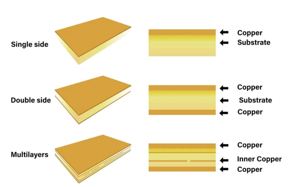
PCBs are classified by the material used for the conductive and base layer. The choice of PCB material is crucial in determining the performance, reliability, and cost of the final electronic device. Different materials offer various properties, and selecting the right one depends on factors such as the application, operating environment, and performance requirements. Here are some common PCB materials. FR-4 is the most widely used PCB material. It is a glass-reinforced epoxy laminate with flame-retardant properties. In general FR-4 boards have a good mechanical strength, excellent electrical insulation, and are cost-effective. However, FR4 isn't ideal for all situations, especially high-frequency designs. FR-1, FR-2, and FR-3 is typically used for single-layer PCBs in low-cost applications. Unlike FR-4, they have a paper substrate, that is less of a health risk when milling. However, they are not suitable for thermal postprocessing (e.g. for soldering paste). There are many other PCB material for special applications, such as flex PCB materials. In this week, only one-sided FR-4 was used as material.
Milling
In general, there are several options to create a PCB. Most commonly used are etching and milling. Milling is a process used to create custom circuit boards by removing unwanted copper from a blank board, leaving behind the desired circuit traces. This method is an alternative to traditional etching processes and is often used for prototyping or low-volume production. Additionally, it is less environmentally harmful, as no chemicals are involved in the process of milling.
For milling the basic need of equipment are a milling machine, end mills (bits), and fixturing. A CNC (Computer Numerical Control) milling machine is commonly used for PCB milling. It allows for precise control over the milling process. There are many variatioution of CNC milling machine, depending on the precision and the equipment they are very different in price also. In this weeks assignment we used two different milling machines.

When cutting a material it is important to fix the piece to the bed. Fixturing is a critical aspect of the PCB milling process, ensuring that the PCB material is securely held in place during milling to achieve accurate and precise results. Proper fixation helps prevent movement and vibrations, which can negatively impact the milling process. The typical approached of fixturing are double sided tape, clamp, and a vaccuum table. Additionally, it is important to put a sacrificial layer under the PCB material during milling in case of mistakes with the z-Axis leveling.
Generating a Fabrication Output
After designing a PCB, there are different possibilities to create a producible fabrication output.
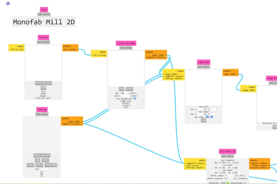
Mods
The Mods Project is giving the possibility to create a .rml file out of an .png file. The .rml file is like g-code and gives information about the movement of the axis. It is a accepted file format for the Roland CNC machines.
To start: right-click and choose "program" and choose "new program". Then select the shown output file.
This is the starting window for your program, that should occur.
Select the .png file from your computer.
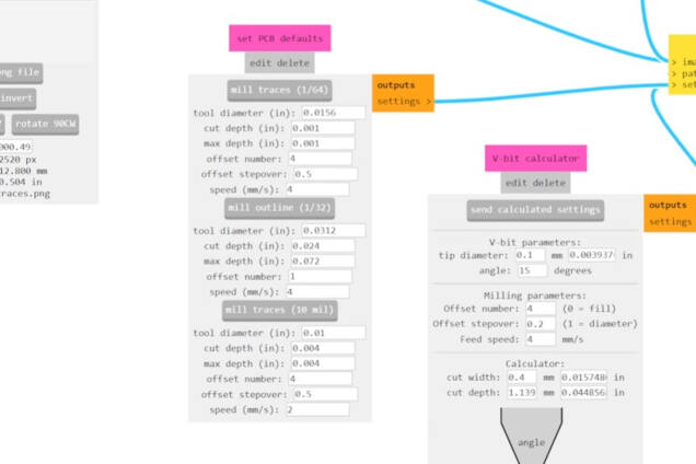
Enter your needed parameters, for the material and the cut (be aware of the units). Update the values to the other tabs by clicking on the grey buttons.
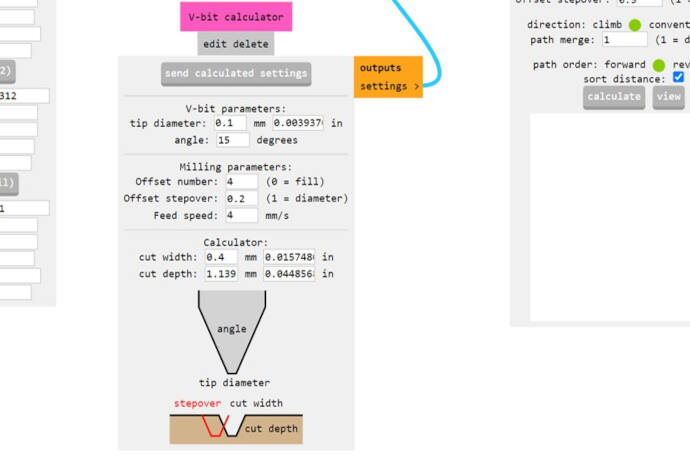
Enter your tool (bit) parameters and send the information to the other taps by pressing the grey button.
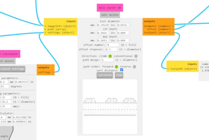
Click on "calculate" and then "view" to see the output.
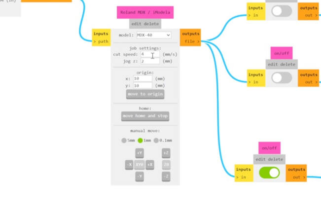
Enter the right machine (here Roland M-40) and change the origin if needed (here 1mm and 1mm).
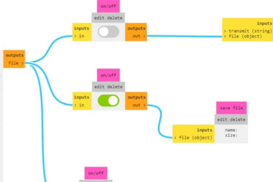
Enable the the "input/output" tap and click on "save file".
KiCAD
KiCadis an open-source electronic design software and has several possibilities of fabrication outputs. In this section you can find the explanation of generating a gerber file.
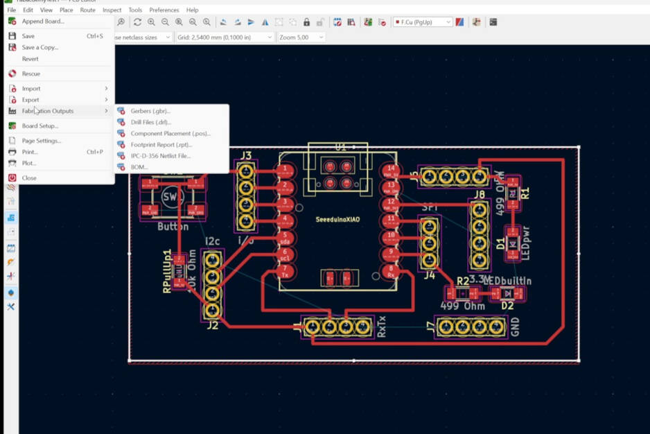
When you have finished your design, you go to "File", "Fabrication Output", and click on "gerber .grb"
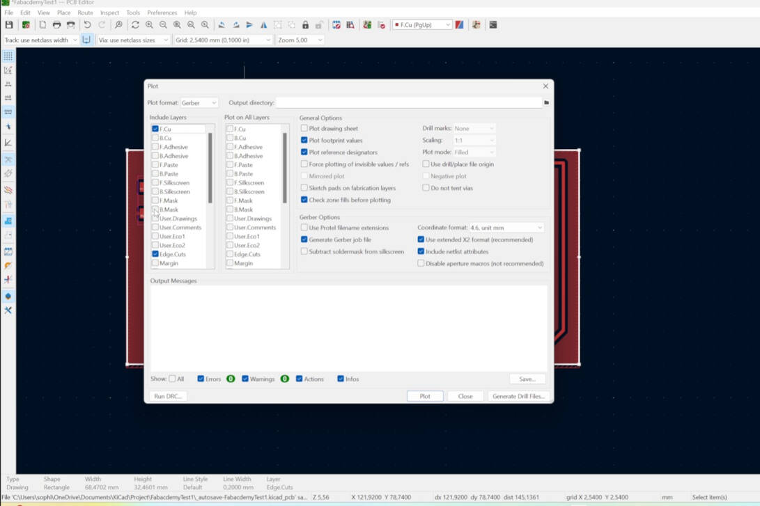
Select your layers. Here the F.Cu and EdgeCuts were needed.
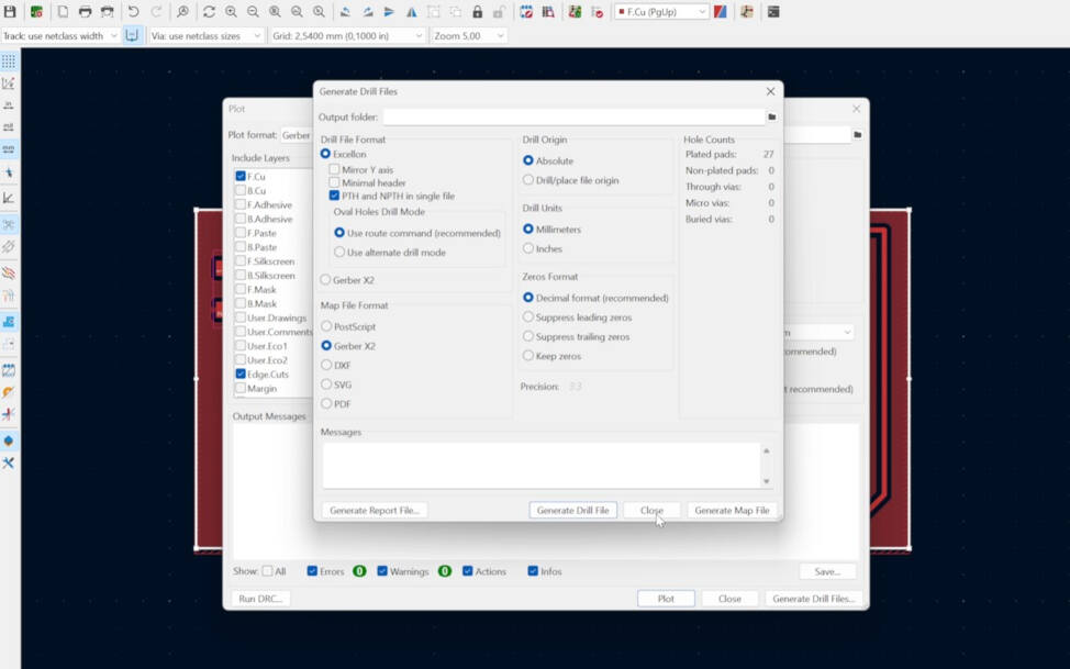
Click on "Generate Drill File". Select "PTH and NPTH in a single file" and be sure that the drill origin in "absolute" and the drill unit is "millimeter".
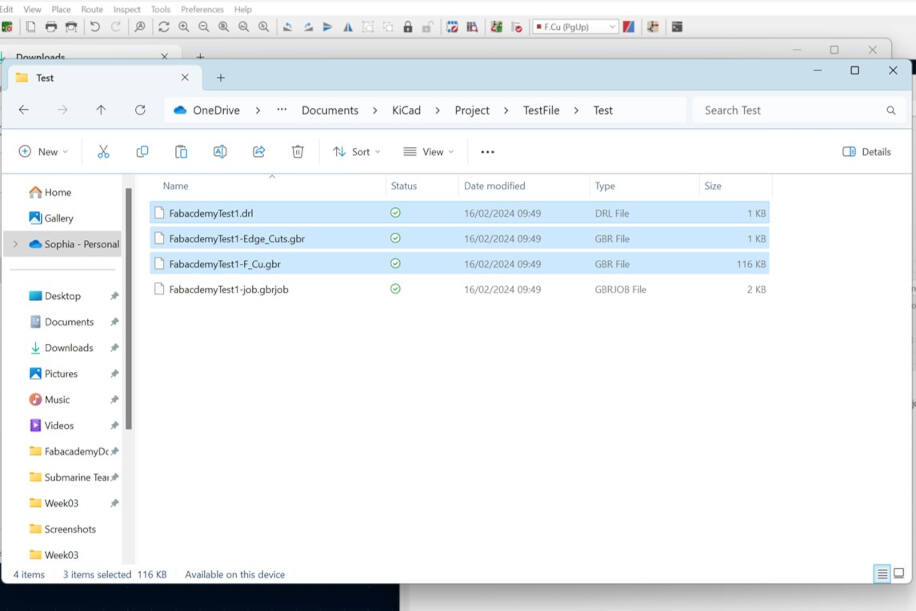
For the job on the LPKF the selected files are needed: two .grb file and one .drl file.
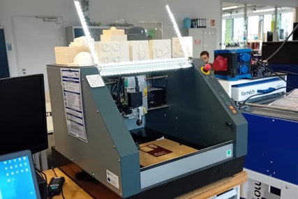
Milling Machine
In the lab in Kamp-Lintfort there are two operating small CNC milling machines for milling PCBs: Roland M-40 and the LPKF.
Roland M-40
Setup
The set up of the machine consists of the Roland M-40, the computer that is connect to it (used to control), and a vacuum cleaner for the milled material.
To initiate a milling operation, it is crucial to properly prepare the PCB material and secure it to the machine bed. The laboratory employs one-sided photosensitive FR-4 for PCBs, necessitating the removal of the photosensitive coating using acetone. To verify the absence of the photosensitive layer, observe a lack of shine on the material. Additionally, confirm that the material is of the correct size.
Prior to milling, inspect the cleanliness of both the machine bed and the interior of the Roland machine. Any debris between the bed and sacrificial layer or the sacrificial layer and the PCB material can result in surface irregularities and milling errors. It is essential to maintain a clean environment, as dust can compromise the adhesion of the double-sided tape used to affix the PCB material. Utilize a vacuum for cleaning the machine's interior thoroughly.
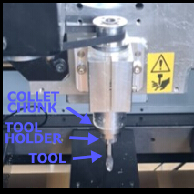
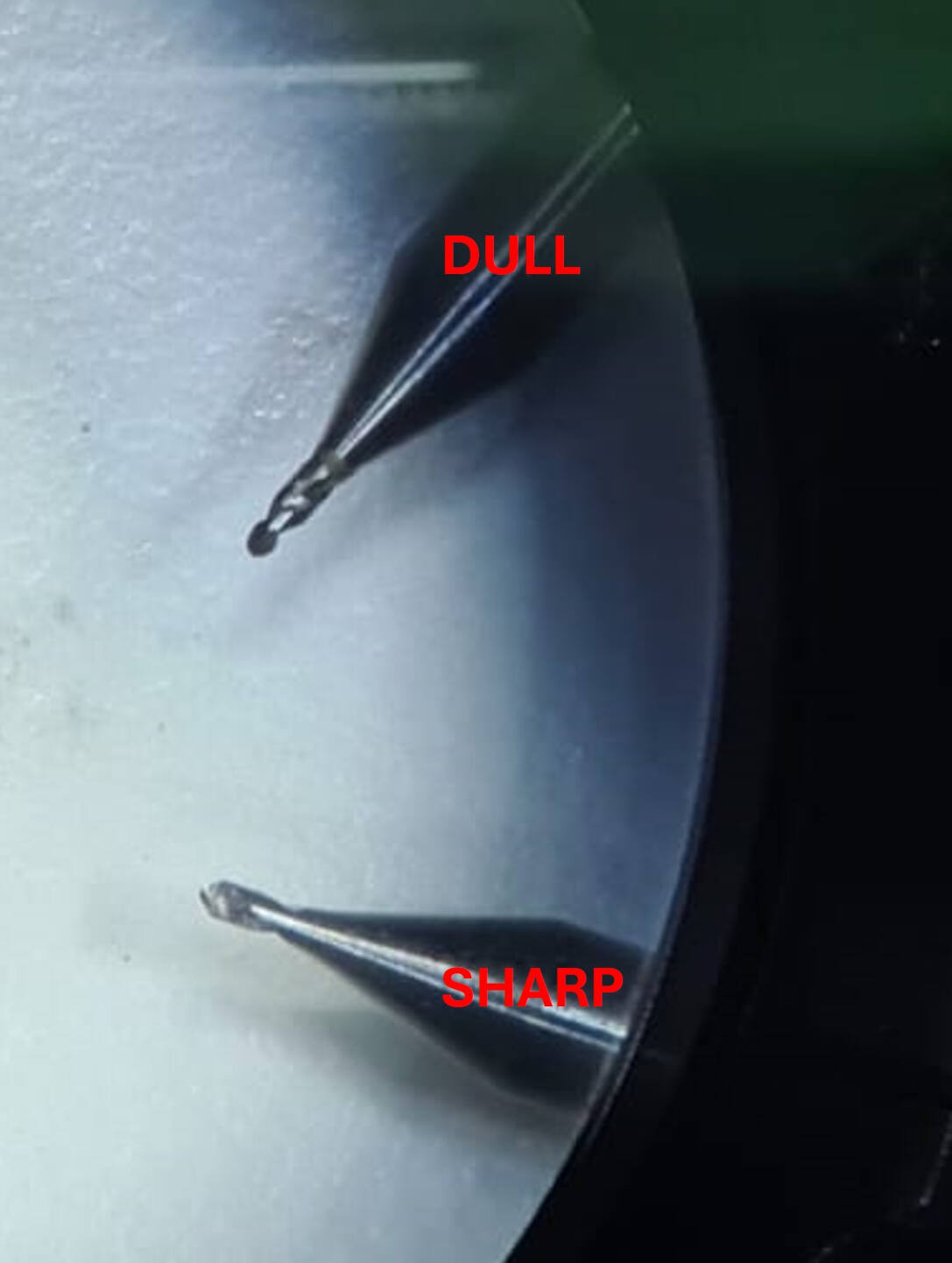
The subsequent step involves selecting the appropriate drill bit for the milling operation. Opt for a V-bit with a diameter of 0.4 mm and a 15° angle on the tip. When it comes to exchanging or inserting a drill bit, utilize two wrenches—one for the collet chuck and the other for the tool holder. Hold the collet chuck securely with one wrench while loosening the tool holder with the second wrench. Exercise caution to catch the tool once it is released.
IMPORTANT: DO NOT LET THE TOOL FALL DOWN! That can damage the bit severely, so it can not be used anymore.
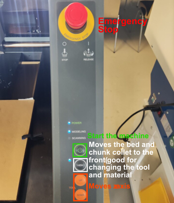
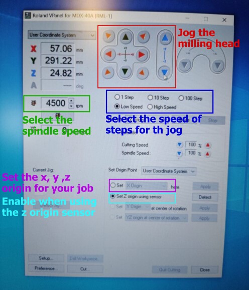
Controls
To Turn on the machine use the switch on the right side. Then use the start button on the panel. Open the Roland V-Panel on the computer. If the software shows an error of not being connected to the machine check if the Roland is turned on or if the USB connection is unplugged. For moving the CNC head use the speed options and the arrow buttons in the panel. NOTE: The control of the x-axis is the other way around as it moves the bed not the CNC head.
However, the job was promptly halted by our local instructor who observed that the tool was cutting too deep. The excessive dust production and machine sound indicated the issue. The mistake was traced back to an oversight in the material thickness setting, which was subsequently corrected to 1.5 mm before restarting the job.
For the second attempt, an alternative approach was adopted—loosening the tool until it made contact with the surface and then tightening it again. Despite implementing this method, the tool failed to touch the surface during the job, necessitating another interruption. The underlying cause appeared to be a slight upward movement of the tool during the tightening process.
To address this issue, we implemented the z-leveling sensor as a final solution. In this process, the sensor is strategically positioned between the tool and the material, and the 'Set Z origin using sensor' function is activated in the VPanel on the computer. This initiates an automatic leveling of the z-axis. Through this method, successful leveling was achieved, paving the way for the completion of the initial cut—referred to as the characterization process.
Characterization
As previously stated, we utilized a file supplied by the Fabacademy for the characterization process and generated a
fabrication output file using Mod. Additional details regarding the characterization process can be accessed on the
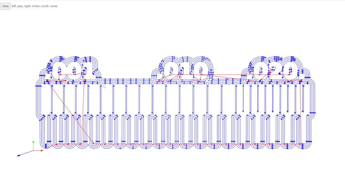
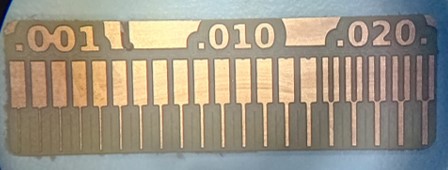
group assignment's page (see here). The completed characterization demonstrated impeccably clean edges, with no traces failing
to connect, even when dealing with very high-resolution traces (0.001). This outcome indicates a high level of tool precision,
a well-secured bed fixture, an undamaged tool, and accurate parameter settings.
LPKF
The second CNC machine for PCB milling in the lab, was the LPKF.
Setup
The Setup of the LPKF consists of the CNC machine itself, a computer to process files and send jobs to the machine and a dust extractor.
To commence a milling operation, proper preparation of the PCB material and secure fixation on the bed are crucial steps. Details regarding the preparation of the PCB material can be found in the preceding chapter. For fixturing, it's essential to note that the LPKF bed utilizes a vacuum system to secure the material in place and eliminate dust. Consequently, there is no need for double-sided tape; instead, using masking tape along three edges of the material proves sufficient. Ensure the absence of any dust or material particles between the sacrificial layer and the PCB material, as well as between the sacrificial layer and the bed.
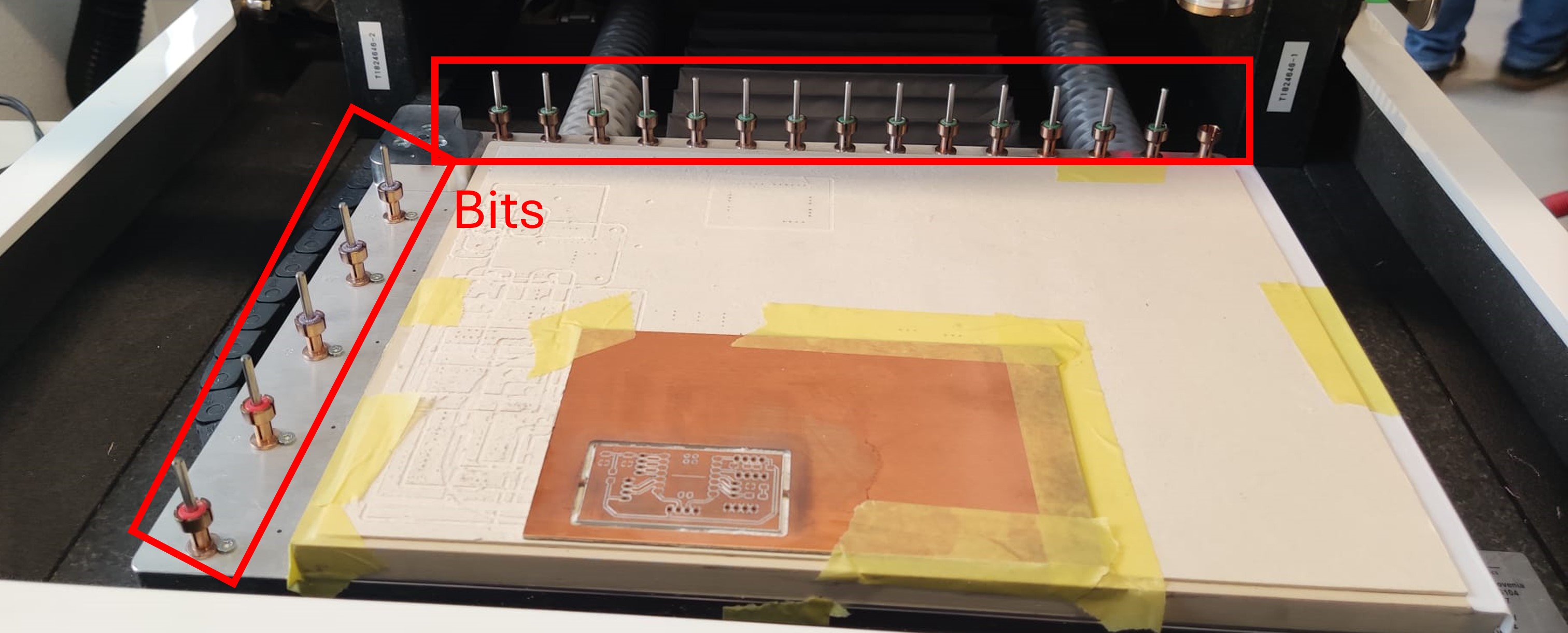
For both drill and milling bits, it's crucial to note that all bits are securely housed within the machine's enclosure, and the machine autonomously manages their use throughout the milling process. The software is designed to prompt users to replace drill bits at appropriate intervals, eliminating the need for manual checks on bit conditions. This automated system streamlines the operational efficiency and maintenance of the machine.
Controls
The machine is operated and job initiation is facilitated through the 'LPKF Circuit Pro PM' software provided by the company. To commence a job, follow the outlined steps below:
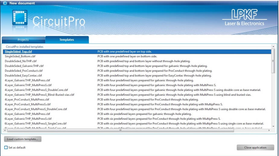
Open the software and click on "File" and click on "New Document". Go to "Template" and choose "Single-sided Top", click on "Close application".
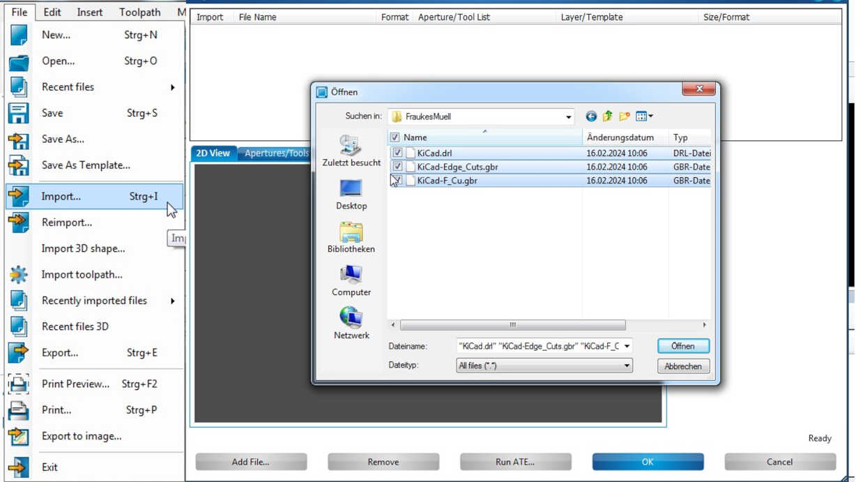
Go to "File" and click on "Import". Choose your folder and select all three file you exported from KiKad.
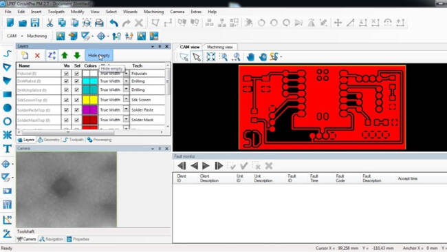
The main window will show the layers. Click on "Hide Empty" to see the layers relevant to your job.
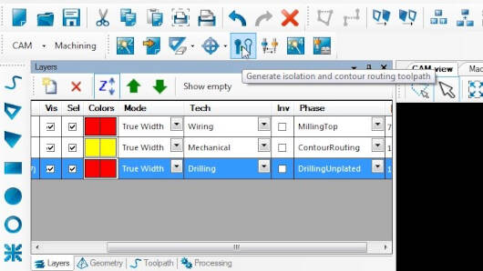
The drilling layer might be missing a "Tech" and "Phase" description. Choose "Drilling" for the "Tech" and "Drilling Unplugged" for the "Phase". After that click on "Isolation" (button highlighted in the picture).
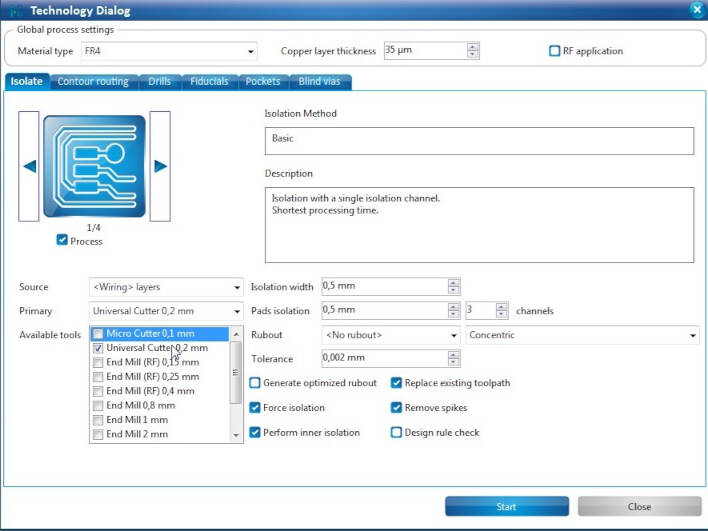
Choose "Universal Cutter 0.2 mm" as the primary tool, Turn off all the "available tools" except "Universal Cutter 0.2 mm". Choose "Isolation": 0.5, "Pad Isolation":0.5, and no rebound. Enter Copper layer thickness 35 microns.
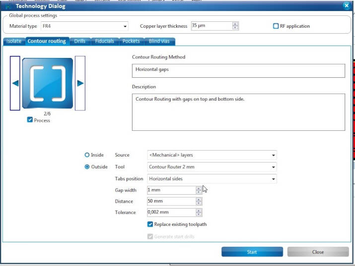
Go to tab "Counter routing" (source should be mechanical layer). Select either 3/6 or 2/6 as the counter routing. Clap width should be 1 mm, distance 50, and tolerance 0,002 mm.
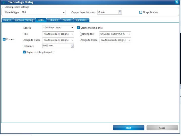
Navigate to the "Drills" tab with the source set to the mechanical layer. Choose "Create marking drills" and click on "Start". If warnings regarding pockets or fiducials appear, consider them normal. In the case of tool-related warnings, verify the tool positions in the holders adjacent to the bed. Occasionally, a tool may not be securely fixed in its holder and may require manual assistance.
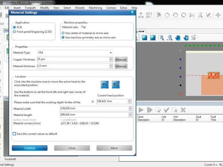
Click on the "Wizard" button, represented by a wand icon, and initiate the process by clicking "Start." A "Material" window will appear. Ensure that the "Copper Thickness" and "Material Thickness" are correctly set to the specified values (in our case, 35 microns and 1.5 mm). The next step involves setting the "Location." You can conveniently drag and drop the design to your preferred position. Additionally, utilize the tool holder as markers for precise positioning. Set points P1 and P2 (diagonal points) to verify that the machine's head aligns correctly for milling the PCB. After pressing continue, The "Placement" window occurs, where the PCB can be relocated, rotated, or even copied to create several of them. After that press continue.
After these steps, save your job on the computer, as the machine can recover a job very easily and use the saved file, if problem occur. The machine will start the milling.
Characterization
Soldering
For soldering we used the solder station in the lab in Kleve, not Kamp-Lintfort.
Setup
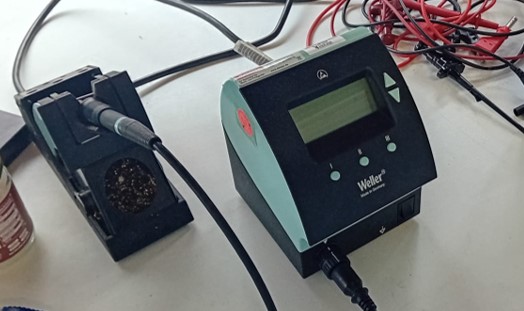
To facilitate soldering, a soldering station is required, comprising the soldering iron (equipped with a handle), the solder
stand base (featuring a soldering sponge for cleaning the iron), and the soldering main machine responsible for heating the iron.
The soldering machine offers three preset temperature values (1, 2, 3), and for more precise adjustments, temperature can be fine-tuned
using two arrow buttons located on the side.
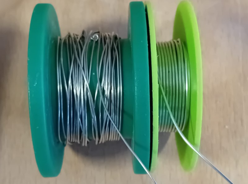
We utilized a Tin Copper alloy solder wire with a diameter of 1.0 mm, as well as a Tin Nickel alloy with the same diameter.
It's important to note that in Germany, the use of solder alloys containing lead is prohibited.
To enhance solder quality, the application of soldering flux is recommended.
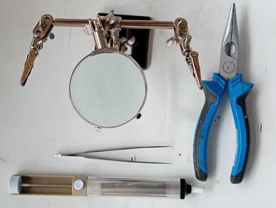
In addition, having a set of tweezers proves valuable for precisely placing small electrical components, while forceps are handy for cutting sections of solder wire from the spool. A stand with clips and a loupe can aid in stabilizing the PCB board during work. Additionally, a desoldering suction pump is useful for efficiently removing excess solder in case of mistakes or overuse.
IMPORTANT: Before you start turn on an air extraction! Do not inhale the fume of the solder.
Operation
To begin soldering, you have the flexibility to choose which component to place first. Start by applying a small amount of solder to one of the designated patches on the PCB where the component should be situated, and a small amount of flux on the joint of the component. Use tweezers for small components, heat the solder slightly to create a small molten pool.
IMPORTANT: SOME COMPONENTS CONDUCT ELECTRICITY ONLY IN ONE DIRECTION! use the multimeter to the right direction of the componentCarefully position the component onto the molten solder, allowing it to settle into place. If a misplacement occurs, it's easily rectifiable by reheating the solder, adjusting the component's position as needed. This method provides a controlled and adaptable approach, ensuring precise component placement and offering the convenience of corrections if required. Apply a small amount of soldering flux to the soldering joints.
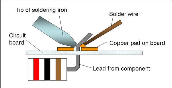
Touch the soldering iron to the joint, heating both the component lead and the PCB pad. Hold it in place for a few seconds. Introduce the solder wire to the joint, allowing it to melt and flow evenly over the connection. Ensure the solder wets both the component lead and the PCB pad. Withdraw the soldering iron, but keep the components steady to prevent any disturbance until the solder solidifies. Examine the solder joint for a shiny, smooth appearance. Wipe the soldering iron tip on a damp sponge or brass wire cleaner to remove excess solder. Allow the joint to cool before moving or testing. Repeat the process for each solder joint in your project.
Check-Up
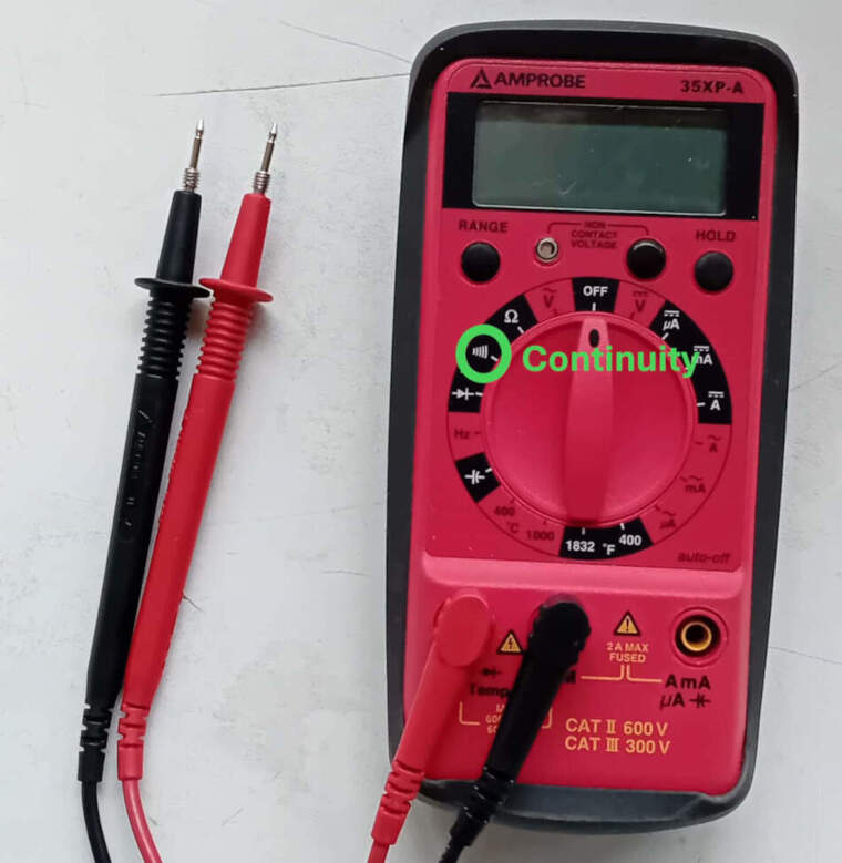
Using a multimeter can help you verify the success of your soldering connections. This can be done by checking the continuity. Turn on the multimeter and set it to the continuity or resistance mode. The continuity mode typically has a symbol that looks like a sound wave (∞) or a diode. Ensure the PCB or circuit you soldered is isolated from any power source. Identify the points on the PCB where you want to check continuity. These are typically the soldered joints or connections, the power traces and the ground, and adjacent connection or joints.
Place one probe on one end of the soldered connection and the other probe on the opposite end. If you are testing a component (like a resistor or diode), place the probes on either end of the component. If you're using the continuity mode, you should hear a beep or see a change in the display. This indicates that there is continuity, and the soldering connection is intact.
After verifying the connections, proceed to connect your PCB to an electrical source. If you notice excessive heat or any changes in color, promptly disconnect the power source. It is crucial to prioritize safety and prevent potential damage. For added assurance, incorporate LEDs into the PCB design that emit light when the PCB is plugged in. These LEDs can be integrated directly into the PCB layout or embedded within the microchip utilized for the PCB. This visual indicator serves as a real-time confirmation of the power supply status, enhancing both safety and diagnostic capabilities.
My first Board
After learning the theory in the lab and our local instructor showed us with an example board to work on the machines and soldering, we started to create our first own PCB.
Design
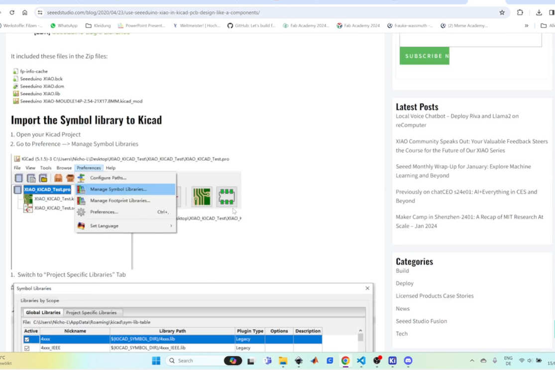
For the design we got a tutorial from our local instructor in KiKad. We started with getting a library for components for KiCad, that we use for Fabacademy.
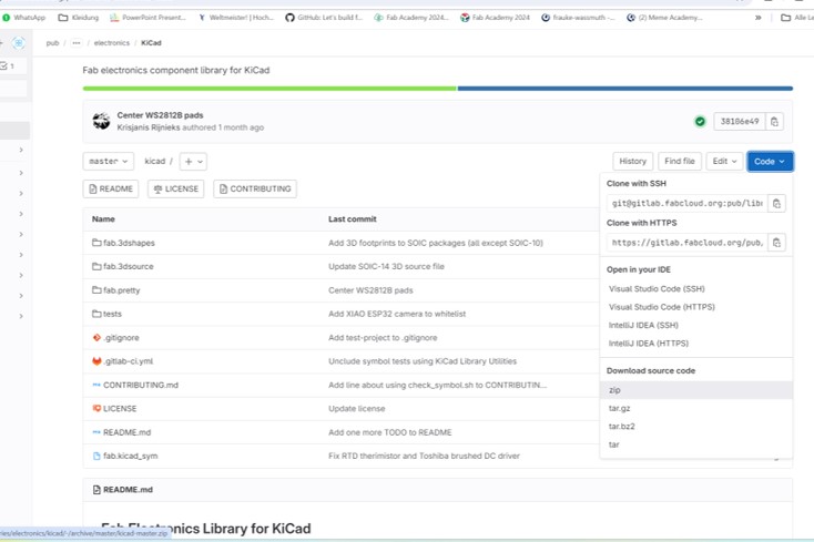
Before starting with KiCad, download this folder as a .zip file for a component library that is made for Fabacademy (download). Then extract the folder on your local computer.
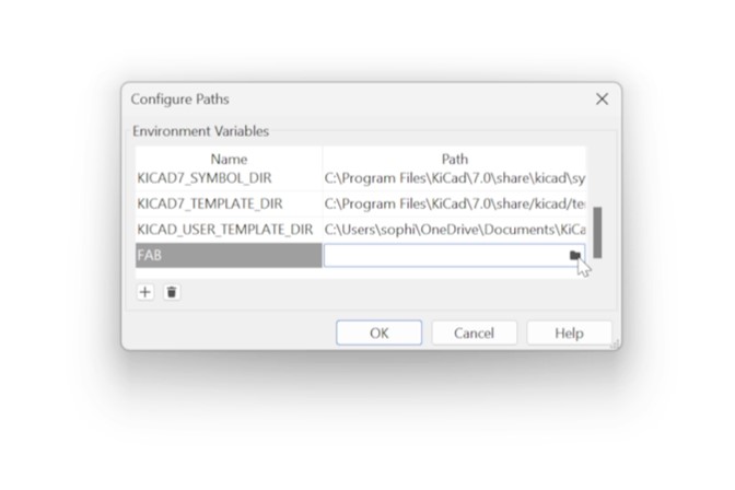
Open KiCad, select "Preferences", and click on "Configure Paths". Click on the "plus" button in the occurred window. Name the path you created as you prefer and then click on the "folder" button on the right to select the path of your extracted folder.
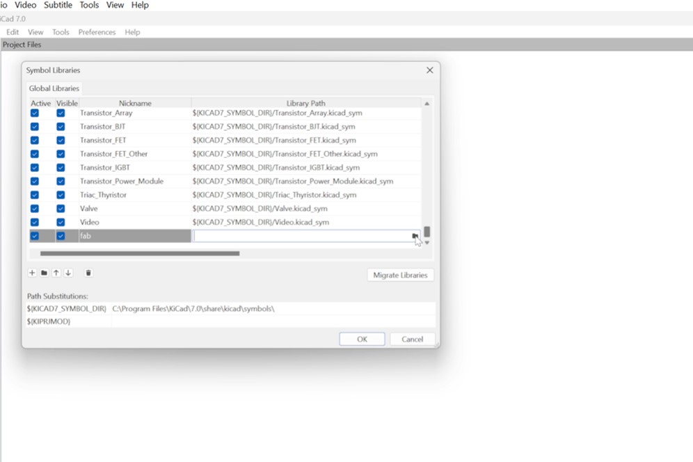
Select "Preferences", and click on "Symbol Libraries". Click on the "plus" button in the occurred window. Name the path you created as you prefer and then click on the "folder" button on the right. Select the .sym file in the folder.
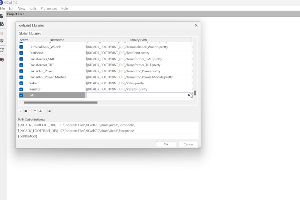
Select "Preferences", and click on "Manage Footprint Libraries". Click on the "plus" button in the occurred window. Name the path you created as you prefer and then click on the "folder" button on the right to select the path of the "pretty" folder.
We went on starting our first project.
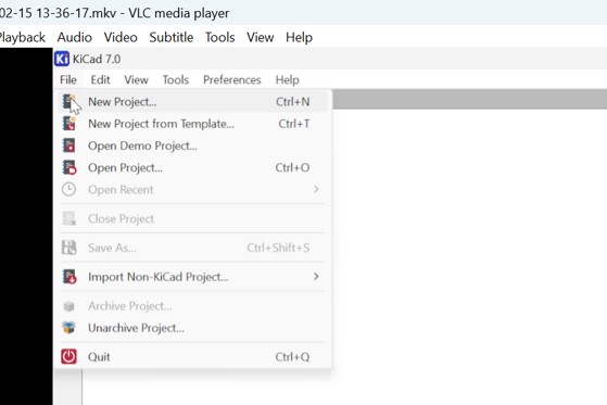
Select "File" and click on "New Project".
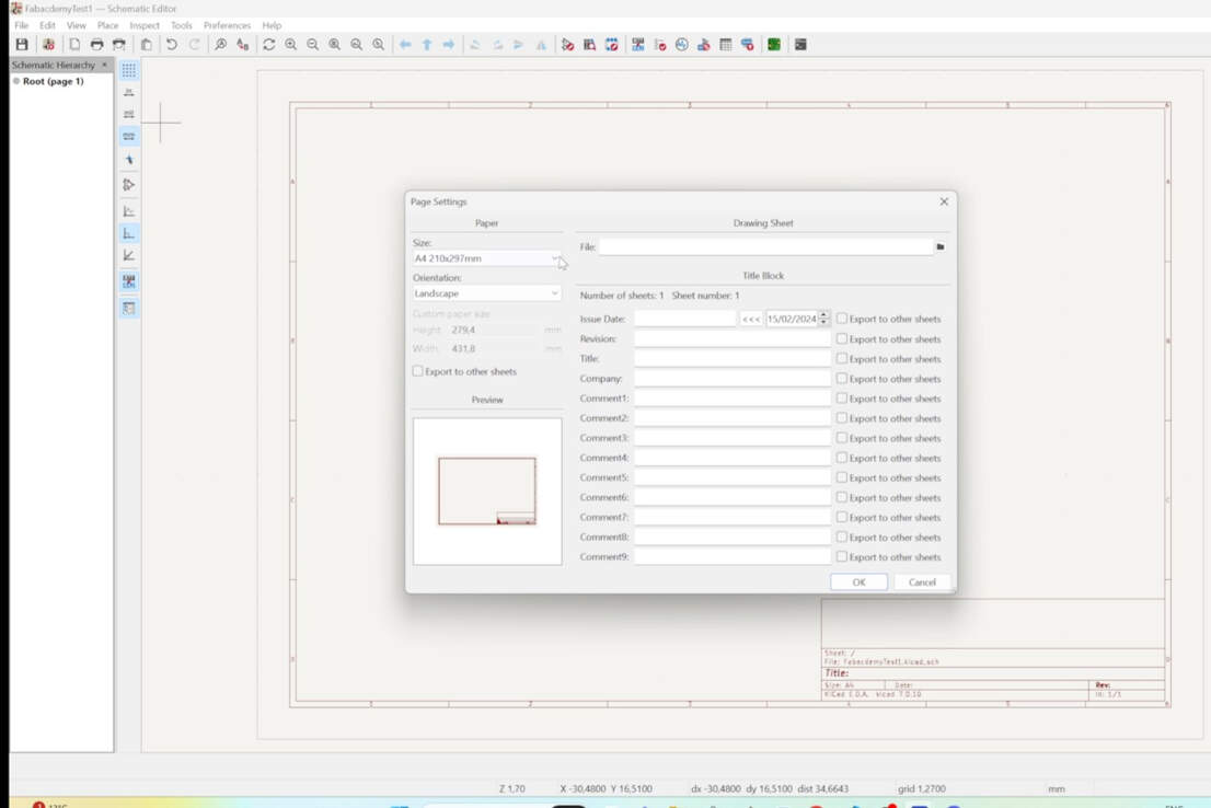
Two types of files should occur on the screen. Click on the "Schematic" file. select file and click on "Document Setting" and choose your settings.
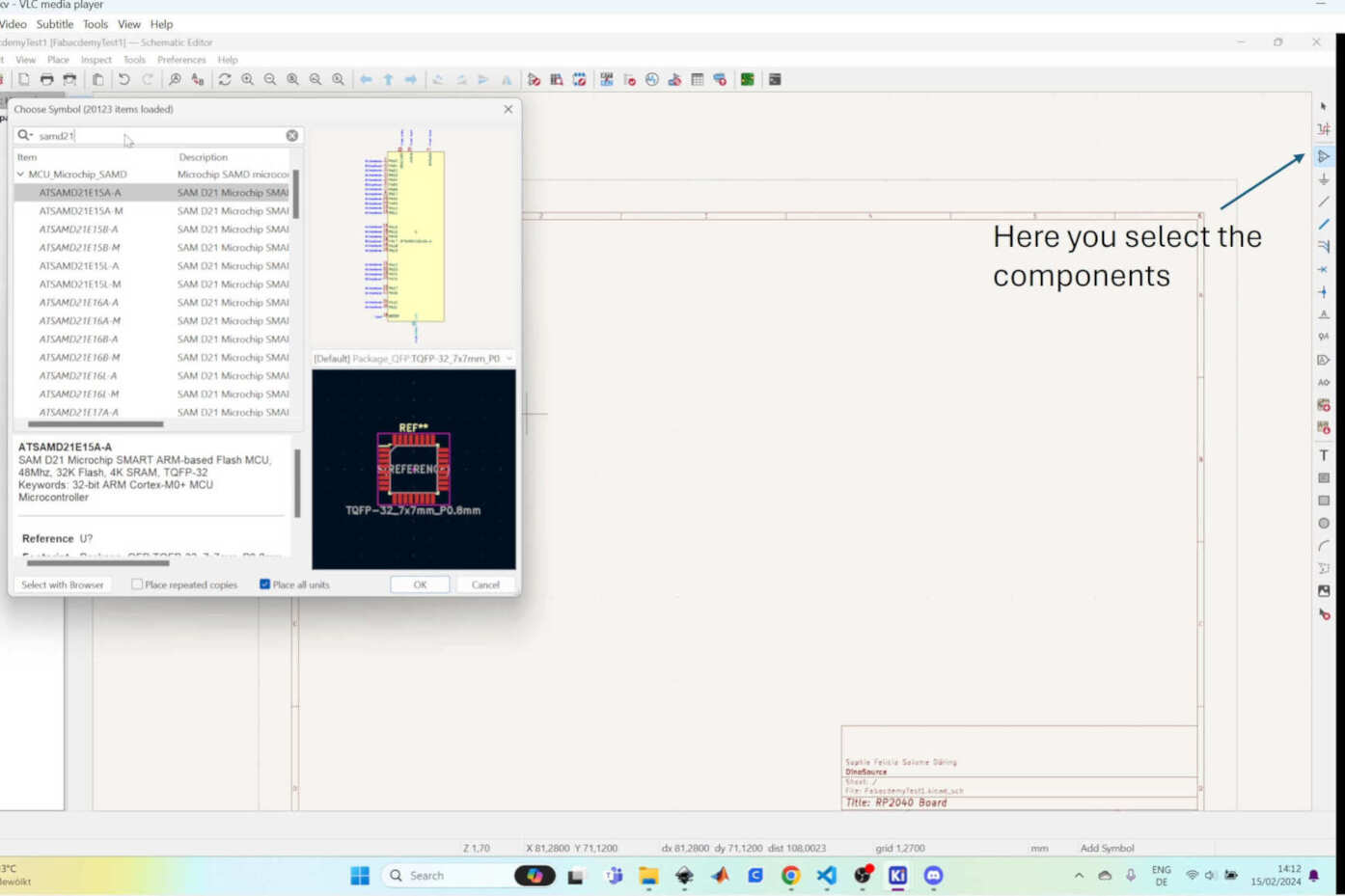
We then noticed when opening the components panel, to add components, that the SAMD-7021 we would use was missing in the library.
Therefore, our instructor send us a link with the folder and needed instruction for including the microcontroller.
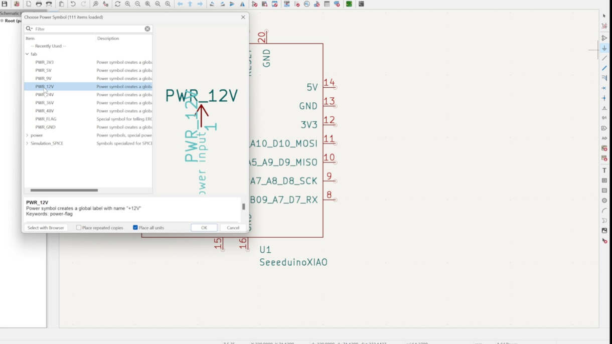
Now the microcontroller was added to the library. Therefore, we able to add it to the sheet and then continue with adding power symbols.
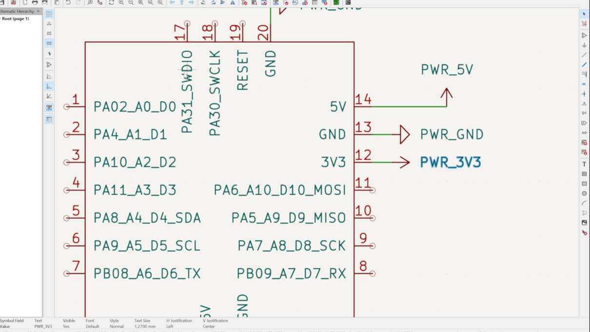
Every component and power symbol can be rotated (press R), the properties and description can be changed (press E), and can be connected to each other with wires (Add wires on the right side).
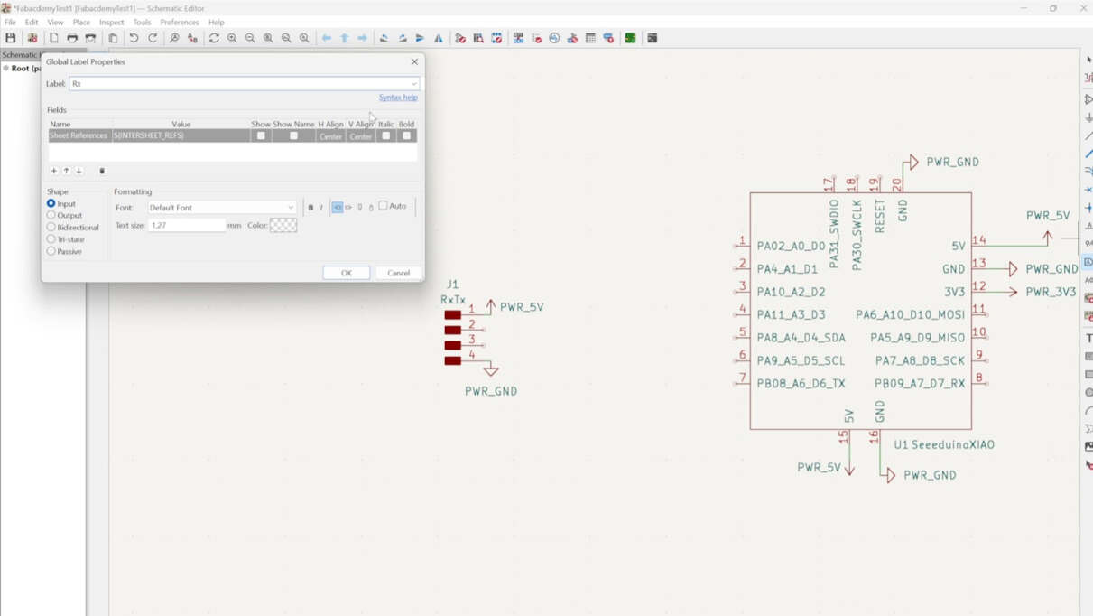
To illustrate the connections between components and the microcontroller, the label function was employed. This involves creating a label and linking it to two connections that are intended to be interconnected.
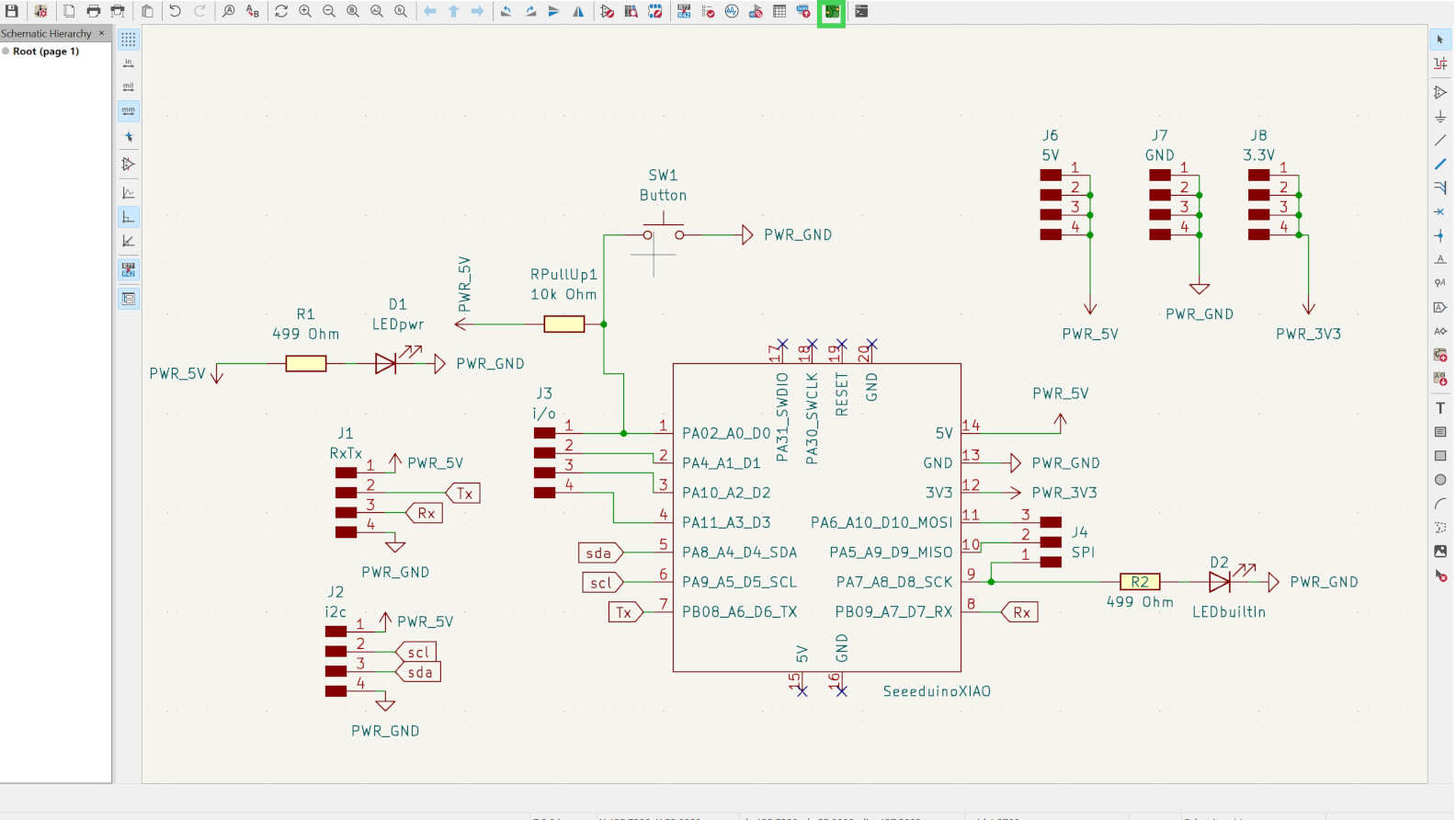
The finished schematic design, consited of a button, 6 4x1 pins, 1 3x1 pins, 3 resistors, 2 LEDs, and the microcontroller.
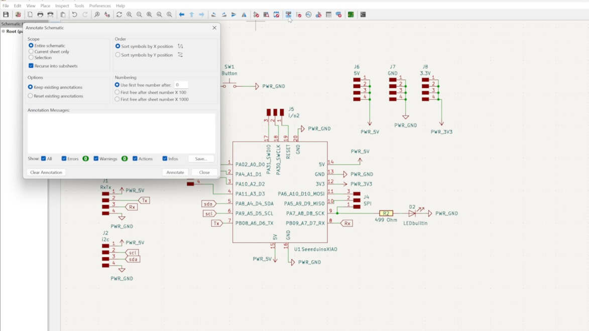
We then checked, if the annotation were correct (every components needs their own annotation, no doubles), and pressed annotate.
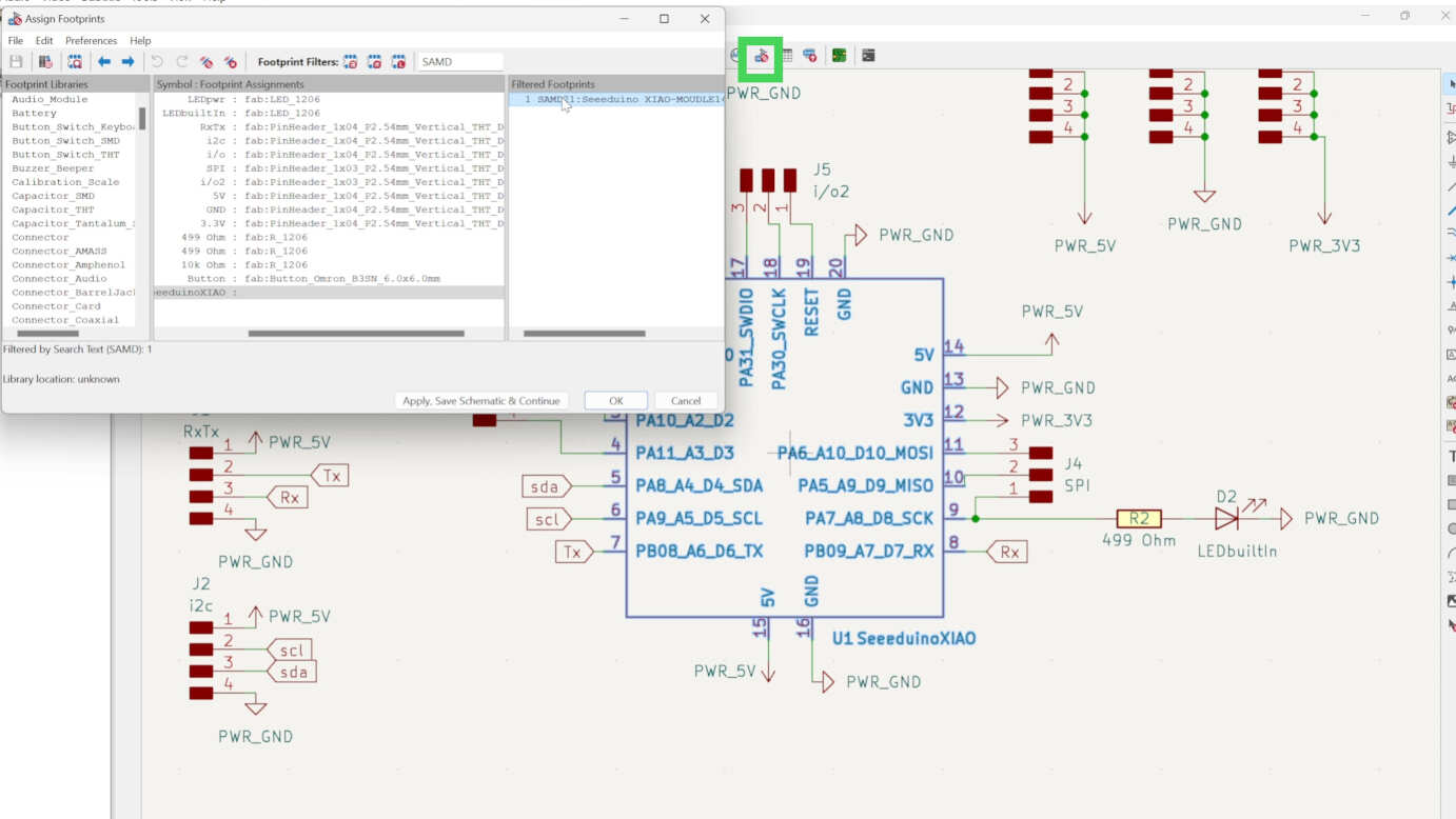
After that we took a look into the footprints, if they are all correct. As the Seeeduino did not have any, we searched in the searchbar of the window for SAMD7021 and enter the suggested footprint to the Seeduino.
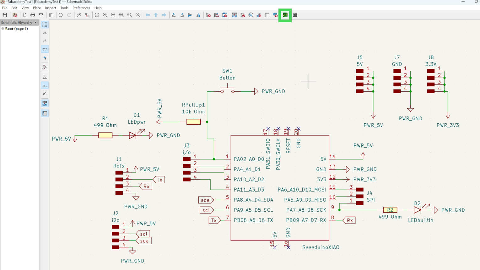
We then pressed on this button to open the PCB designer.
After that we took a look into the footprints, if they are all correct. As the Seeeduino did not have any, we searched in the searchbar of the window for SAMD21 and enter the suggested footprint to the Seeduino.
We then pressed on this button to open the PCB designer.
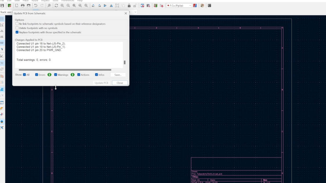
The PCB designer will then update your design. If you have a warning about measurement, it is a minor calculation error, because of inches and mm. You can ignore that warning.
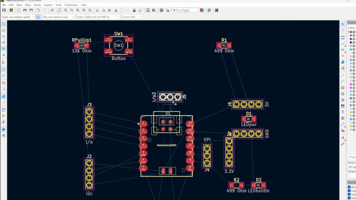
You can then move your pieces and arrange them. Press ctr if, you need fine adjustment, R for rotating, and align and group parts by click on to components and go to the right click menu. You can always change parts by going back to the schematic drawing. To update your PCB design press B.
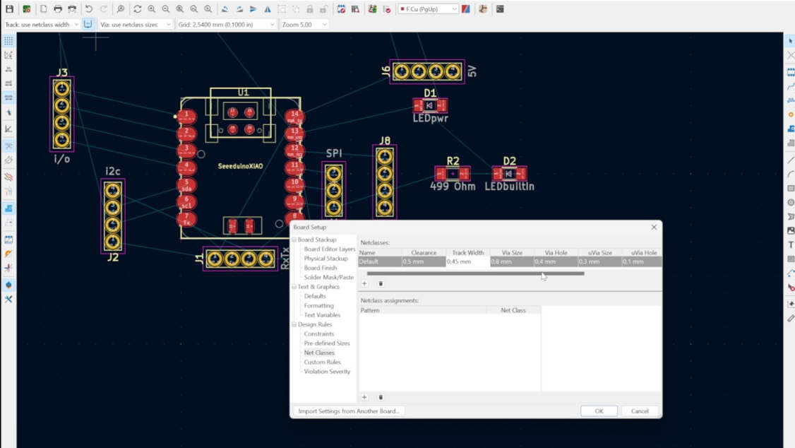
Go to "file" and click on "Board Setup". In the "Net Classes" menu you can choose the right track width and clearance (we used Clearance: 0.5 mm and Track width: 0.45 mm)
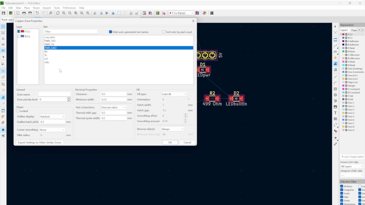
We then created a "Zone" and changed the values of it in a way, that everything that is not a trace should ground (values in the picture).
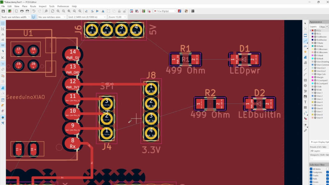
We then connected everything with "route tracks" (press X). It is important to not create island, where components are surrounded by traces and not connected to the ground.
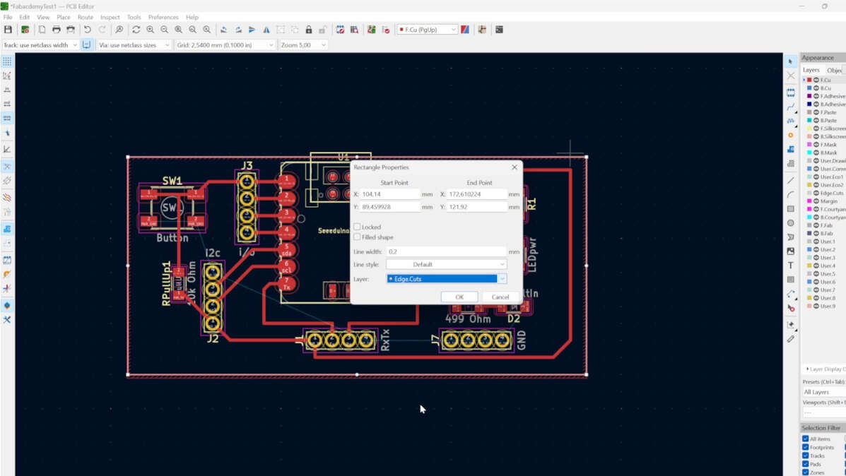
We then used the rectangle tool, surrounded the components and pressed E (Properties). We changed the layer to "Edge Cuts".
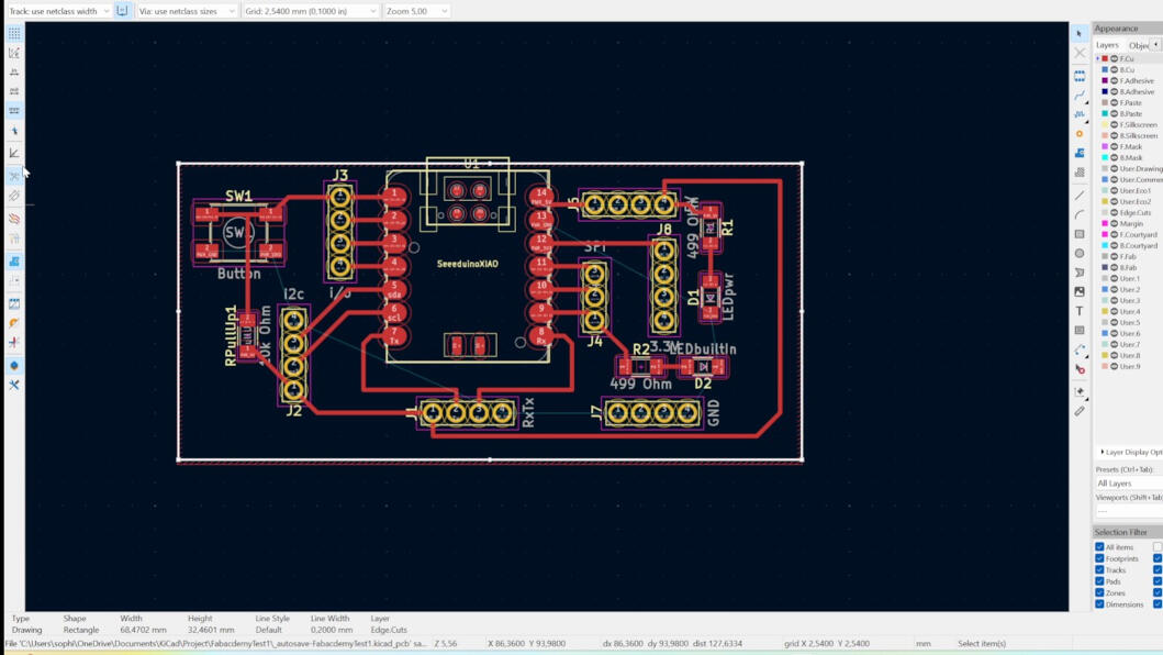
When dealing with the USB connection, it is crucial to position the edge behind the USB interface to ensure accessibility. This strategic placement ensures that the USB port remains easily reachable and facilitates seamless connection and disconnection of USB devices.
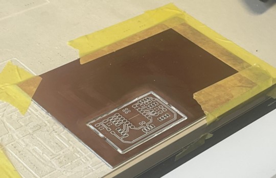
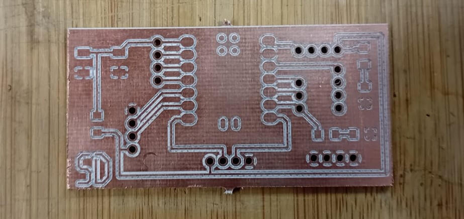
Milling
The export of the file and the control of the LPKF, that was used for the milling job, is described in the previous chapter. Here is the
finished milling job.
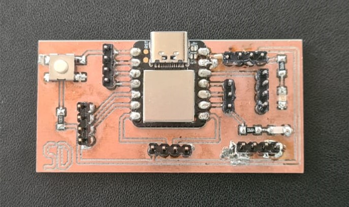
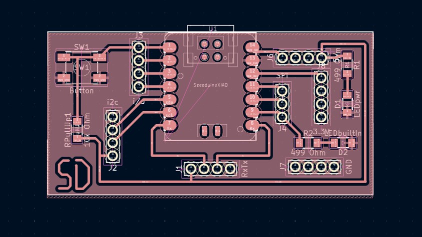
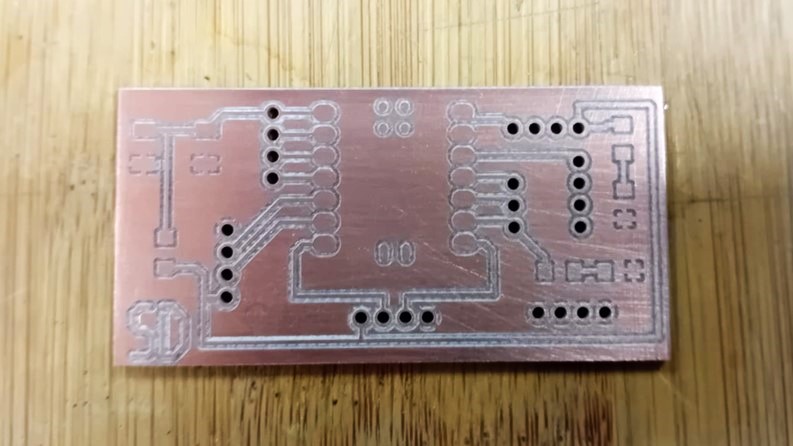
This is my finished design:
Soldering Components
Prior to commencing the soldering process, I meticulously cleaned the board using isopropanol. This step was essential to eliminate any contaminants, such as fingerprints, from the surface, ensuring an optimal soldering environment for improved adhesion and reliability.
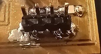
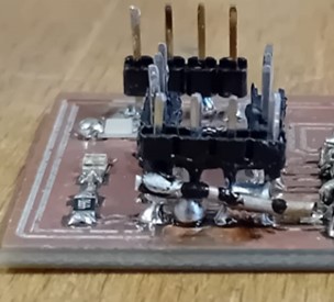
Initiating the stuffing with the microcontroller, my first step was to apply a modest amount of solder on the board to secure the microcontroller in the correct position. Unfortunately, a mistake occurred as I inadvertently used too much solder, causing the microcontroller to be slightly elevated on one side. This posed a challenge during the subsequent pin soldering, as the excess solder prevented the gap from closing. To address this issue, I had to delicately remove the microcontroller, employing a desoldering pump to eliminate the excess solder. Undertaking the process again with a more judicious application of solder proved successful. During the soldering, I initially used Tin-Nickel alloy, but encountered difficulties as it did not flow adequately into the gaps, complicating the soldering process. Recognizing this, I transitioned to using Tin-Copper alloy, which proved more effective in achieving proper soldering results.
Following the microcontroller, I proceeded to work on the resistors and LEDs. To ensure proper LED orientation, I employed the diode mode on the multimeter, which helped identify the correct direction. Progressing to the button, I found the assembly process to be smoother, and my soldering technique appeared to have improved, resulting in a neater finish compared to the earlier work on the microcontroller. But then, I tried to solder the pins. (ㆆ_ㆆ)
I encountered various challenges while soldering the pins onto the PCB. Following the guidance of our local instructor, I began by soldering them on the top, starting with one of the edge pins, ensuring the long end is aligned with the drill holes. To minimize the risk of damaging the board, especially given the prevalence of ground connections, I initially worked on the ground pins.
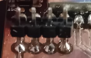
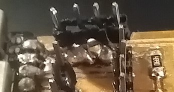
On the microcontroller's right side, where the pins were closely spaced, I encountered further challenges. The proximity of the pins made reaching them with the iron challenging, resulting in unintentional melting of the plastic around the pins. These difficulties underscored the importance of precision and patience (the lack of the last one is my personal issue with soldering (⩺_⩹)) in soldering intricate components like microcontroller pins.
Testing
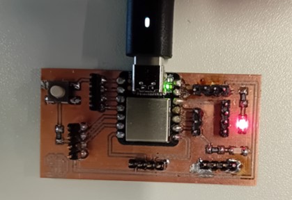
For testing, I first used the continuity test with the multimeter. After checking for any unwanted connection between paths and the ground. As every path was connected as wished. I continued with a power test. I connected the microcontroller to a power outlet and looked for the light of the power led. It worked!
The next thing was to test, if the microcontroller responds the uploading a program and to see if the pins, LEDs, and Button works. To start this process I used the Arduino IDE to upload code.
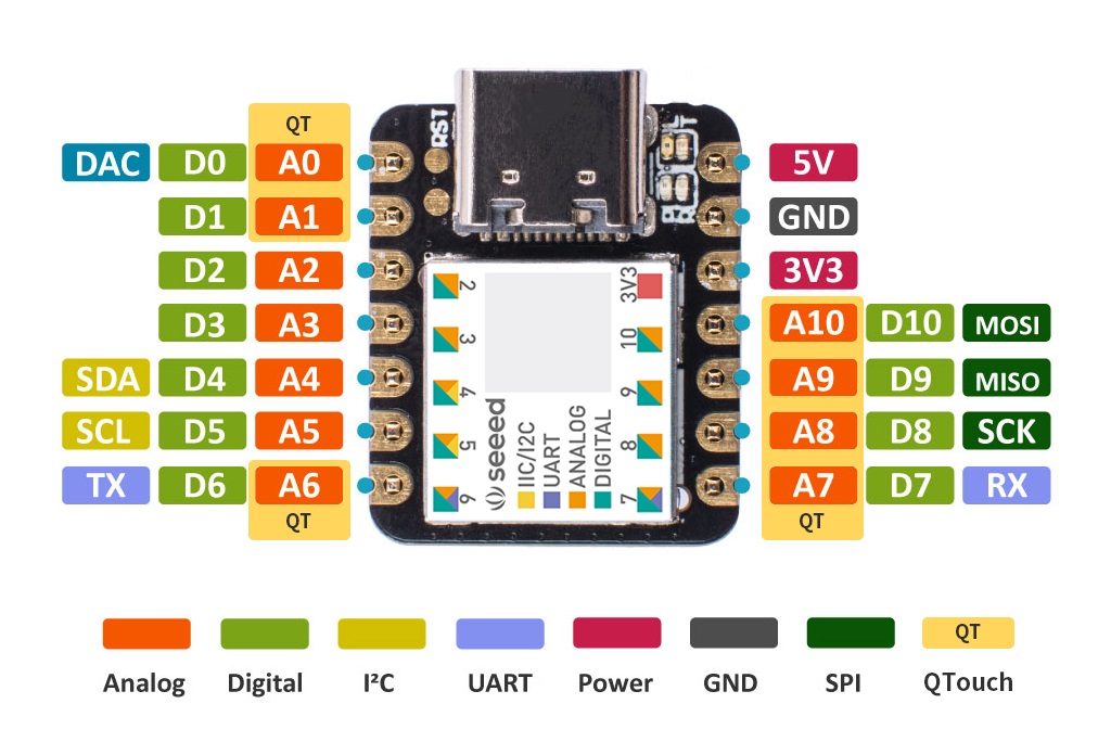
I started with the blinking test, which is a simple test to get the built-in LED to blink. Because of the hardware datasheet of th pinout. To start with it I needed to check if the Arduino IDE would recognize the board. It recognized the input USB port, but I had to install the type of board (SAMD). To do so:
- Go to "Files", click on "Preferences" and copy "https://files.seeedstudio.com/arduino/package_seeeduino_boards_index.json" into the tab "Additional Board Manager URL"
- Go to "tools", go to "boards", and click on board manager
- Search for SAMD
- Install "Seeed SAMD Boards"
- IGo to "tools", go to "boards", and select "Seeduino Xiao" as board
	// constants won't change. Used here to set a pin number:
	const int ledPin =  8;// the number of the LED pin

	// the setup function runs once when you press reset or power the board
	void setup() {
		// initialize digital pin LED_BUILTIN as an output.
		pinMode(ledPin, OUTPUT);
	}

	// the loop function runs over and over again forever
	void loop() {
		digitalWrite(ledPin, HIGH);   // turn the LED on (HIGH is the voltage level)
		delay(1000);                       // wait for a second
		digitalWrite(ledPin, LOW);    // turn the LED off by making the voltage LOW
		delay(1000);                       // wait for a second
	}
							const int buttonPin = 0;     // the number of the pushbutton pin
const int ledPin =  8;      // the number of the LED pin

int buttonState = 0;         // variable for reading the pushbutton status

void setup() {
  // initialize the LED pin as an output:
  pinMode(ledPin, OUTPUT);
  // initialize the pushbutton pin as an input:
  pinMode(buttonPin, INPUT);
}

void loop() {
  // read the state of the pushbutton value:
  buttonState = digitalRead(buttonPin);

  // check if the pushbutton is pressed. If it is, the buttonState is HIGH:
  if (buttonState == LOW) {
    // turn LED on:
    digitalWrite(ledPin, HIGH);
  } else {
    // turn LED off:
    digitalWrite(ledPin, LOW);
  }
}
Evaluation
Designing
The process of designing my first PCB was incredibly exciting. While there was the option to utilize pre-existing files from the Fabacademy webpage and our local instructor, I was personally driven to learn the intricacies of the design process myself. Despite the immense amount of information and the comprehensive day of learning, the experience was rewarding, emphasizing the depth of knowledge gained and the satisfaction of creating a design from start to finish.
Milling
The milling process proceeded smoothly, although there was an eagerness to experiment with the Roland machine alongside the LPKF. Despite the LPKF being more efficient and reliable, especially with its time-saving automated Z-leveling feature, the desire to explore alternative methods was present. A peculiar observation was that the LPKF typically performs a calibration routine by creating a small cut, measuring its width using its camera, and comparing it to the theoretical width. This calibration is crucial for the Z-leveling process. However, for reasons unknown, this calibration step did not occur for my PCB, though it did for my fellow group members. The discrepancy prompts a closer examination to identify any potential missed steps in the process that might have caused this deviation.
Soldering
Soldering proved to be a challenging task for me, exacerbated by the suboptimal tools and equipment available in the second lab on the alternate campus of Kamp-Lintfort. The soldering wire's thickness presented difficulties in reaching certain components, and the material appeared less viscous, hindering its ability to flow into gaps compared to the resources available in Kamp-Lintfort. Upon reflection, there are several changes I would make in a similar situation. I would opt to use the other lab, where conditions might be more conducive to successful soldering. Additionally, considering the challenges posed by the pin positions on the board, I would either solder the pins from the other side or strategically bend them to mitigate the risk of bending or breaking. Given the cumulative challenges faced during the process, I would contemplate milling the board again and starting the entire procedure afresh, implementing the lessons learned from the initial attempt.
Group Assignment
Accidentally, I undertook all the work without a precise understanding of the specific requirements for the group assignment versus those needed for the individual page. This confusion led to a blending of tasks, and I now recognize the need for a clearer distinction between the collective group effort and the individual contributions. Moving forward, I will seek better clarification to ensure a more focused and organized approach in balancing group and individual responsibilities.