Group Assignments
Group Assignment Link:
____________
Milling Group Assignment
Milling Overview and Group Assignment
"PCB milling, also know as mechanical etching, is the fastest, cleanest, high-performance and economical PCB prototyping process today." (- sourced from FlatCAM.org)
I was a bit behind on this weekly assignment as my instructors were away in other counties for training and the machines in-house were being serviced. I prepared over the weekend by learning as much as I could about building a circuit board and the components used. The milling process began on Monday.

The name of our machine is "DGSHAPE - Roland SRM-20". Oscar went through the process and intention of milling. Different types of milling tips / End Mills, such as "Ball End Mills & V-Bits".
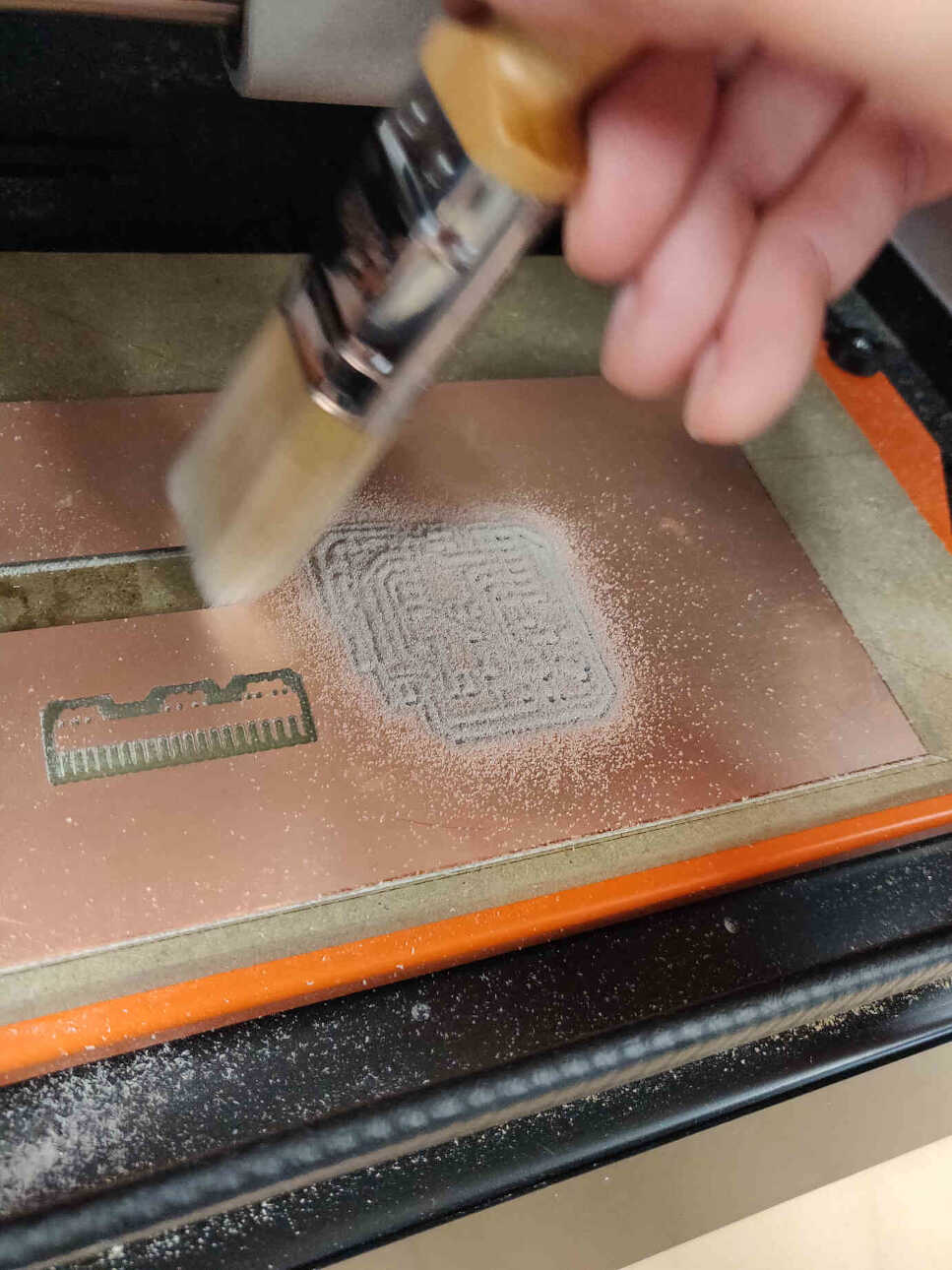
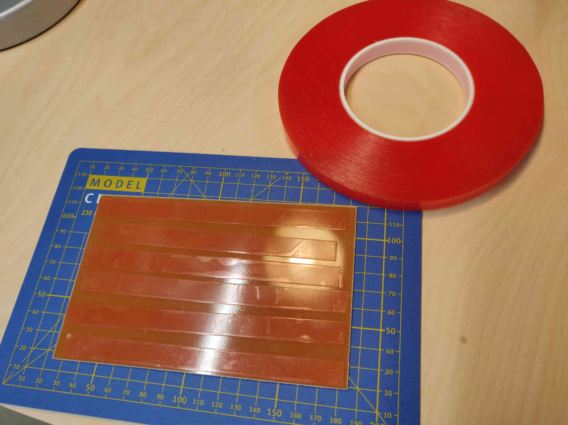
Acquire a Copper slate and put double sided tape on the back. Careful not to have any creases as it could affect the milling process by not being level. Also warned to make sure the slate is completely stuck down to the milling bed, especially when using the Ball End Mill as it could cause placement & design issues.
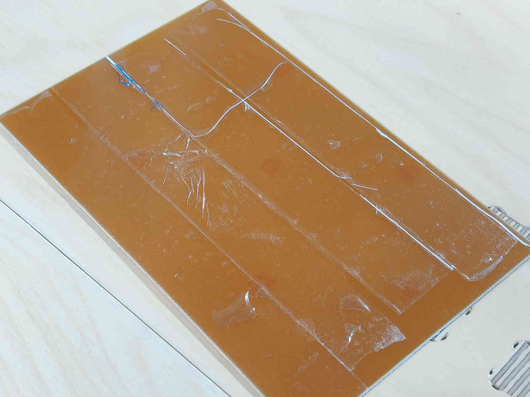
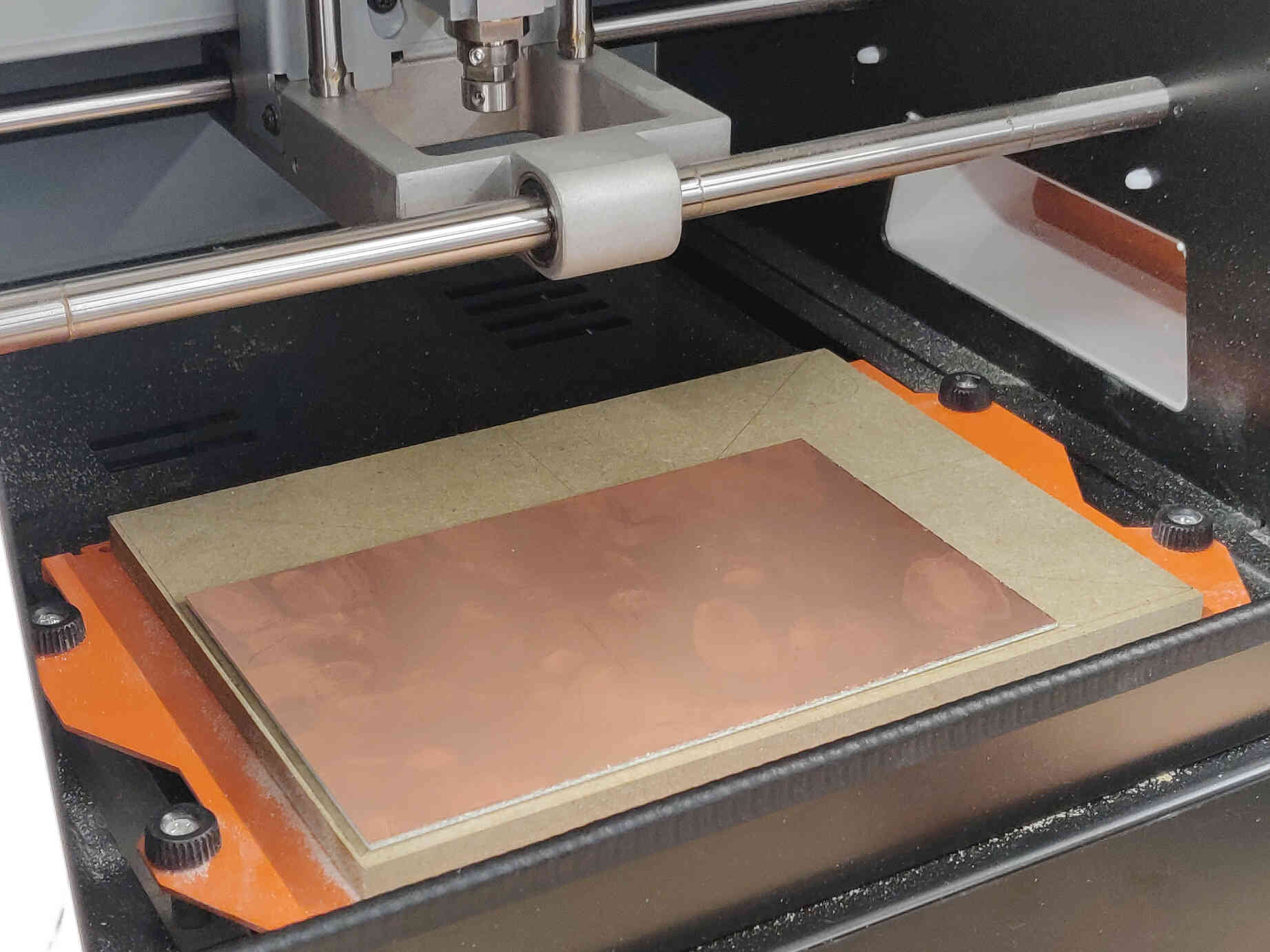
EDITOR'S NOTE: The image above shows you how the double sided tape should NOT be applied to the copper slate - it caused issues during our testing process as you will see. Avoid creases at all costs!!!
To remove copper from the intended areas, we will need to acquire a PNG or SVG file of the PCB's traces and outline designs. Then use thoses files to cut out the desired areas. For this we went to 'modsproject.org' which contained a full template on how to setup your milling path and acquiring the file needed for the milling machine.
____________
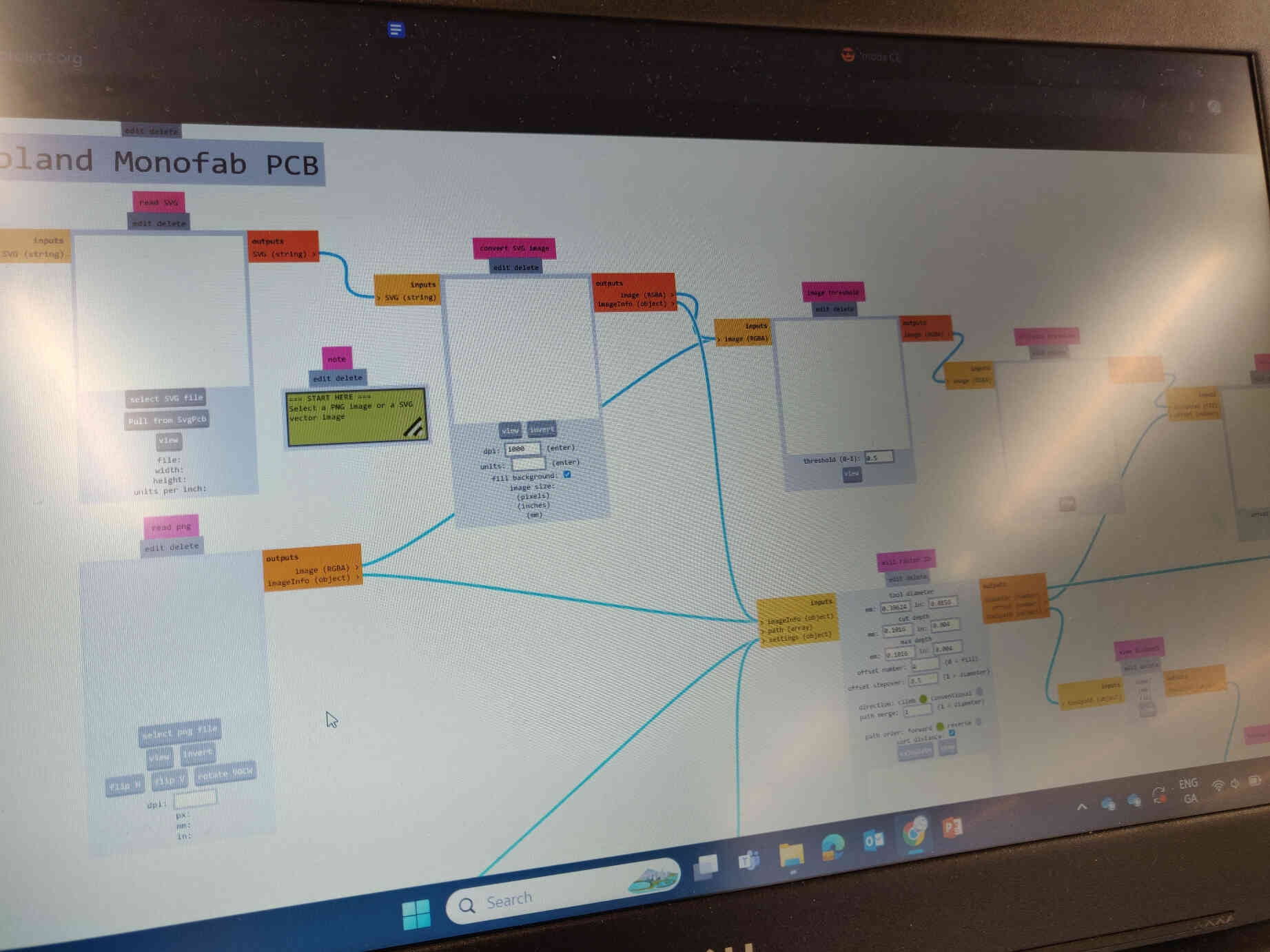
Modsproject.org and Preparing files for Milling.
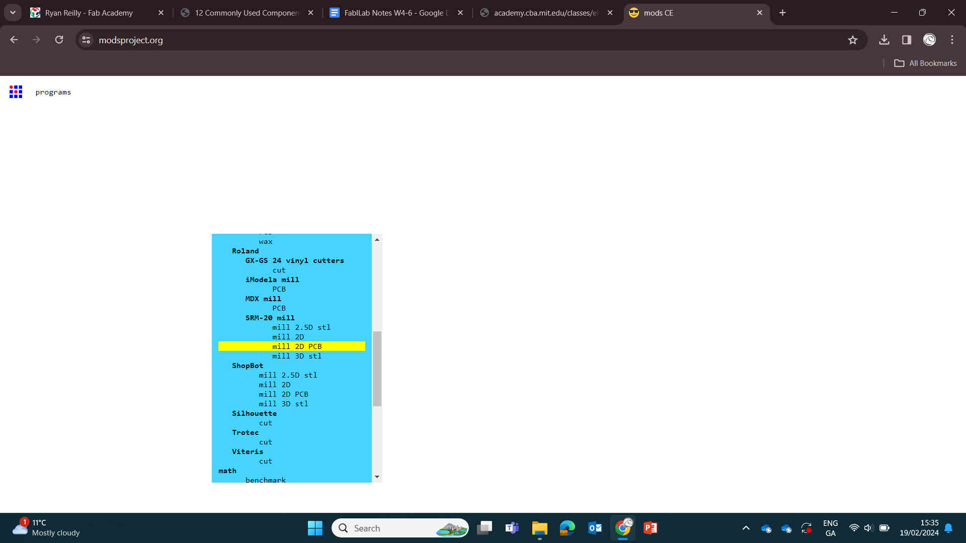

Before milling, we need to convert our design files into a language that the milling machine will understand. There is a site for doing just that! Click this link to be brought to Modsproject.org
Once on Site: Right Click -> Program -> Programmes -> Roland Mill MDX (PCB)

Milling Traces
Upload a PNG or SVG file of your traces design into the appropriate box (labelled 'read PNG' or 'read SVG' - We will go with SVG as those were the files that I would eventually use). Then in the box to the right (labelled 'convert SVG') click the 'invert' button.
When milling the traces, we use the 1/64 End Mill for a more delicate cut. So with our SVG file being for traces, we need to set the appropriate settings. Look below the convert box and you've see a box labelled "set PCB defaults". Click "mill traces (1/64)" button and it will set the template values. We will need to make a couple minor changes.
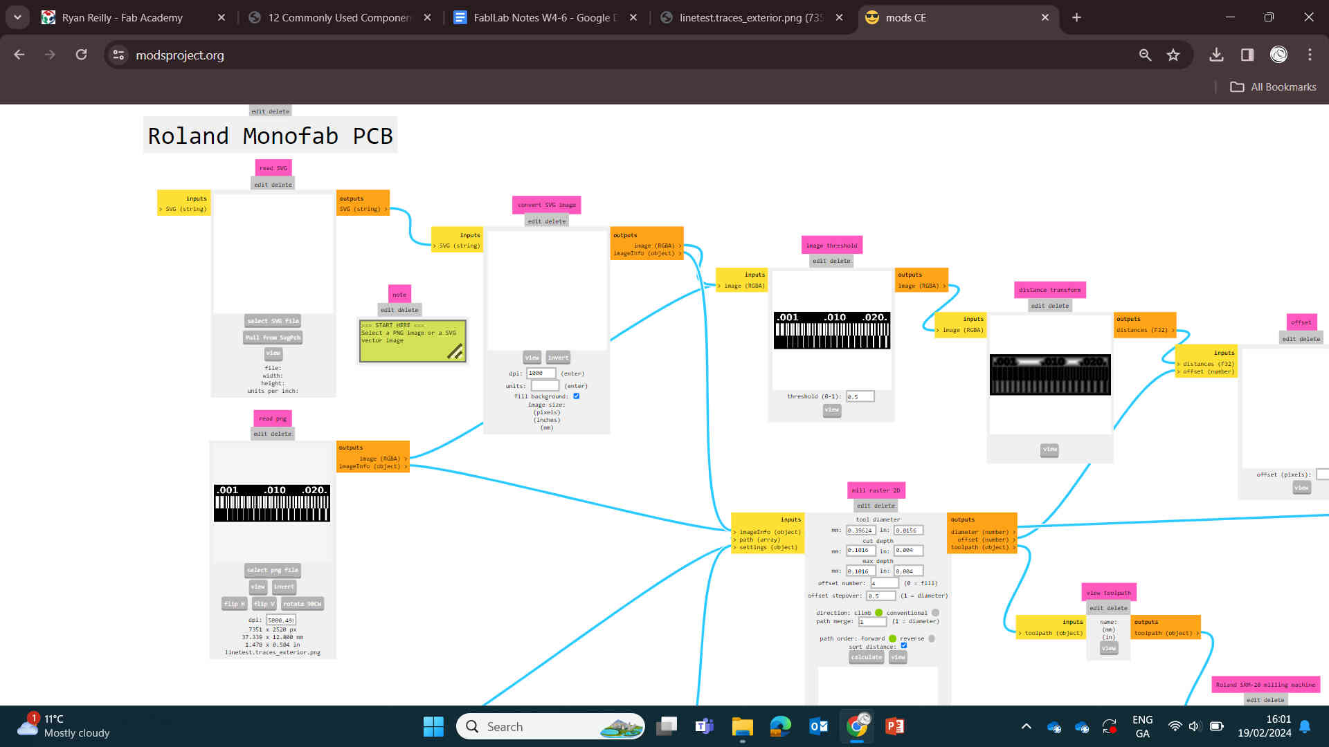
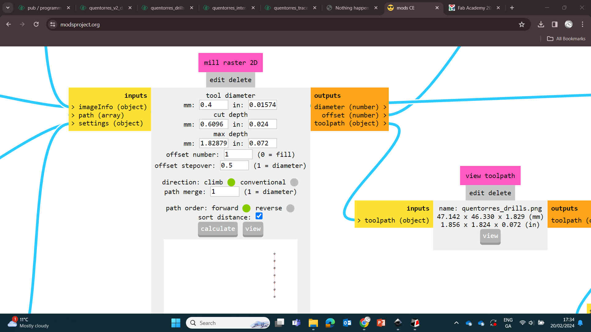
Navigate to the box labelled 'mill raster 2D' and change to these values ->
For milling traces:
Then in the box to the right labelled 'Roland MDX / iModela' change these values ->
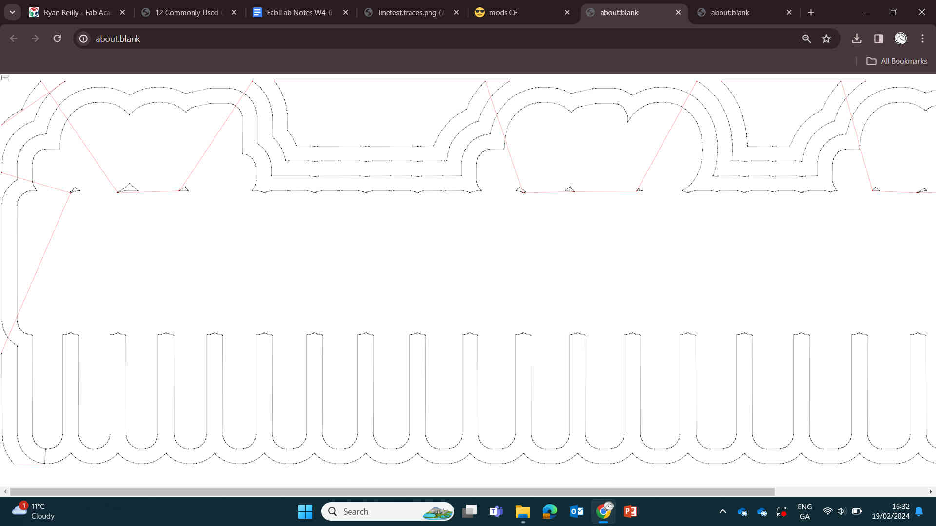
Then turn ON the node to the right that enables saving your files - labelled 'save file'. Once all that is set -> navigate back to the box labelled 'mill raster 2D' and hit 'Calculate' to convert/download your new file for milling and see the toolpath for your traces cut.
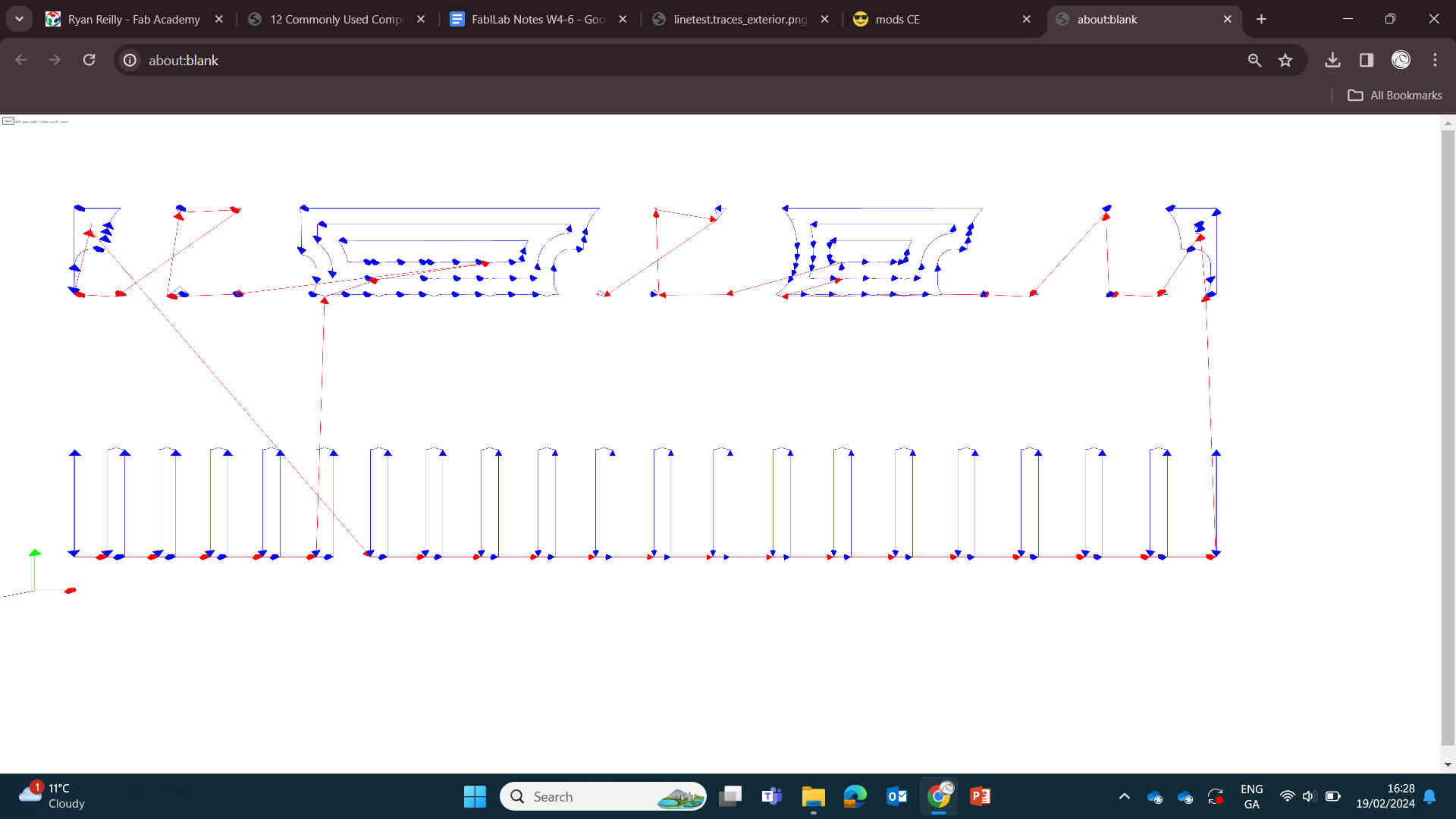
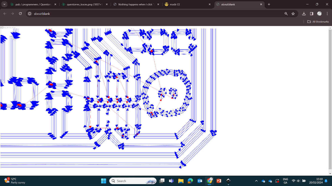
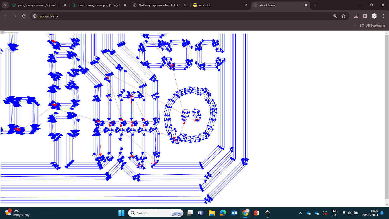
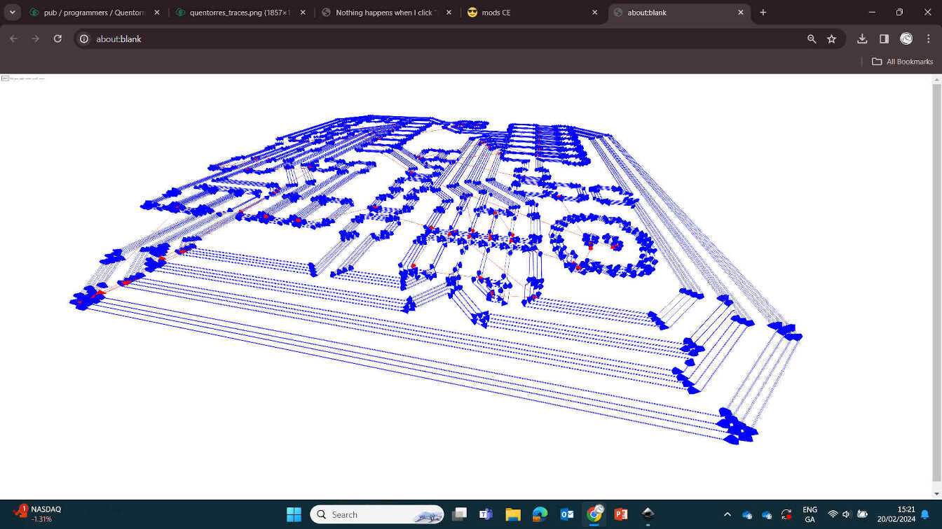
The toolpath will give a visual representation of the path the milling machine will take to cut out your design. From here you should be able to see that paths, cutting layers and if anything is out of place, such as missing outlines, unused edges, etc.
Before you start milling, it's best to convert the Outline file too. This is a similar process but with different values. It's important to get these values correct as End Mills are very very VERY easy to break, get strained or dulled.
Milling Outline
Upload your SVG file of your outline design into the appropriate box (labelled 'read SVG'). Then in the box to the right (labelled 'convert SVG') click the 'invert button.
When milling the outlines, we use the 1/32 End Mill for a thicker cut. So with our SVG file being for outlines, we need to set the appropriate settings. Look below the convert box and you've see a box labelled "set PCB defaults". Click "mill outline (1/32)" button and it will set the template values. Like before, we will need to make a couple minor changes.
Navigate to the box labelled 'mill raster 2D' and change to these values ->
For milling outlines:
Then in the box to the right labelled 'Roland MDX / iModela' change these values ->
EDITOR'S NOTE: There was some debate with the technician on whether the cut speed for outlines should be 1mm/s or 4mm/s. I ran both at seperate times and the 4mm/s was the much nicer cut and way faster than 1mm/s. However he explained that the end mill is more likely to break or get dulled out at 4mm/s. I would suggest speaking with your local technician for the correct setting for the right machine.
Then turn ON the node to the right that enables saving your files - labelled 'save file'. Once all that is set -> navigate back to the box labelled 'mill raster 2D' and hit 'Calculate' to convert/download your new file for milling and see the toolpath for your outline cuts.
Now that you have your files, connect your laptop to your milling machine via USB and open up 'VPanel'.
____________
VPanel and Milling
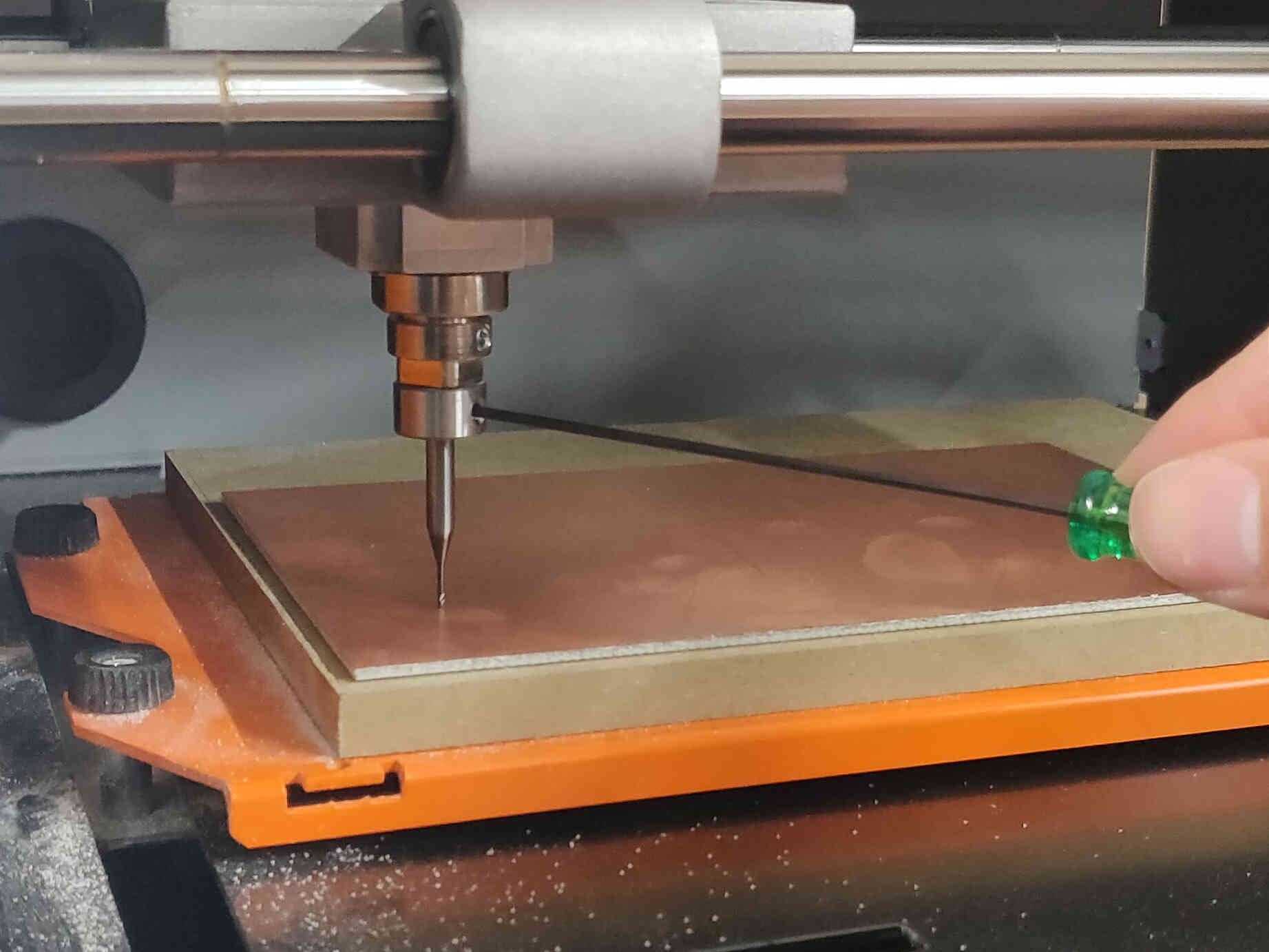

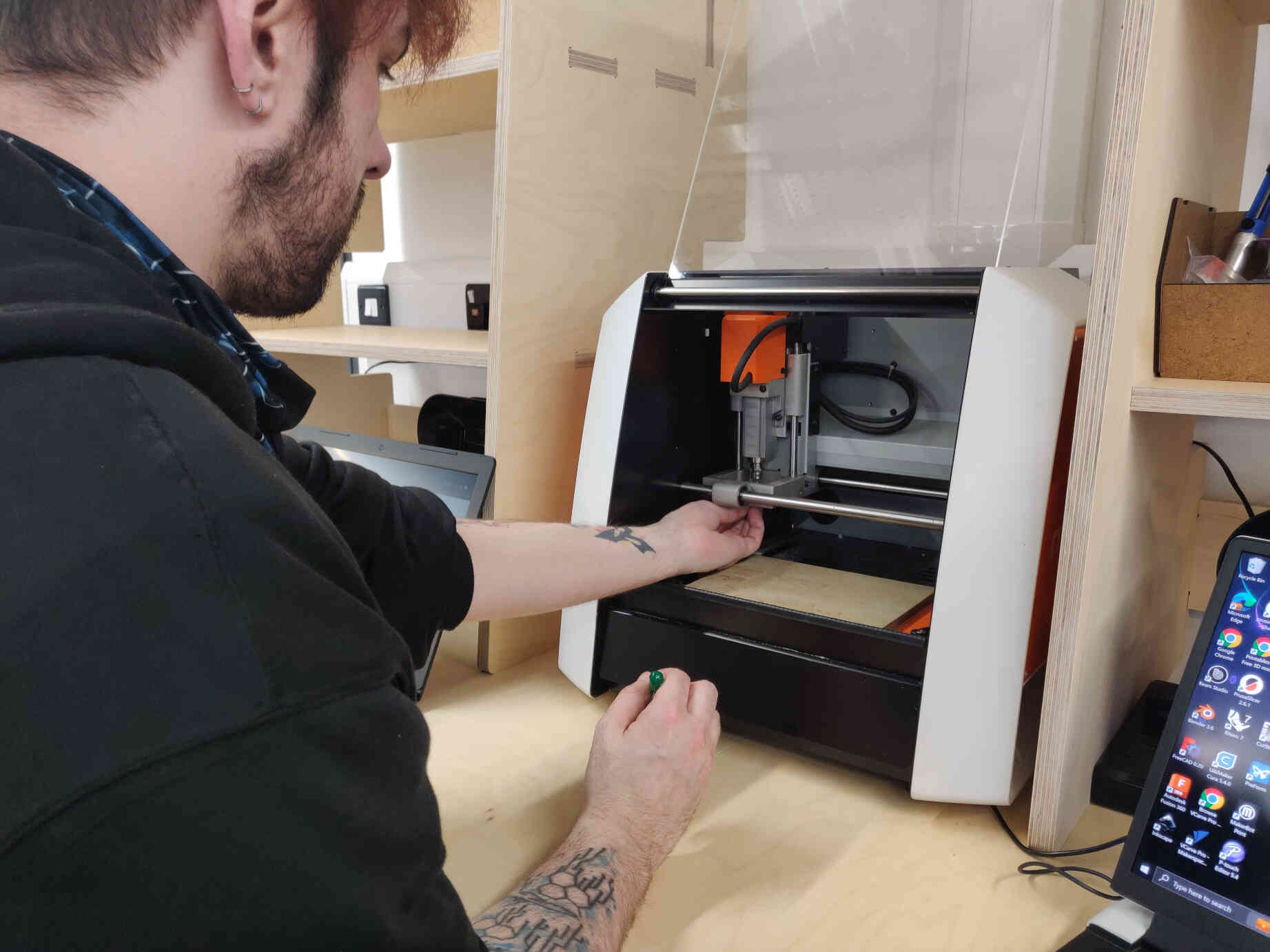
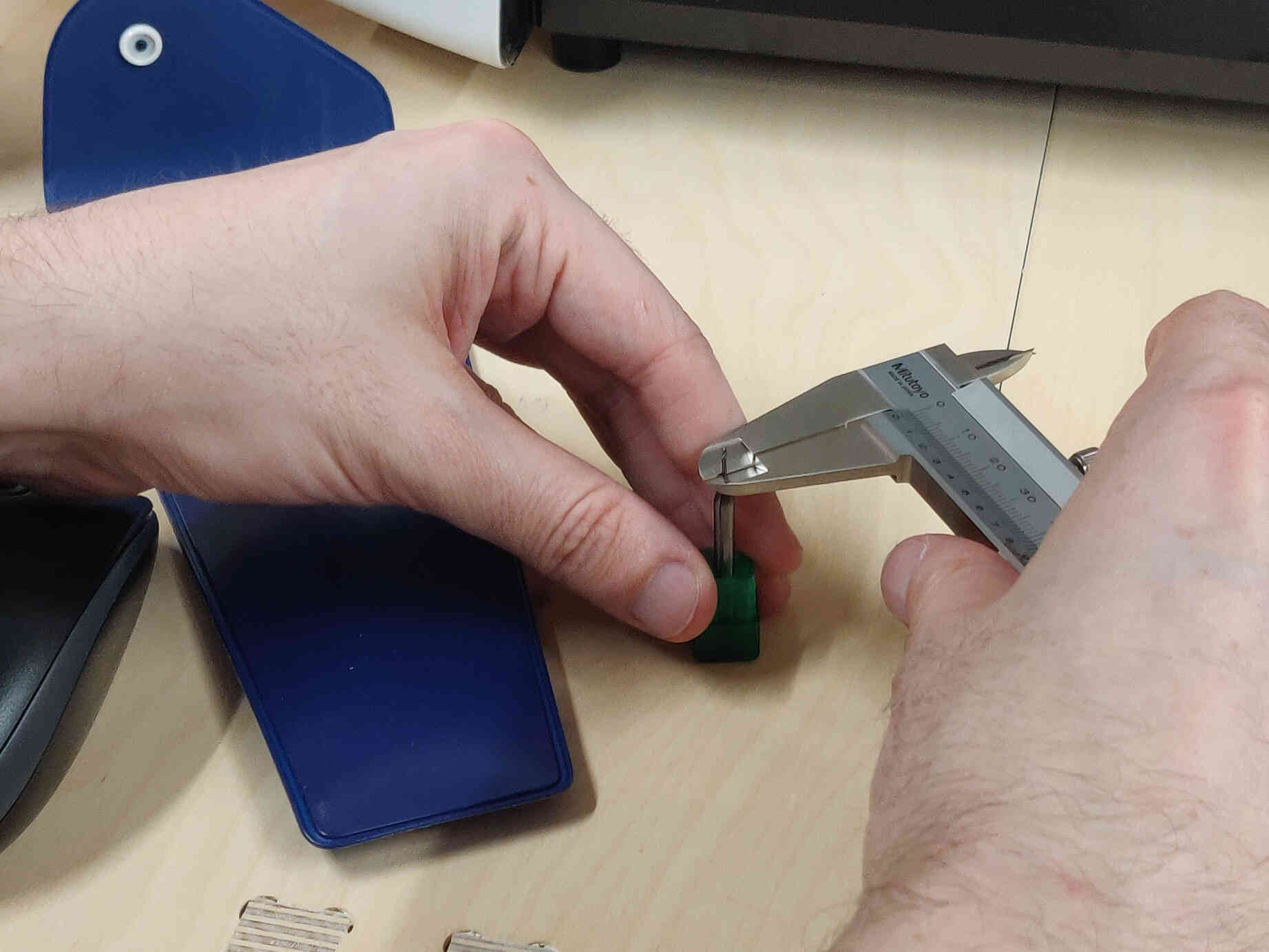
Once the design and slate are set and placed on the bottom left corner of the bed, I slotted & screwed in the End Mill. This is actually a delicate procedure as dropping the end mill on its head from even a couple inches can break your end mill. I've seen it happen twice from other users.
Then I was guided through controlling the machine's movements Axis via software called “VPanel”.
It's important to set the origin point appropriately and gently as moving the Z-Axis too far down & at a quick speed could snap the end mill tip, crack the copper slate and/or break the machine.

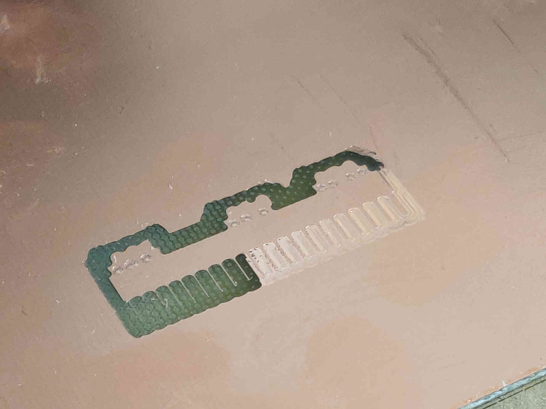
EDITOR'S NOTE: We ran a few tests of the group assignment example. The first run of the machine milled the left side of the test example and barely touched the right side of it. This could have been due the the copper slate being warped or the creases in the double sided tape.
For our second troubleshooting test, we went back into Modsproject.org and set the Z-Axis offset to +0.1, hoping it would reach the right hand side. We had to stop the process midway as it clearly wasn't enough. Going back to set the Z-Axis offset to +0.2, we ran the machine ago and it just about scratched the surface of the right hand side.
We ran one more troubleshooting test and set it the Z-Axis offset to +0.5. This setting finally cut through the slate on all sides but the design was far from ideal, cutting through a lot of the fine lines and barely showing the text. As the end-result was less than passable, we closed up the lab and left it for the next day - where I found the values as described previously.


With the correct values in hand, we set about finishing the Group Assignment, as you can see below.
We also went through a quick Overview of Quentorres Milling & Soldering. Once complete, my instructor gave me the Quentorres to practice soldering on. I enjoyed the process and got used to it quickly - though I also discovered the importance of keeping your soldering tip clean as the upper half of the tip was barely heating up.
____________
Individual Assignments
____________
Wednesday Meeting Reflection
This week we are moving on to 'Electronics Production', where we are expected to learn how to build a PCB (Circuit Board) from scratch and personalize it. I know literally nothing about circuit boards apart from doing a standard Arduino 'Blink' test several years ago, so I'm starting this week with no prior knowledge on what I am supposed to do or where to start.
A PCB board is like a small compact version of links between an Arduino and Breadboard.
Note: Sharp corners are bad for reflections.
____________
Global Open Time
Due to me working in a Screen Print Studio, I was curious about Screen Printing the Circuit design using electroconductive ink. It's definitely a worthwhile endeavour, but as Oscar, Julian and Rico had engrained into my head, I should be focusing entirely on getting used to the Milling and Soldering method first, as these processes will return in more difficult and larger assignments down the line. If I have time to go for the Extra Credit mark of trying out two processes, Screen Printing the design still has potential - but only if I have time and are confident with milling and soldering.
Advice from Rico
“Avoid using too much solder to connect the components to the PCB pads...it is not necessary (for the most part). The goal is to make an electrical connection between the component and the PCB pad...where the component is adequately adhered to the PCB.”
Soldering order:
- Start with Microcontroller
- smallest and lowest to largest and highest components
- components closer to the center of the board...to components to the outside of the board”
____________
MY GOALS FOR THIS WEEK:
I need to discover & learn all components that I need and what Enterprise Fablab currently has.
Need to understand how to use the CNC machine and miling and soldering.
Plus: Try to program something if you have time.
Side Notes:
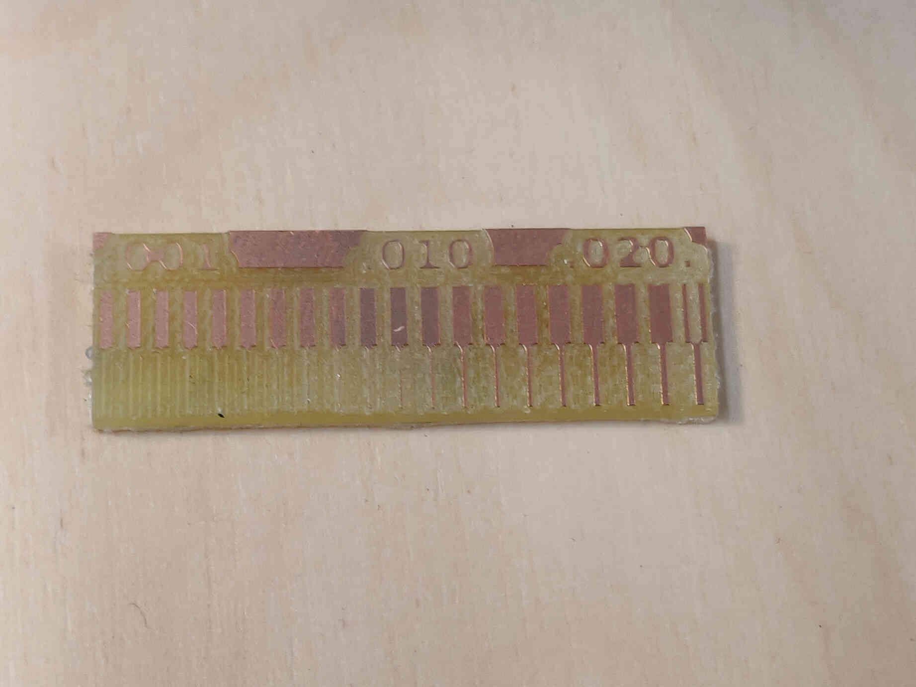
Bed levelling is critical when milling. They highly recommend using Flux, BUT you will need to clean up after you use it and make sure it’s dry before you plug it in. We are going to be Milling with FR1 / FR2 not FR4. If using FR4, you need to use a Hot Plate.
“Don’t cheap out on the solder”. - FabStudent with Experience.
“When using a png file. You should check the DPI. If wrong, (smaller than 700), It’s not working.”
____________
Arduino Basics
Components & Blink Test
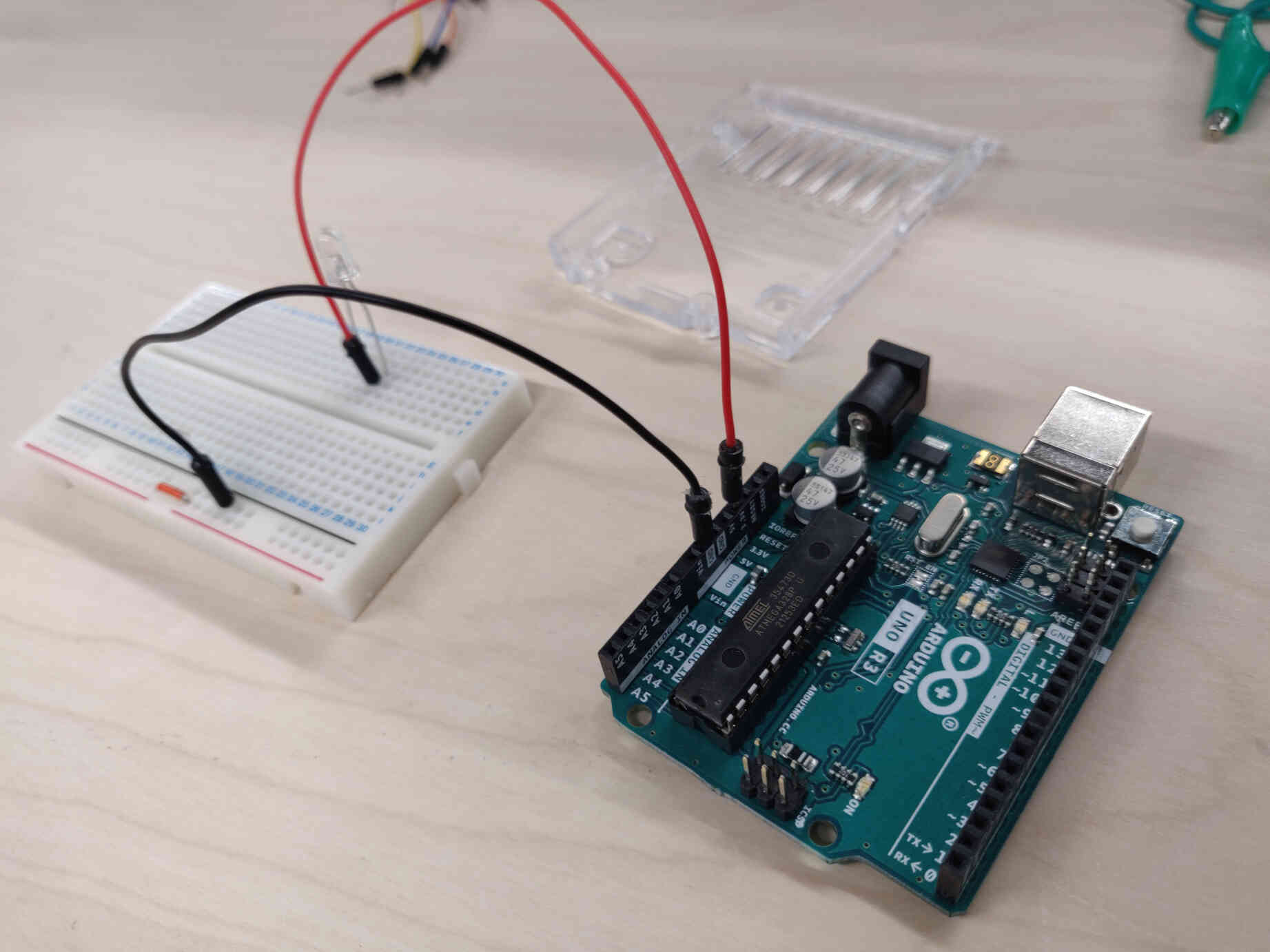
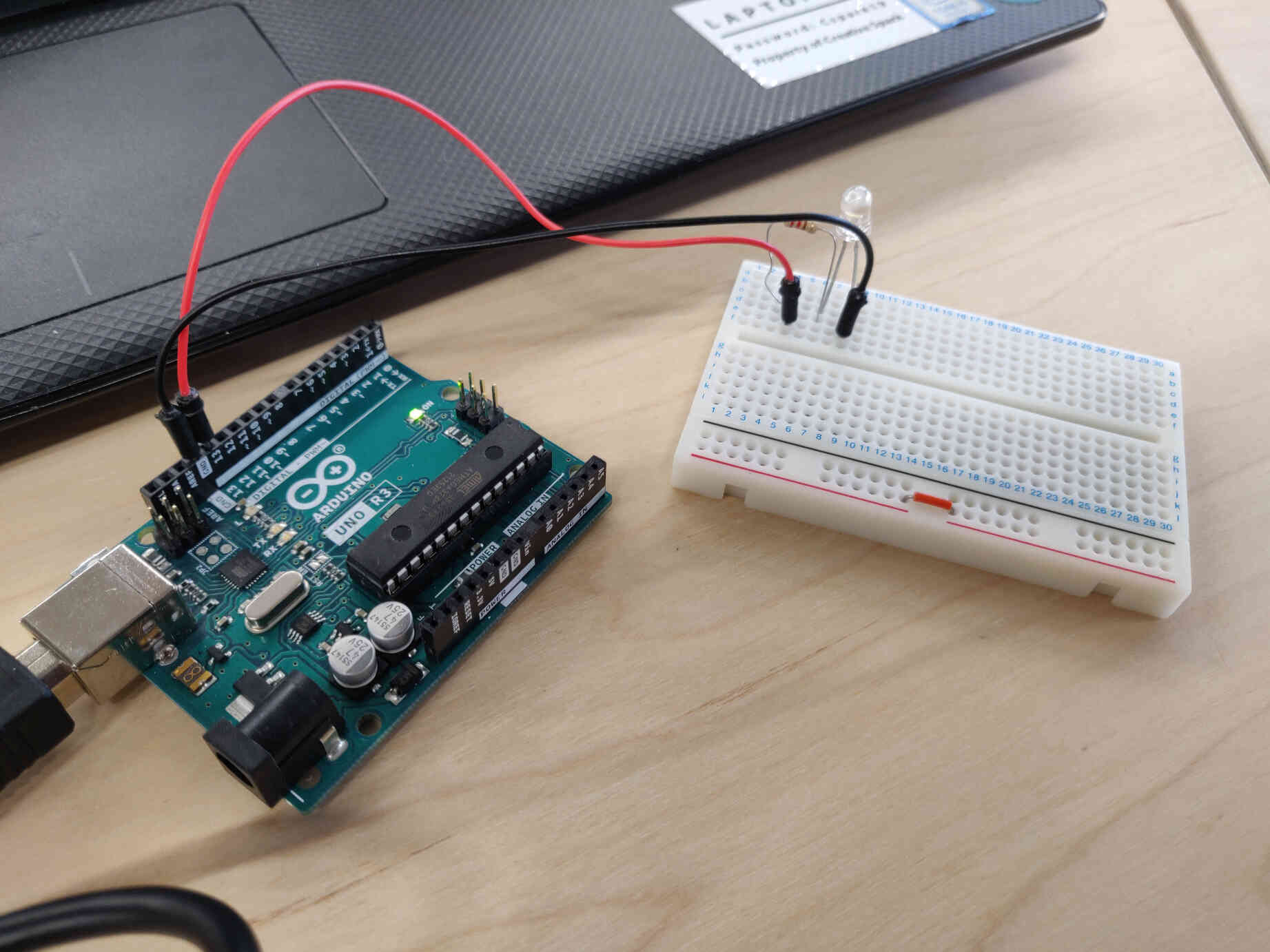
I went about taking stock of components I would need in Enterprise FabLab. Some components still needed to be organized & labeled, so we opened a new Arduino Uno box kit and was given a crash course on Arduino Uno. It took me a while to understand where the positives & negatives were coming from, and even after understanding the placements of components & wires on the breadboard, I still would mix up the correct positioning. (Positive & negative sides were reversed).

He started me off doing a Blink Test. Years ago in my 3rd year of college, we got Arduinos and performed/documentated around 8 types of Arduino tests back then, with the intention being to create a unique type of DIY controller that could play Guitar Hero. This was a whole ago and I barely understood it at the time so the refresher was definitely needed.
After placing an LED & Resistor component in the Breadboard and connecting the wires to the positives and negatives of the Arduino, I opened Arduino’s coding software and placed my Blink Test code. After verifying and uploading, I was able to perform the Blink Test of both the Arduino LED and the LED component.
Arduino IDE
Arduino IDE is an open-source coding platform that allows you to write code (C++) and upload the information to your PCB.

____________
Assignment: Milling a Circuit Board
Making the Quentorres PCB.
Work Area
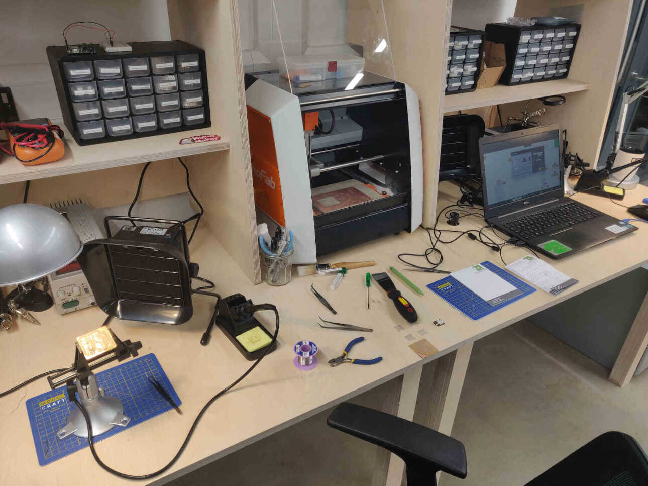
Everything was ready and set in place to complete my PCB.
I gathered and organised everything I needed:

I used Inkscape to add my custom design onto the PCB.
Exported as a PNG at 700dpi, then brought it in to Modsproject.org to adjust the settings for milling.

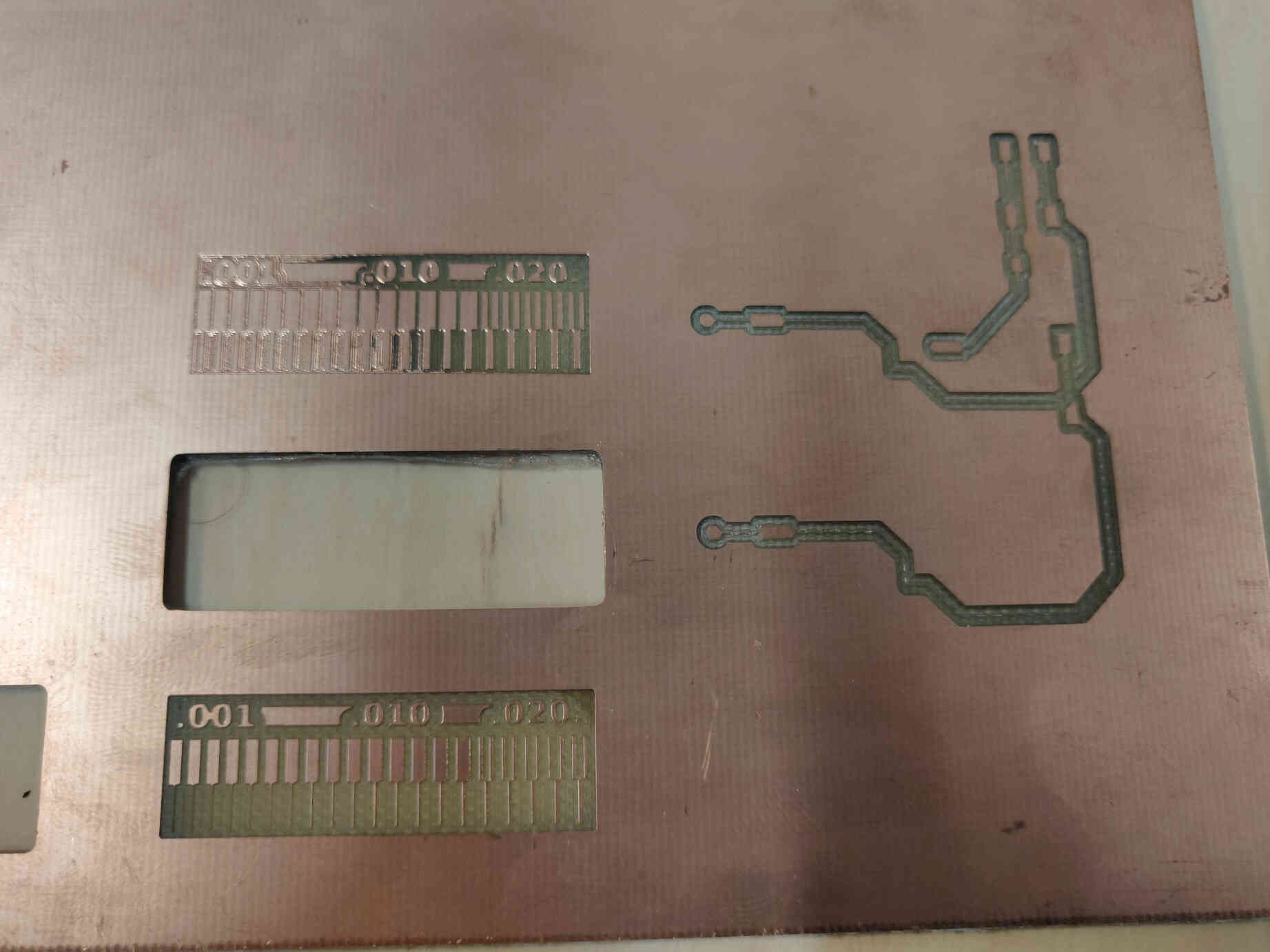
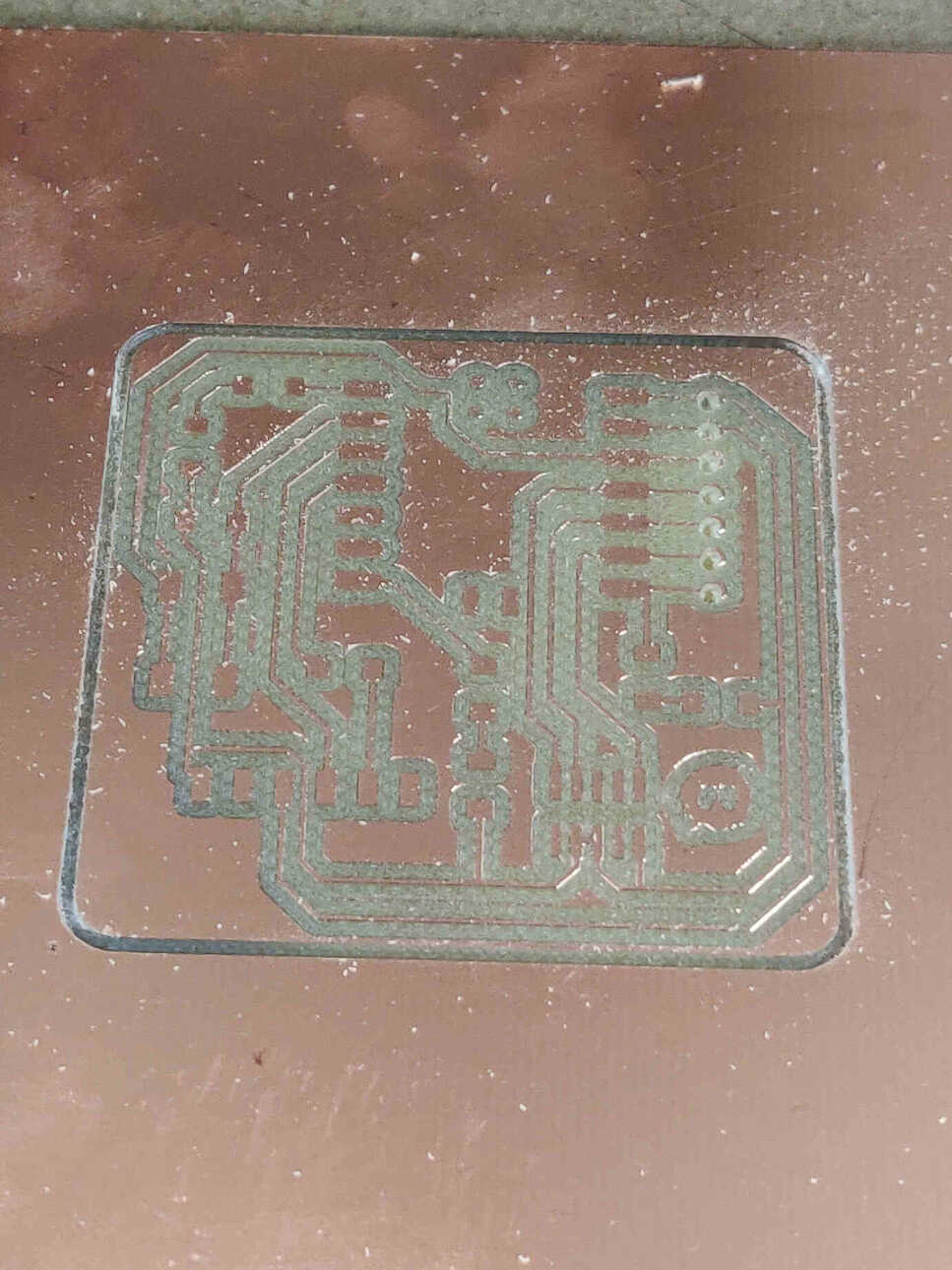
Milling Traces
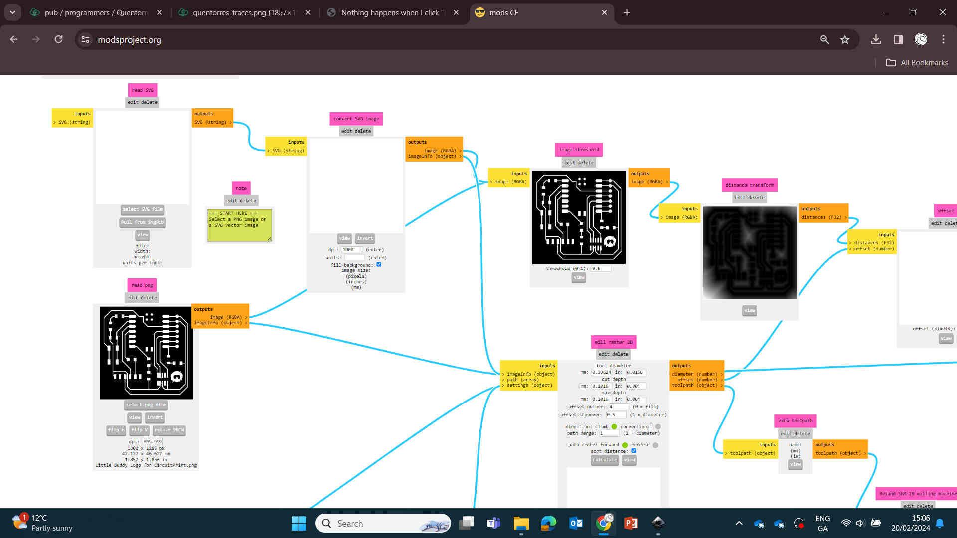

We uploaded the PNG file of our traces design into the appropriate box (labelled 'read PNG') Then in the box to the right clicked the 'invert' button.
When milling the traces, we use the 1/64 End Mill for a more delicate cut. With our PNG file being for traces, we need to set the appropriate settings. Below the convert box there's a box labelled "set PCB defaults". Clicked "mill traces (1/64)" button and it changed to the template values. We will need to make a couple minor changes.
In the box labelled 'mill raster 2D' we changed to these values ->
For milling traces:
Then in the box to the right labelled 'Roland MDX / iModela' changed these values ->
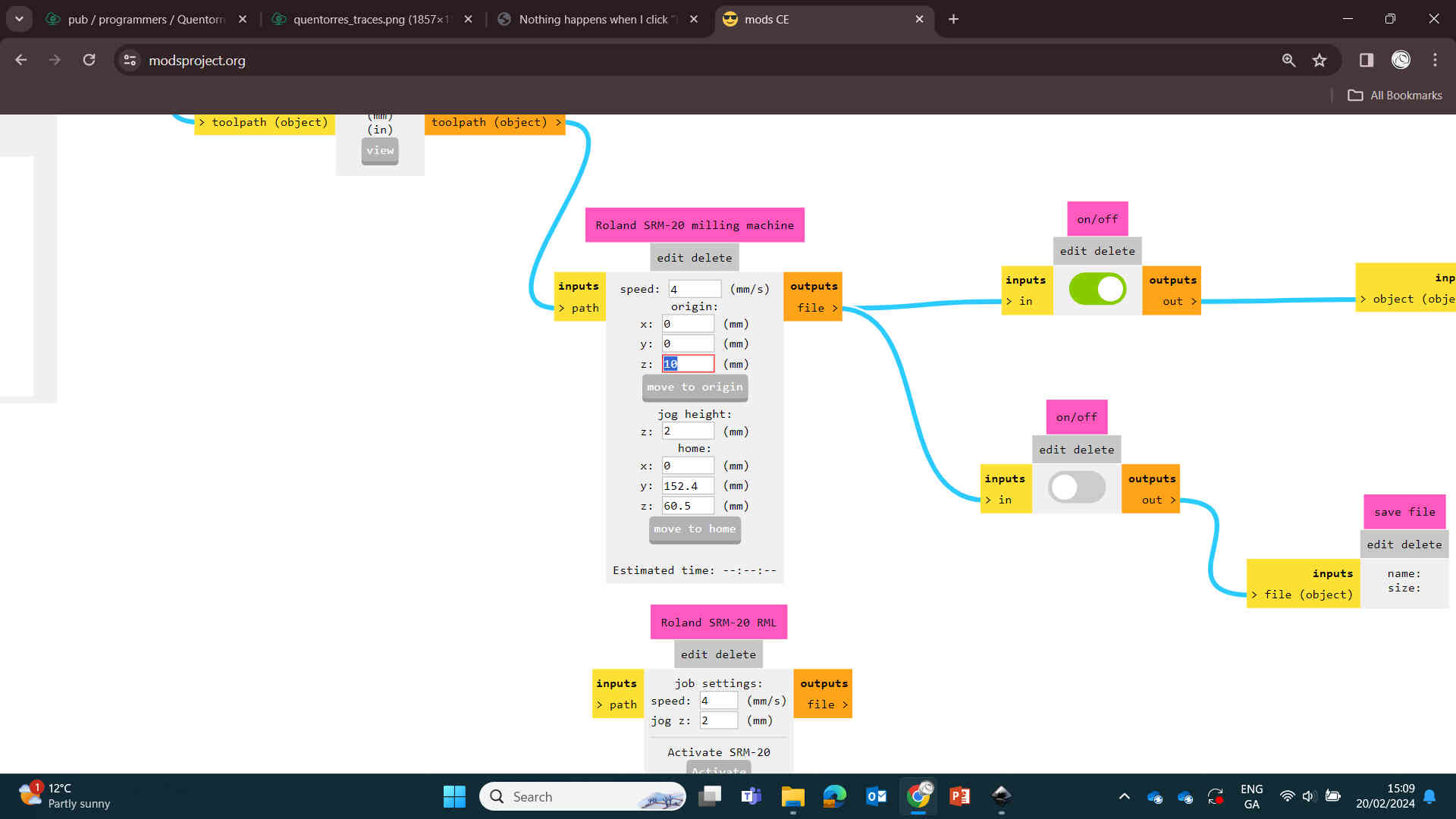
Then turned ON the node to the right that enables saving your files - labelled 'save file'. Once all that is set -> I navigate back to the box labelled 'mill raster 2D' and hit 'Calculate' to convert/download the new toolpath file for milling and saw the toolpath for the traces cut.
Before you start milling, it's best to convert the Outline file too. This is a similar process but with different values. It's important to get these values correct as End Mills are very very VERY easy to break, get strained or dulled.
Milling Outline
Uploaded our PNG file of the outline design into the appropriate box (labelled 'read PNG'). Then in the box to the right clicked the 'invert button.
When milling the outlines, we use the 1/32 End Mill for a thicker cut. So with our PNG file being for outlines, we need to set the appropriate settings. Look below the convert box and you'll see a box labelled "set PCB defaults". Click "mill outline (1/32)" button and it will set the template values. Like before, we will need to make a couple minor changes.
Navigating to the box labelled 'mill raster 2D' I changed to these values ->
For milling outlines:
Then in the box to the right labelled 'Roland MDX / iModela' change these values ->
EDITOR'S NOTE: There was some debate with the technician on whether the cut speed for outlines should be 1mm/s or 4mm/s. I ran both at seperate times and the 4mm/s was the much nicer cut and way faster than 1mm/s. However he explained that the end mill is more likely to break or get dulled out at 4mm/s. I would suggest speaking with your local technician for the correct setting for the right machine.
Then turned ON the node to the right that enables saving your files - labelled 'save file'. Once all that is set -> navigate back to the box labelled 'mill raster 2D' and hit 'Calculate' to convert/download your new file for milling and see the toolpath for your outline cuts.

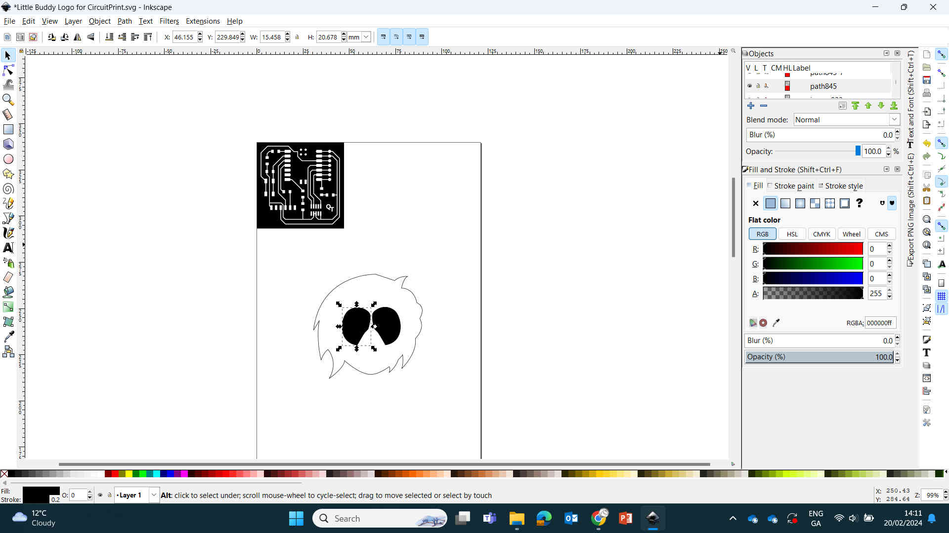
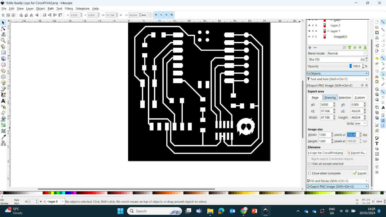
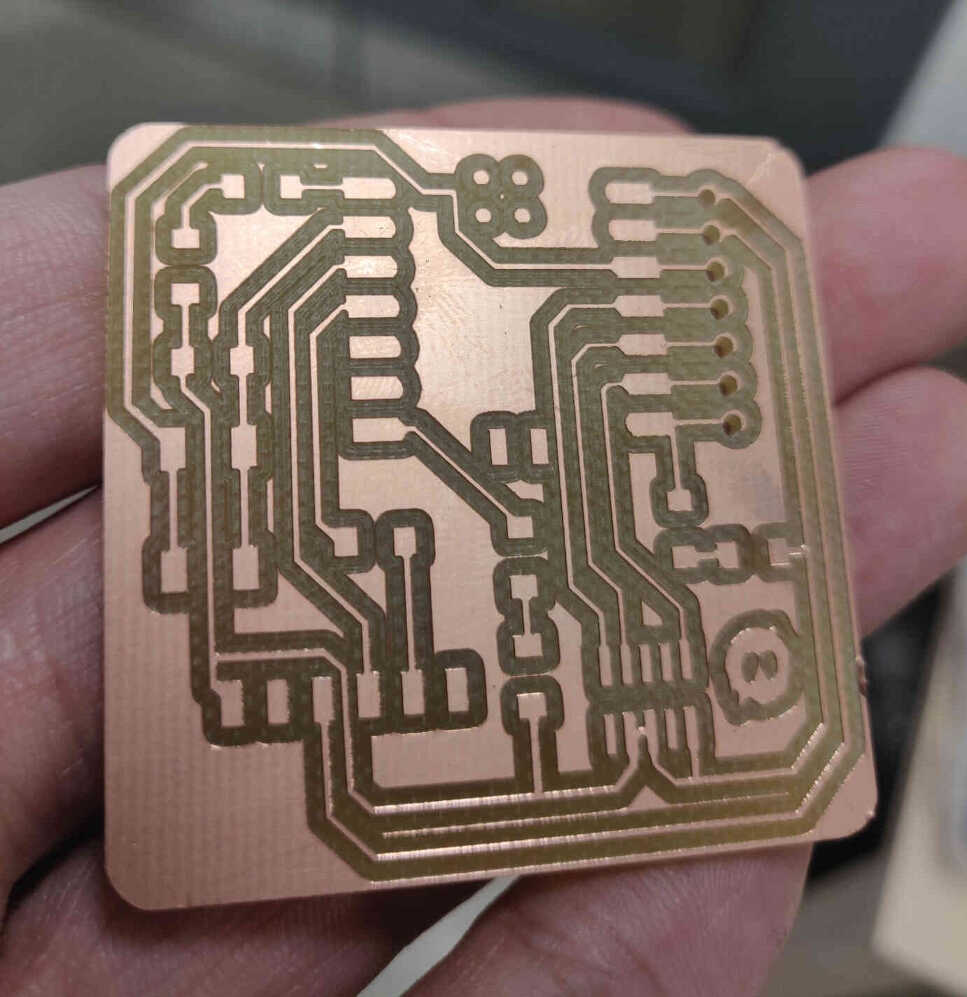
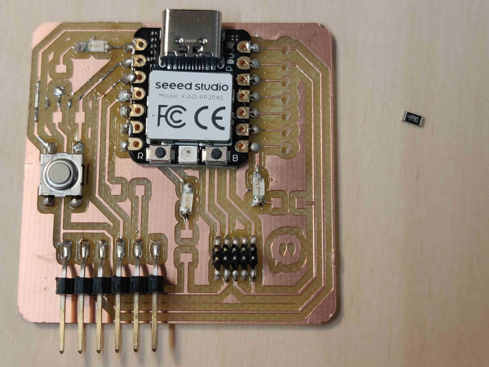
For the extra credit assignment, I took the PNG of the Quentorres Circuit Board into Inkscape, removed the QT logo by placing a square box on top of it, then imported my Little Buddy logo.
Had to adjust the scale of my logo in Inkscape as it was just about interrupting the milling path.
The toolpath gave a visual representation of the path the milling machine will take to cut out of the design. I needed to make slight adjustments back in Inkscape as my logo was getting too close to the traces. After scaling it down, I repeated the modsproject process and got my file.
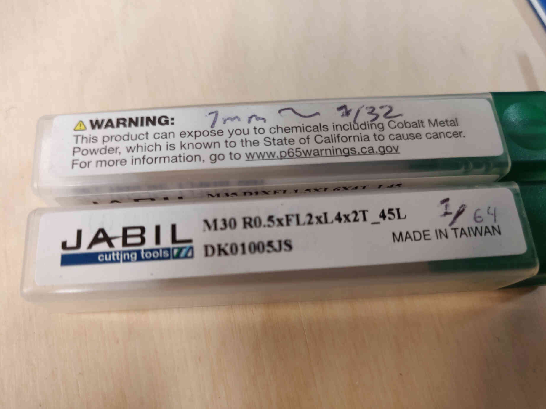
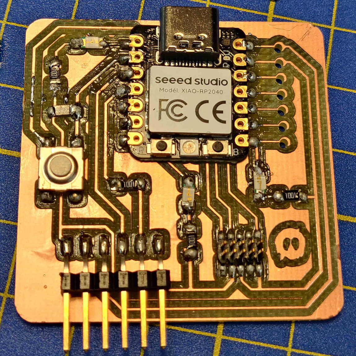
Once the design and slate are set and placed on the bottom left corner of the bed, I slotted & screwed in the 1/64 End Mill almost as far as the tip. Then I Set the X & Y Origin on VPanel near the bottom right of the slate. Then Lowered the Z-Axis as far as it would go - then raised it by 5.00mm and set the Z-Origin. This is to allow the end mill space to work. Failing this procedure before, it causes the end mill to tip the copper plate, the retreats back to the starting position as it can't go any further.
It's important to set the origin point appropriately and gently as moving the Z-Axis too far down & at a quick speed could snap the end mill tip, crack the copper slate and/or break the machine.
Then I unscrewed the End Mill and VERY GENTLY lowered it down to touch the copper plate - then tightened it again. This is actually a delicate procedure as dropping the end mill on its head from even a couple inches can break your end mill. I've seen it happen twice from other users.
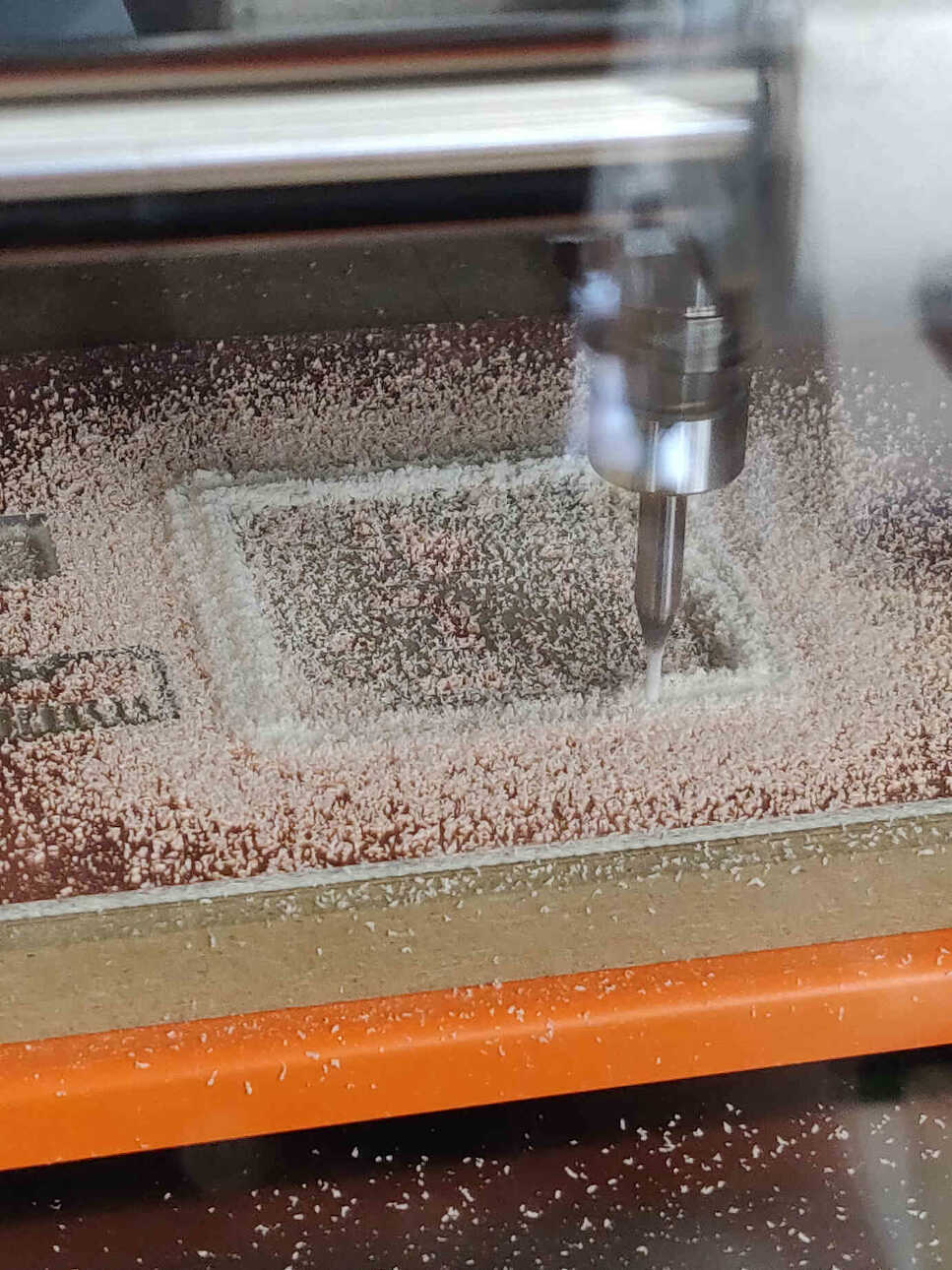


Bring your traces file into VPanel and start the cut. The spindle will run roughly at 6000RPM.
Repeat the above process for the Outline file.
Remember to swap out the 1/64 End mill for the 1/32 End mill!
Other Processes
The idea of using a lithographic process to create a Circuit Board interested me as I work in a Screen Printing Studio. I discussed the idea with Oscar and my employer in the Screen Printing Studio, and they suggested I could screen print the traces/paths of the circuit board using electro conductive ink. I brought this up to Julian and Rico during the Saturday Global Open meeting and they strongly suggested before I try any other process, to try and get accustomed to the Milling & Soldering process as we will be continuing to use this process on bigger projects in a few weeks. I took the advice to heart and focused entirely on building a circuit board.
____________
Soldering the PCB
After milling the circuit design onto the copper plating, I now had to gather the correct necessary components needed to build this working PCB. I was advised to write down a list of all the components I need (with pen & paper) so that I can place each component next to their listed counterparts and sellotape them down so that they wouldn’t be shaken off to the floor if moved.
It took some guidance to find all the necessary components as so are not so obvious to someone as new to this as I am - even when correctly.
Once I retrieved all my necessary components, Oscar gave me a few tips on soldering safety and gave me a Quentorres that he milled to practice on. This was also my first time ever soldering. For practice I attempted to solder some metal onto each and every spot that could hold it while trying to achieve a ‘shiny and smooth’ result. I was advised to have the PCB clamped down using a ‘Panavice’ clamp, but I found this very difficult and frustrating with my shaky hands.
I much preferred soldering with the PCB flat on the table - with a protective mat under it… which may or may not have been damaged in the process. Good lighting from a nearby lamp and tweezers for tiny components were also necessary. I found the soldering process intense but oddly relaxing and satisfying once a near-perfect soldering was achieved.
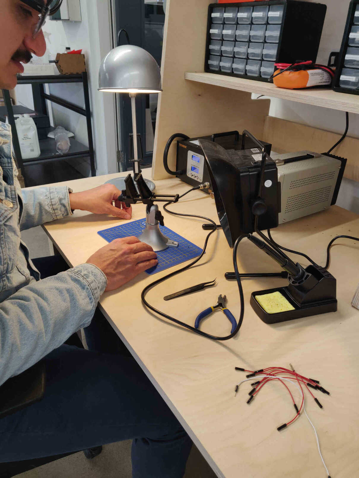

Soldering Tips
To solder, I needed a soldering tool along with a string of ‘Rosin Core Solder Wire’. You can turn on the soldering machine and set the heat to roughly 350 - 380 degrees. I was told from Fab Academy and several soldering videos on YouTube that its good practice to place the solder tip onto the copper slot that you want to solder to heat it up. After a couple seconds, slightly press the tip of the solder wire against the side of the soldering tool tip until it begins to melt. When it begins to melt, you can drag / slip the metal wire down the tip and onto the copper.
You can use both the wire and the soldering tool to maneuver and shape the melted metal into place. Keep in mind though that you only have a couple of seconds before the melted piece of metal instantly hardens again! This isn’t a problem as the solder tool tip can instantly melt and reshape the placed metal. However there was something odd about the soldering tools I was using - which I shall explain shortly.
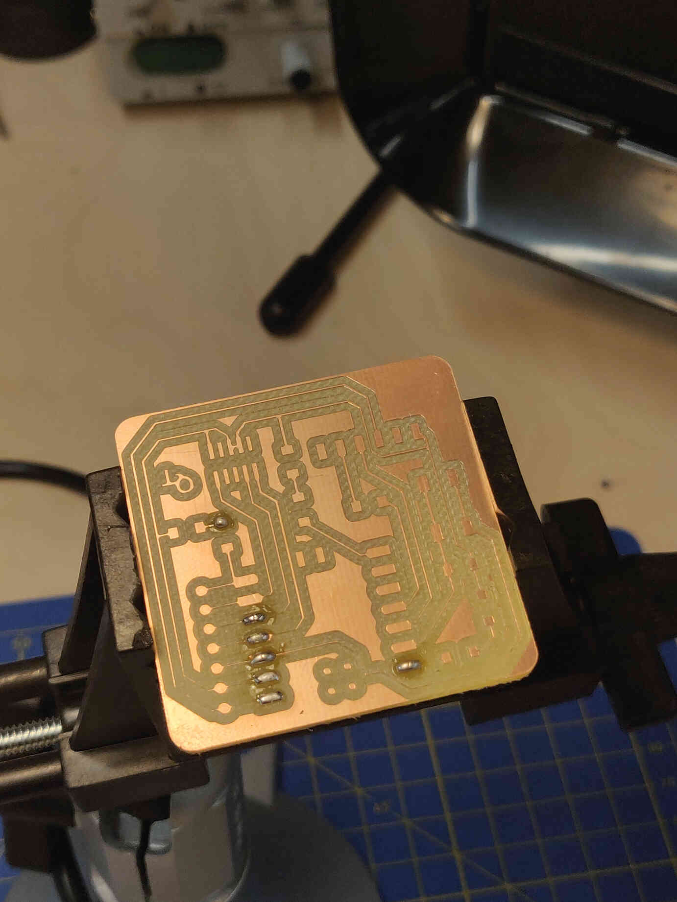
Satisfied with my soldering technique on the practice PCB, I prepared to solder components to my own PCB. This is where the process became increasingly different - with good reason. To start, I took Neil’s advice for soldering the microcontroller - to start soldering a small piece of metal onto the intended copper plate - preferably start from where the top left microcontroller pin will be placed. Once that’s done, position the microcontroller where it needs to be and re-solder the top left pin, shaping it so that the metal connects to the microcontroller pin and stays in a fixed position.
With this done, you’re free to solder down the rest of the pins individually. I also used this method for fixing every component into place.
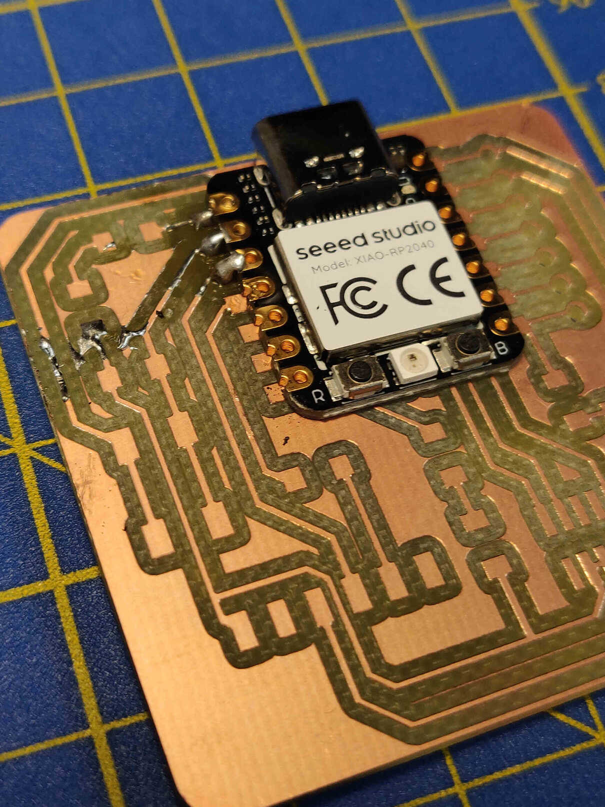
Started soldering componants onto my own PCB and ran into issues. Soldering equipment failure
Intensity and stress of placing and soldering such a tiny component was slightly exhilarating. I followed the images found in fab academy and placed each component exactly as I saw.
Quentoress Result (w/ custom logo!)
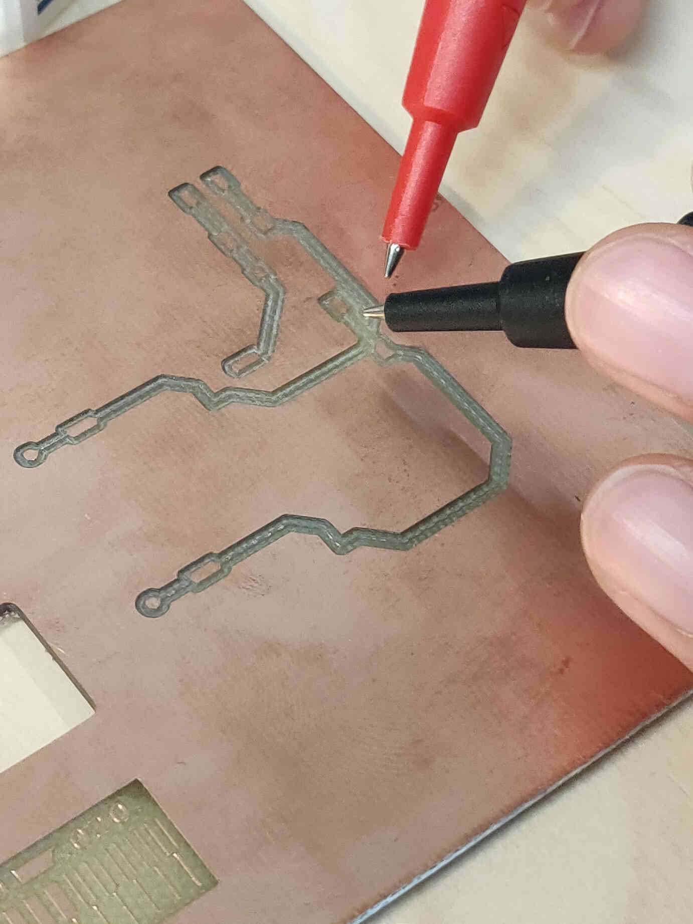
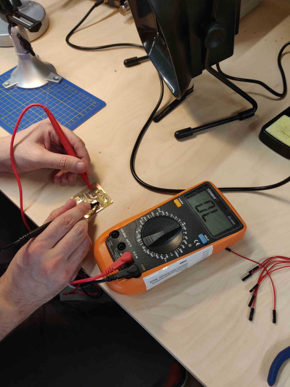
With the soldering finished, I needed to check if the electical current still runs smoothly. We can check the flow of the electrical current with a device called a Multimeter. With the 2 prongs touching both sides of a connection, I was able to demonstrate the flow of the electric current by whether the device makes a 'beep' noise when touch opposing sides - and if the noise is consistent! I tested the electrical connections. Some weak connections but each seem to be working / connecting without any faulty lines.
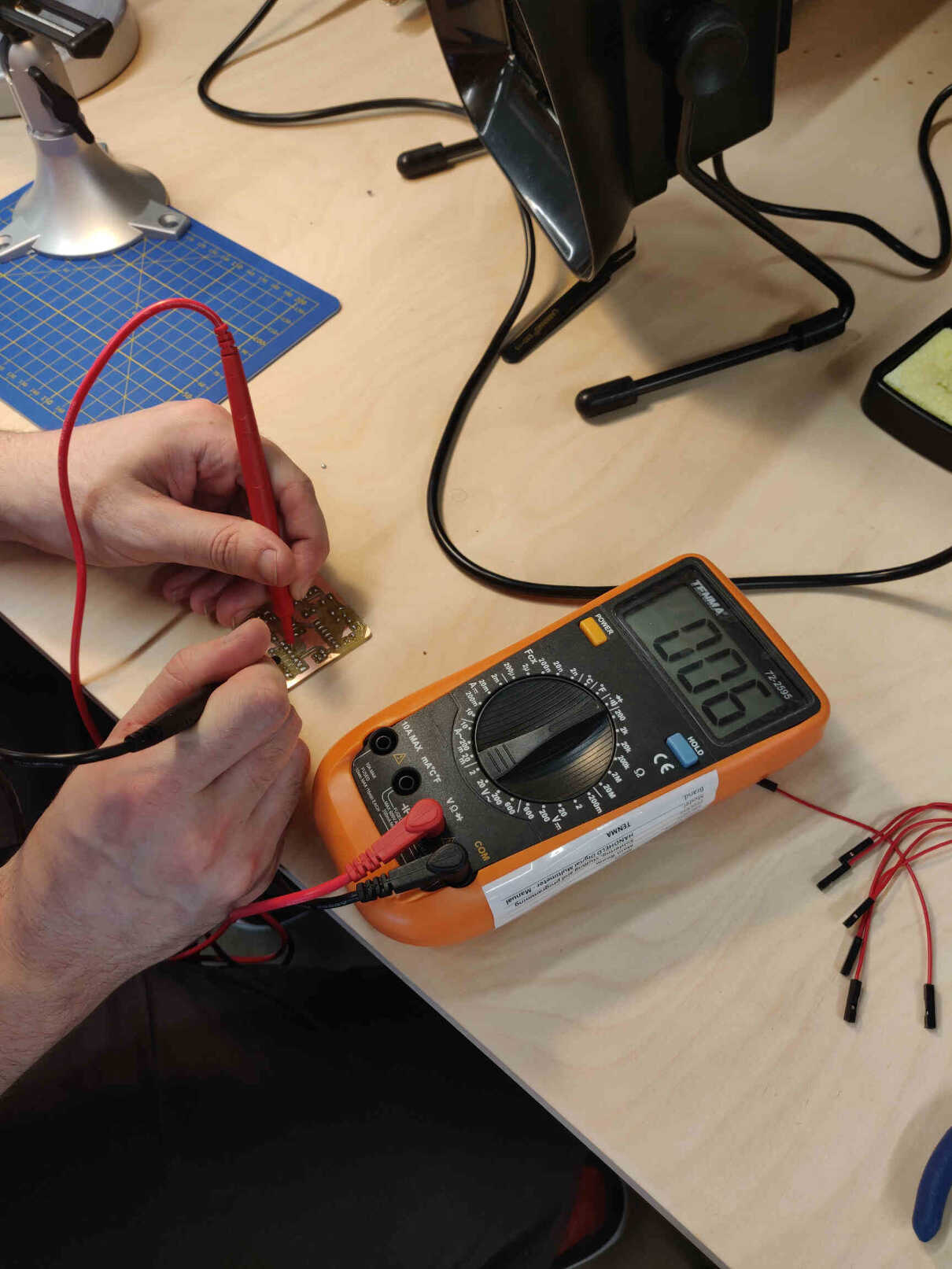
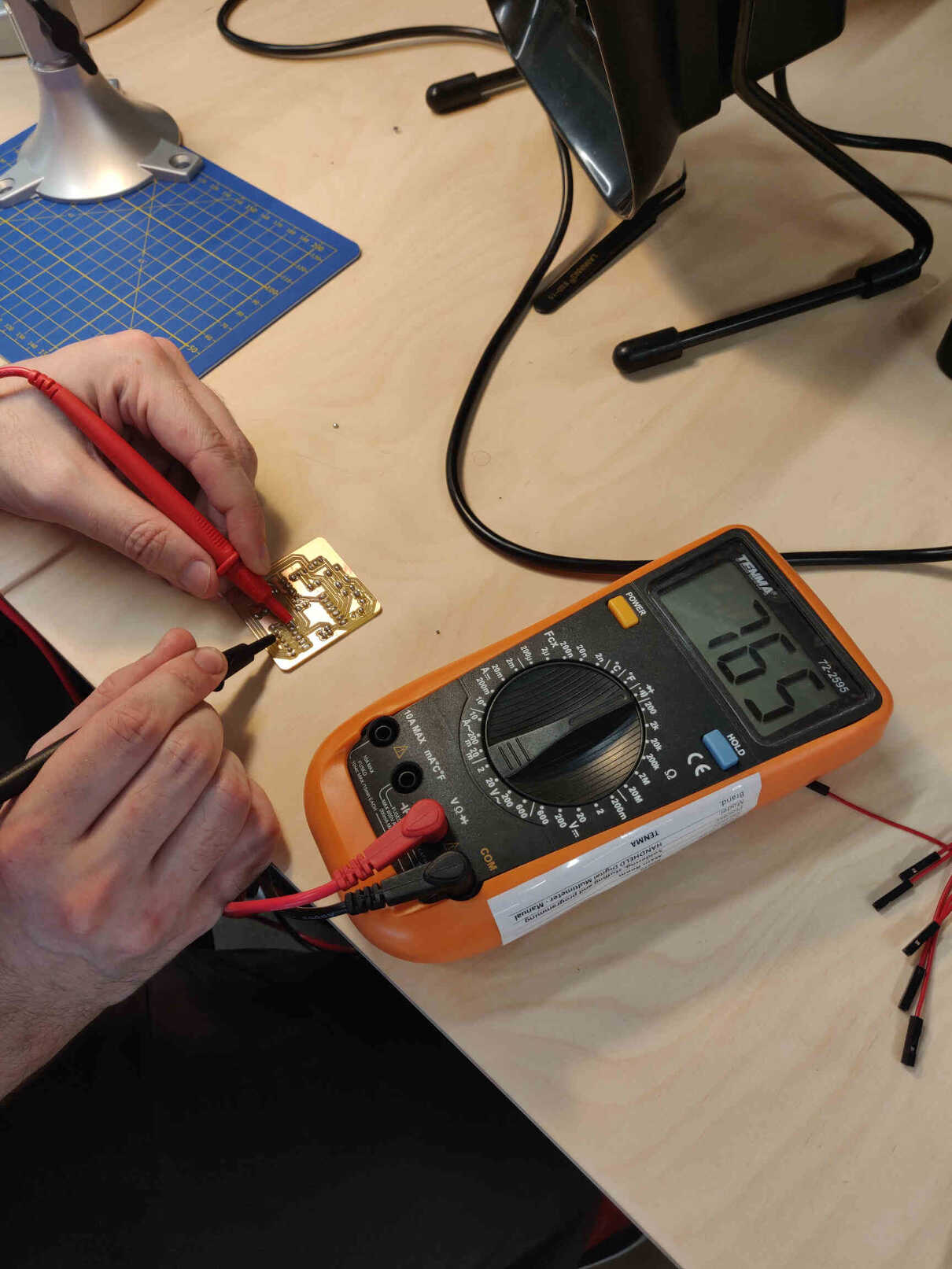
Testing the Quentorres
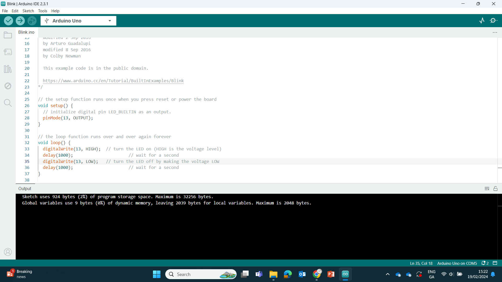
All that was left to do now was program my PCB to perform the Blink test. (Needs finishing).->
To see if my PCB is functional and able for programming, I downloaded Arduino IDE on the Fablab laptop and agreed to trust installations. Once inside the Arduino IDE, I went to Tools -> Boards -> Board Manager. Typed RP2040 and installed the board labelled “Raspberry Pi Pico/RP2040” and agreed to installation. Then I went back to Tools -> Boards -> Then selected ‘Raspberri Pico/2040 -> Then ‘Seeed XIAO RP 2040’.
After this I went to Tools -> Port -> Selected COM3. The tutorial I followed said a port labelled ‘COM5(Seeed XIAO RP2040)’ would appear but I didn’t get the option. Though after some small research COM3 is what we are also looking for.
That being said, my selection of COM3 changed itself to COM4 shortly after.
When following this tutorial and performing the Blink test example, the tutorial documented that Pin 25 would blink once per second upon upload. Although there was certainly a light blinking on the Seeed XIAO board, I couldn’t really tell if it was because of me or if it was just lighting up for another reason - such as a connection fault.
To test this, I changed the Arduino IDE delay code from 1000 -> 200. That way the light would blink every fifth of a second. After upload I can confirm the light blinking was from the Blink test - meaning the connection to my own manufactured board is successful!
Blink Test Code
void setup() {
// initialize digital pin LED_BUILTIN as an output.
pinMode(3, OUTPUT);
}
// the loop function runs over and over again forever
void loop() {
digitalWrite(3, HIGH); // turn the LED on (HIGH is the voltage level)
delay(200); // wait for a second
digitalWrite(3, LOW); // turn the LED off by making the voltage LOW
delay(200); // wait for a second
}
Blink Test Working Footage
Built-In LED Test
SMD LED Test
____________
Conclusion/Reflections
Electronics Production was something I was incredibly nervous about as I know nothing about electronics or designing PCBs. For the majority of the time doing research, I couldn’t follow / understand a word. I was constantly missing that ‘connection’ that would help me make sense of it all. I got great advice from Adrian and Rico during the Saturday Global Open Time where they strongly suggested that I stick to the basics, don’t overreach for extra credit or complicate things for myself. Just follow the tutorials step by step until it starts to make sense. So that’s exactly what I did.
I was taken through Arduino Basics with my instructor where we performed the Blink test using an Arduino and Breadboard. I still don’t understand how practicing on a breadboard makes the PCB design process easier to understand as the breadboard just seems like an unnecessary step to me that overcomplicates the steps I needed to take - though I know it’s helpful/vital to many others in understanding the connections.
Modsproject.org was an interesting tool. Initially I felt confused as I didn’t understand what it was or why it exists. But after going through the milling process several times, the site feels second-nature to me. It’s an incredibly resourceful tool that gives a good basis for setting up and converting your PCB designs into readable material for the milling machine. Though some tweaks to the values are still required.
I added my ‘Little Buddy’ logo that I designed for Week 3 Vinyl cutting to my Quentorres PCB using Inkscape and was happy with the results.
VPanel was very fun to use. There’s a bit of excitement in the air that I could break the End Mill or Copper plating by going a step too far. But it was really satisfying having control of the milling tool and easy to understand (after a few mistakes).
Milling was initially frustrating as I was on a strict time limit in the fablab (10 hours per week) and the milling tool was constantly having issues following the toolpath and taking FOREVER to do so. This ended up being issues relating to Zeroing the Z-axis properly, cutting speeds too low and creases in the tape holding down the copper plate. Once those issues were resolved, VPanel & the milling process were very easy to follow. Though there was still research to be done on making the trace lines thicker.
After my PCB was milled, I moved on to soldering the components to the Quentorres. Soldering was oddly relaxing despite how intense it can get. I really enjoy it! Initially there were issues with faulty equipment as detailed earlier but once that was sorted, I really enjoyed soldering the PCB. I then used the Multimeter to test the connections 0 leading to passable results. The connections were definitely there, just not that strong.
Then to round the assignment up, I tested PCB using Arduino IDE with Raspberri Pi libraries to perform several basic blink tests. Only 1 out of 3 LED’s worked. I wasn’t able to deduce and resolve the issue here until Week 8 as we had to move on to the next assignment. The little time I had access to the fablab was a definite issue here and it was quickly brought up to my instructors - who later went about securing me a key for nights where I needed to stay longer.
____________