8. Electronics Design
This week we discussed electronics design. I was excited to dive into the topic because although I have a vague recollection of some theoretical concepts of circuits from a couple of classes in college and have attempted to work with arduino dev boards 1-2 times since I graduated, I never really got past making some LEDs blink. My background did prove helpful in recognizing some high level ideas, but I've always wanted to know how electronics are actually designed, how specific components are decided on, and how their values are calculated. The intuition behind these things has always been mysterious yet extremely powerful. Although I still don't really know much about this alchemy, I do feel this week has helped me peer through the looking glass and gain the smallest bit of insight into how it's done.
Onto the task of the week
- Use an EDA tool to design a development board to interact and communicate with an embedded microcontroller
- Group assignment here
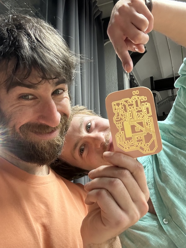
My board idea
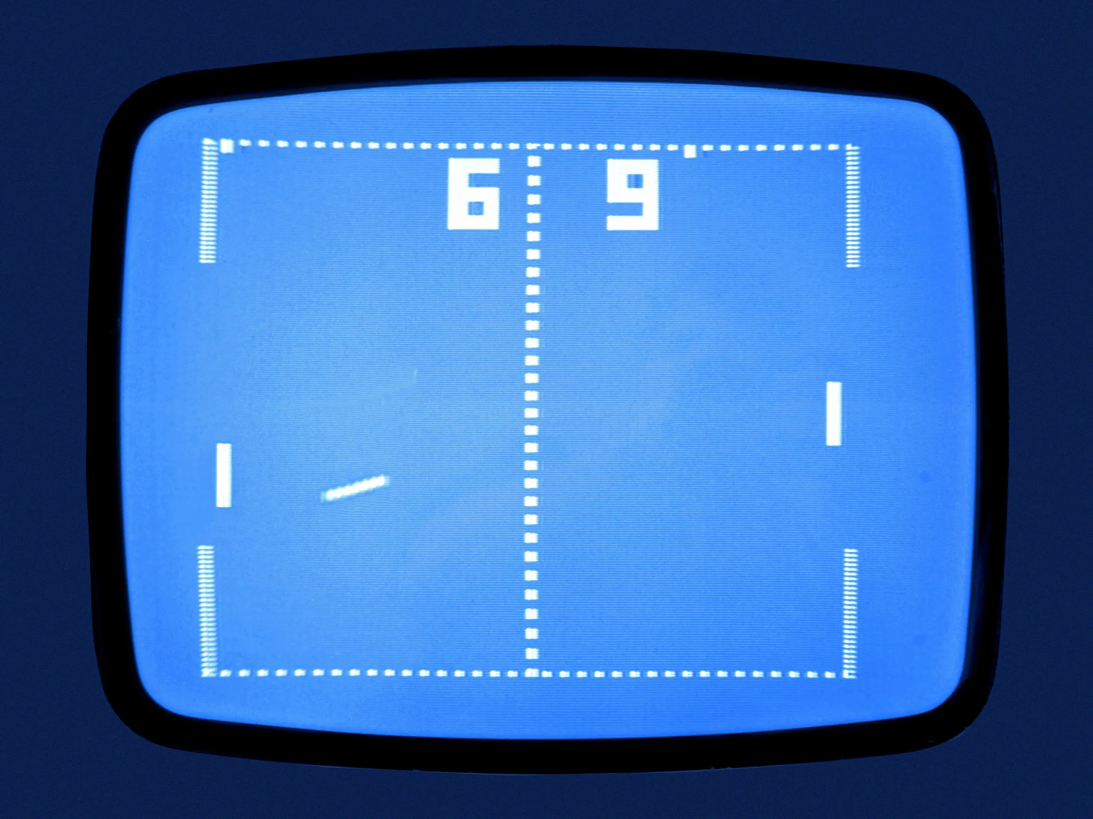
My goal was to create a portable (programmable) game console. This includes both
- a hardware aspect (the board design and controls)
- A really simple 2D game engine so users could make their own games (like pong, but perhaps worse).
- And a long ways off- make available IO headers so developers could bring their own controls into their games (this is definitely not in the short term)
All Hail King Kicad
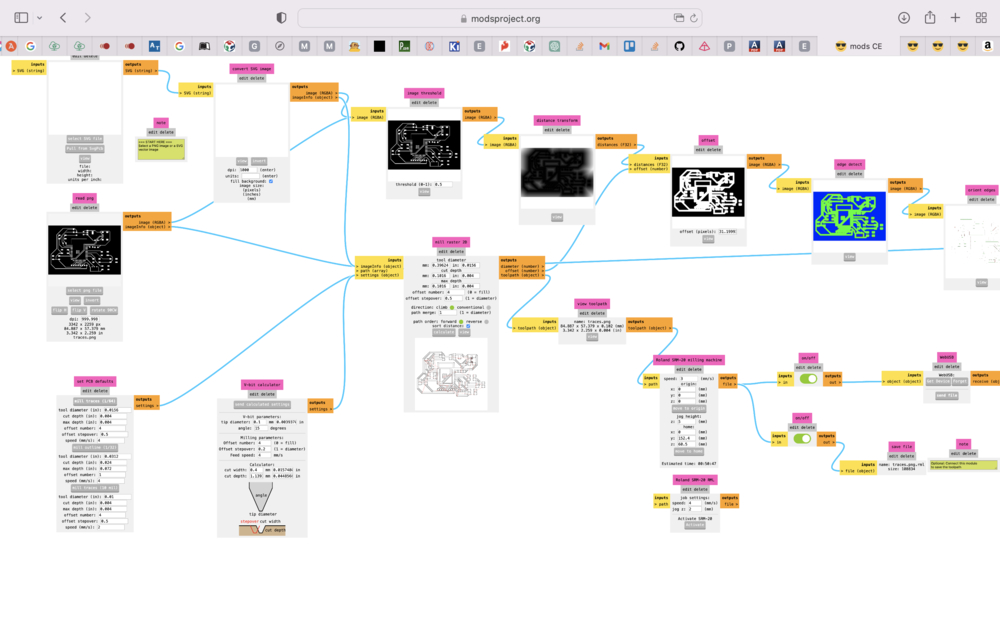
To develop our schematics and PCB designs we used a tool called Kicad. It offers a whole array of component libraries that you can use while in your design process and allows you to add more from other sources as well. We began by adding the electronic components available at the fab labs. Those footprints and symbols can be found here!
I would say our PCB design process can be broken into 3-4 major parts. Lets get into it.
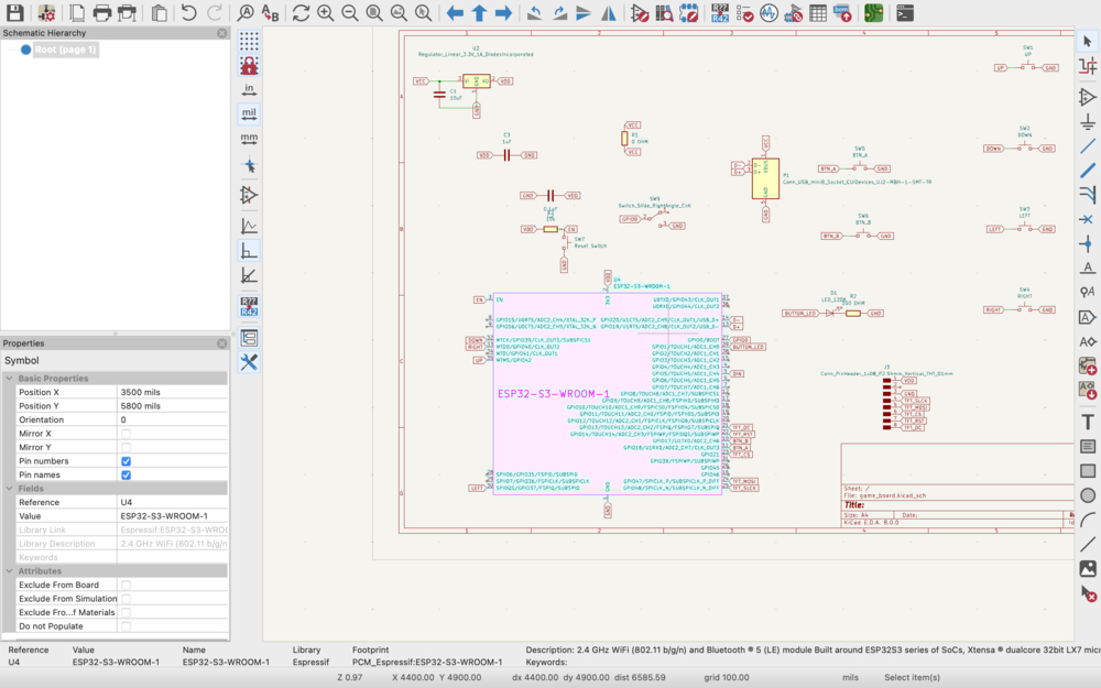
Schematic Design
First things first, we get started designing our schematic. The schematic is where we make logical connections between components we will use. This is done before we actually consider where those components will go in relation to each other. I felt this was very useful because you could gain a strong idea of how the circuit would be interconnected and function without worrying about the physical details of where each component goes and the wiring between them, which is a real puzzle in itself.
Shortcut keys in kicad's schematic design were also very useful.
- "a"- this brought up the components available from the library[ies] you're working with. In this case we limited ourselves to the fab academy compoent library to assure whatever parts we selected would be available (more or less!!).
- cmd+L- Bring up labels. Labels are very useful in connecting different components without the need of running wire between each of them. This keeps your schematic fresh n clean.
PCB Design
This is where you start to see your ideas actually take shape and see what it'll actually look like IRL. Be not deceived though, getting the wiring and pieces aligned all without any unintended connections is no joke. I definitely found myself lost many times in the PCB abyss which did lead me to rethink and simplify my design. Placing your voltage/power supply strategically is a good first step in keeping things open and organized for your board. Put it in the wrong place and you'll have a VCC line more insurmountable than the northern wall in Game of Thrones

I had a lot of switches for the gaming buttons and all of them had VCC connections. After an initial design an idea sprang into my head to actually make them connected to ground and take advantage of ESP32s internal pull-up resistors, which would set the pins high until a button was pushed and receive a low signal. This meant my yes's were nos and nos were yes's which can be a bit confusing but the nice thing is I avoided wrapping my VCC line around my board to get to my numerous buttons. Kul. Finally I exported my circuit design as a black and white SVG file.
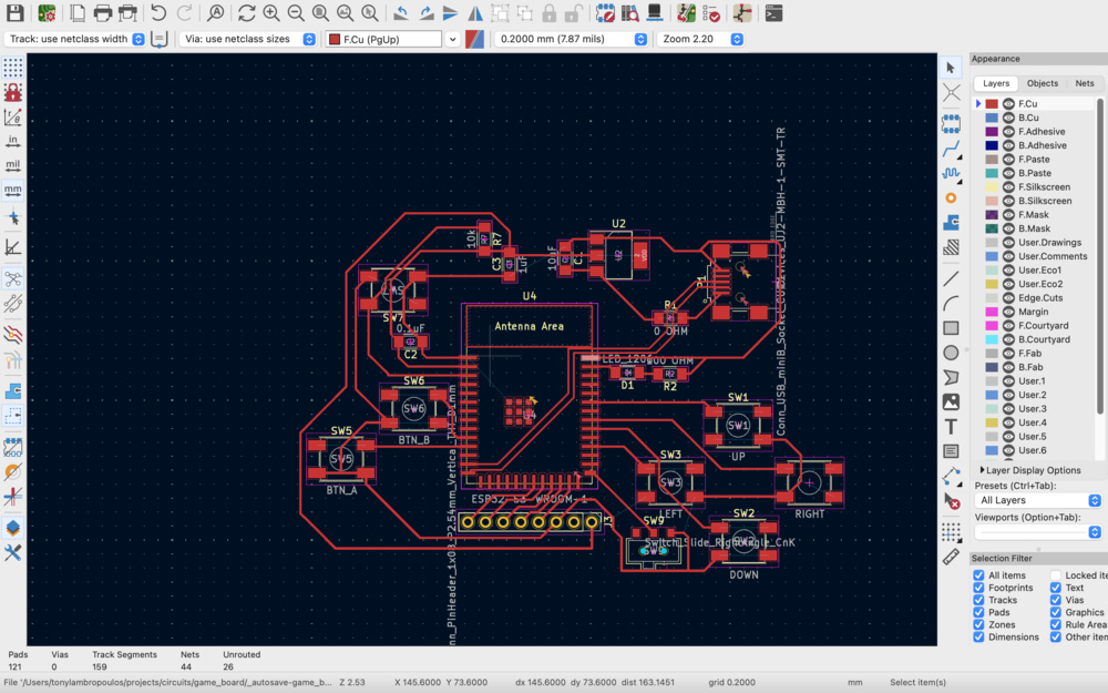


- "x"- this would activate the wiring tool.
- clicking on a component and then pressing "d". This was useful when a component is connected and you want to maintain its connections but move it elsewhere.
- "e" to edit properties like wire width and pad size. Can also mass copy properties to other components which is nice.
Ink[I wish I could e]scape
In week 4 we were given the PNGs all set to work with the milling software for the Quentorres board and didn't have to worry about this step much. But this week we had to actually do this ourselves. Here are some post-processing steps we had to do. In this case I used Inkscape to do them but it can be done with any image editor (like illustrator or probably kicad itself)
- Invert the colors of the SVG output from kicad- Kicad outputs a circuit where the background is white and the wiring is black. The milling software we use expects the opposite. Basically anywhere white on the image it leaves unmilled. Anywhere black is removed
- Breaking the SVG into multiple layers. When milling you will want the process broken into steps. Our 3 general steps are milling the traces, then cutting the holes, followed by cutting out the board. My limited ability on Inkscape made this step very frustrating. But with some help from an instructor, I found a consistent workflow. Some key points were
- Filters->colors->invert. This changes black to white and vice versa in Inkscape.
- Find the holes and move them to another layer (this step could use improving)
- Make a white and a black backgorund of identical size. One is used to drill holes and the other is used the trace
- Exporting the different layers to PNGs
Trace PNG 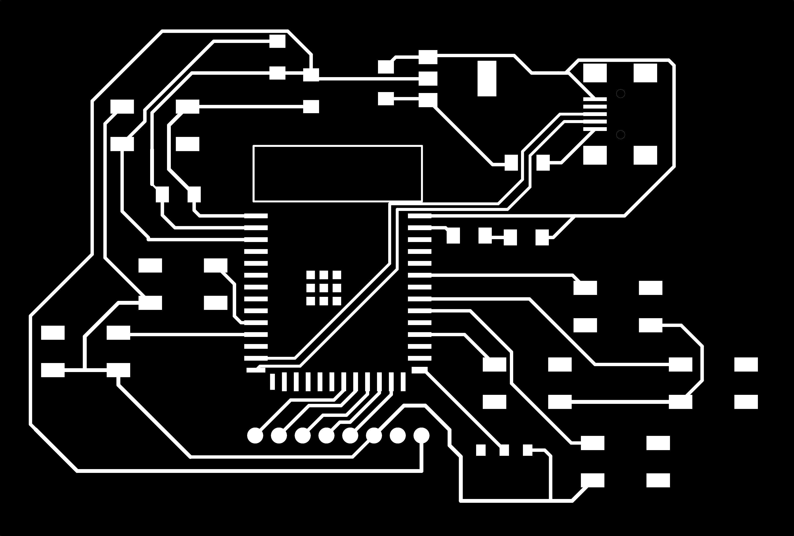
holes PNG 
Outline PNG 
Mods Mods Mods
This was already covered in week 04. We used the website once again to create the milling files. This time though after cutting the board I noticed the esp32 needs a copperless space right above it so its antenna can work properly. I would potentially have to manually remove that with a cutting knife. That didnt sound fun. I ended up preparing one more PNG and subsequent milling job where I used the 1/32 inch mill to remove the block of copper in this space.

That definitely saved me a lot of future time and effort. Finally I outputted the files for the mill to read and put them on the iaac cloud filesystem.
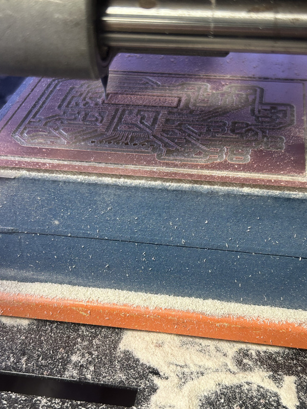
Mill Baby Mill
Finally, let's get physical. I milled my first board and all looked well.
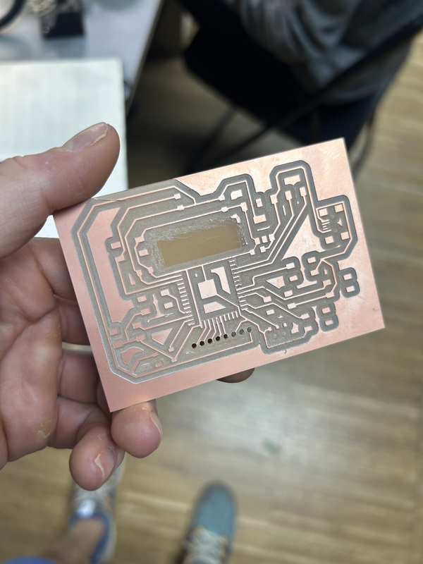
I still had to scratch off some copper for the antenna because I wasn't super precise on where it was on the first go. I also accidentally drilled out the copper around the holes by accident. This must've happened when I went into the heart of darkess that is Inkscape the first time. Along with being a double sided copper board, this wasn't an ideal situation. My board was primed for short circuiting. I decided to reprint, this time with a one sided copper board, better holes and better antenna space coverage.
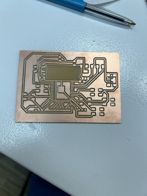
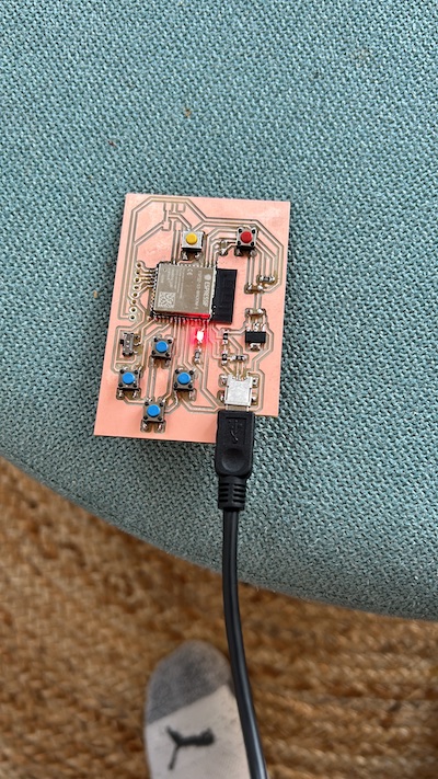
I was really pleased with how my second board turned out! Everything was improved. Now that I had my milled board I would be able to start adding my components to it, starting with the microcontro....but darn we don't have the ESP32 model I chose to use...I had to go back and rewire everything with one we did actually have in stock. I also had to import the symbols and footprints here (for the s3-wroom-1). That was definitely sad times. Now I would reprint for the 3rd time
After several failures and a rewiring required I was left a bit demoralized by the day. I knew I had to do somethng about it. I stuffed myself silly that night to fill the void

Things learned
- Finding a consistent workflow is very important. There are many many places for the process to go wrong and the more you can minizize variance, the better.
- Even if in theory there is inventory of a particular component or chip, you should always check!
- How to use datasheets to consider power requirements for different components and how to do the calculations to add resistors when required. They look daunting but are very useful.
- Capacitors are very useful for stabilizing voltage across components on the circuit. They are like tiny storage units for electricity within electronic devices, holding a charge temporarily and then releasing it when needed. Think of them as small batteries that can charge and discharge very quickly.
- Being thoughtful about how your ground (GND) and power (VCC/VDD) lines get routed on your PCBS, because they will touch almost everything
- The merit of a multi-layered PCB. We only used one layer for this week's task and I could see already how having multiple layers would really free up a lot of design constraints.
- Wire thickness is an important consideration. At our voltages and currents it wasn't especially important but thin wiring can have a signficant impact on the circuit and be a limiting factor.
- The function of pull-up/down resistors- basically forcing a 0 or a 1 on an input pin. This is important to keep things predictable. Read more about that here
- When working with an IO pin on a micro controller always ask yourself if a pull-up or pull-down resistor is required
- Diodes are very useful and serve many processes. Some are...
- Blocks or diverts excess voltage to protect electronic components.
- Helps convert alternating current (AC) to direct current (DC) for charging devices.
Kicad Files
Kicad files can be found here