WEEK 8 / Electronics Design
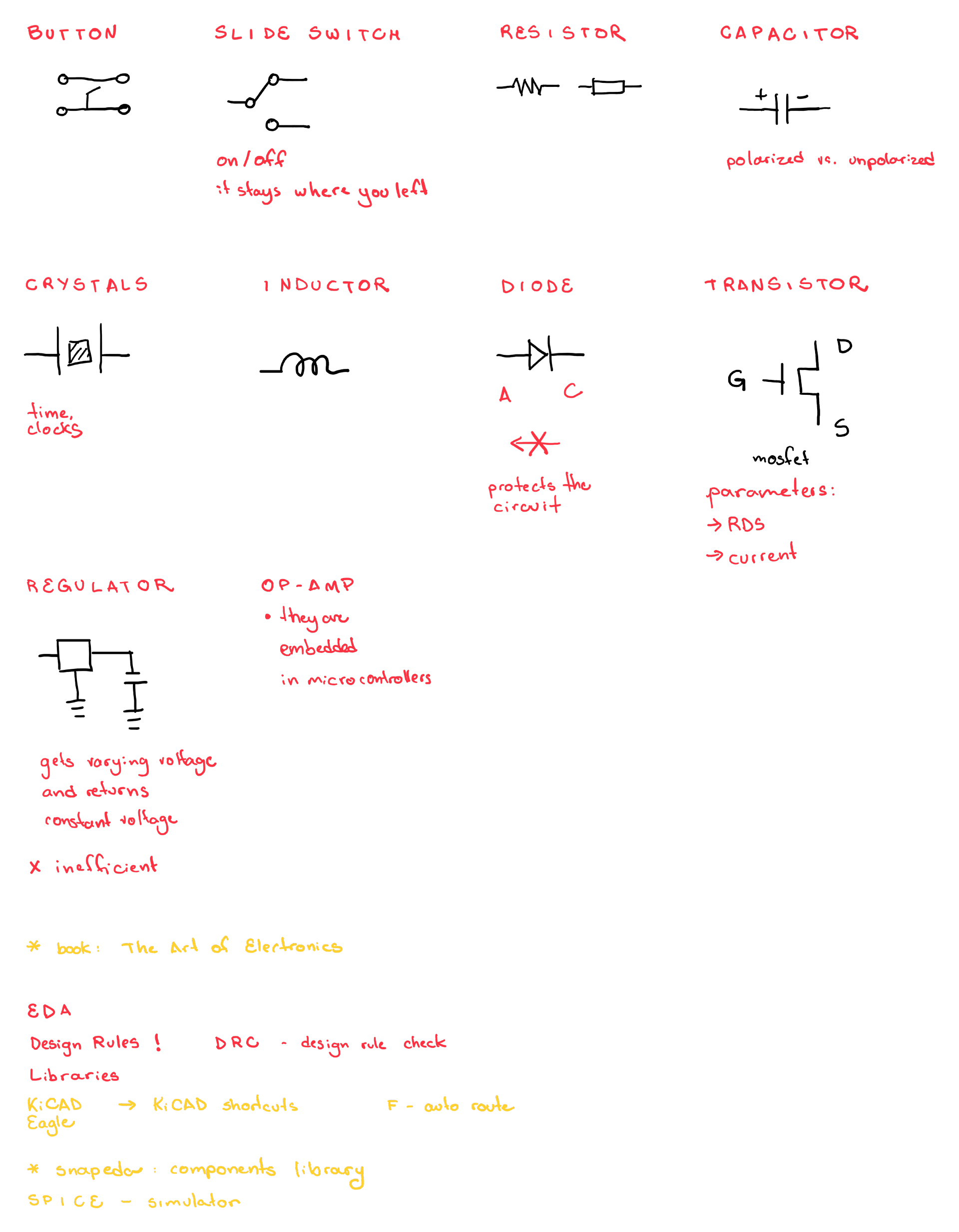
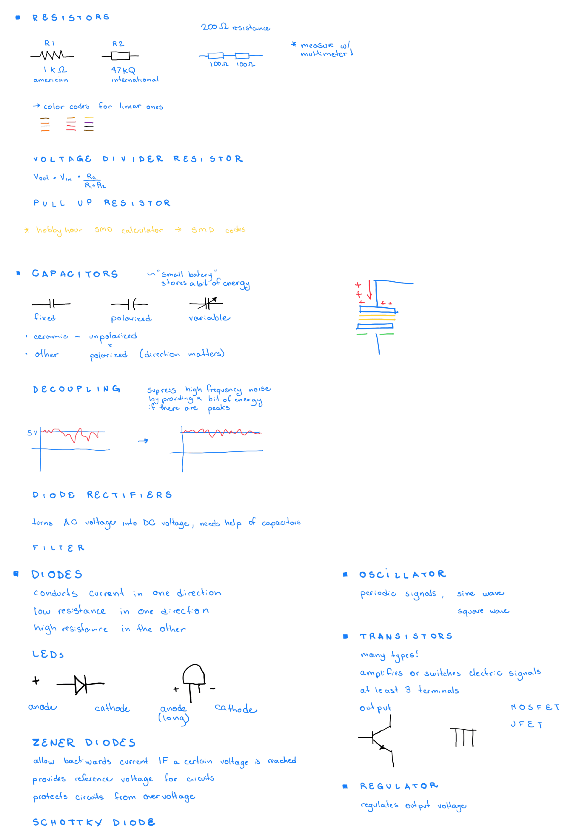
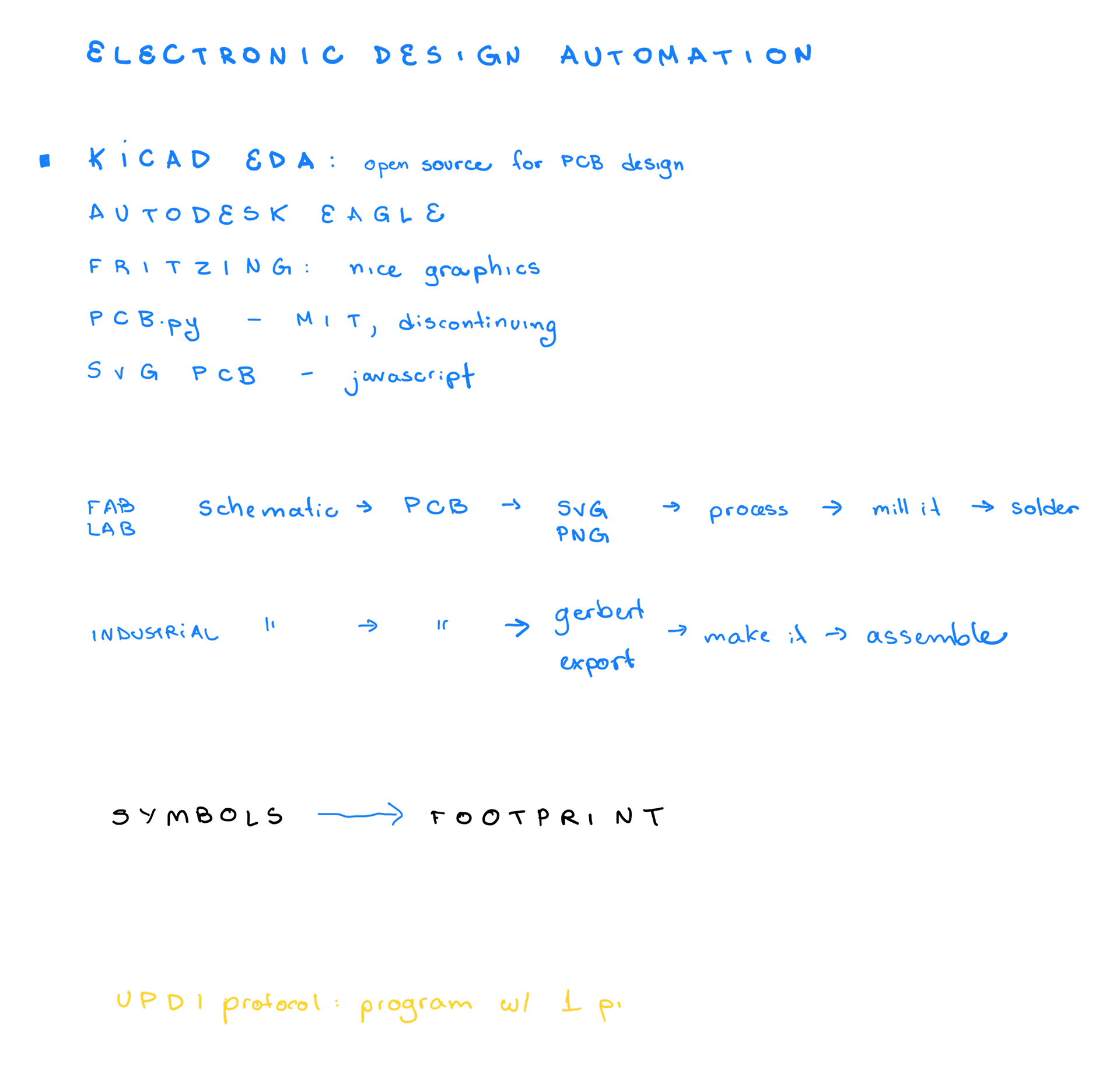
This week we started learning how to design electronics.
Weekly assignments
Group assignment
Use the test equipment in your lab to observe the operation of a microcontroller circuit board (as a minimum, you should demonstrate the use of a multimeter and oscilloscope).
You can find the group assignment in our group page.
Individual assignment
Use an EDA tool to design a development board to interact and communicate with an embedded microcontroller, produce it, and test it.
First attempt - ATtiny1620 board
For this week's assigment I had to first find out what a development board was and what was a board that was a non-development one.
I learned that the development board is used to program other boards. I spent the initial part of the week doing research on microcontrollers and components. I learned that the microcontroller of the development board should have compatible architecture to the one it is programming. As the ATtiny series still seemed like an appropriate choice for my project, I decided to design an ATtiny1620 development board. even though I knew the development board didn't need to match the design of the PCB I would include in my pencil, I thought it would be a good opportunity to start the design exercise of working with the width constraints the pencil would require.
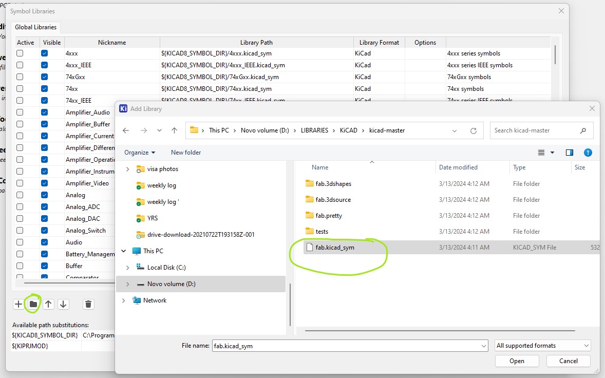
To design the PCB, I used KiCAD.
The first step, was to load the local components library of our fab lab, so we would design with the components we have (and turn off the visibility of the global libraries, to not get confused).
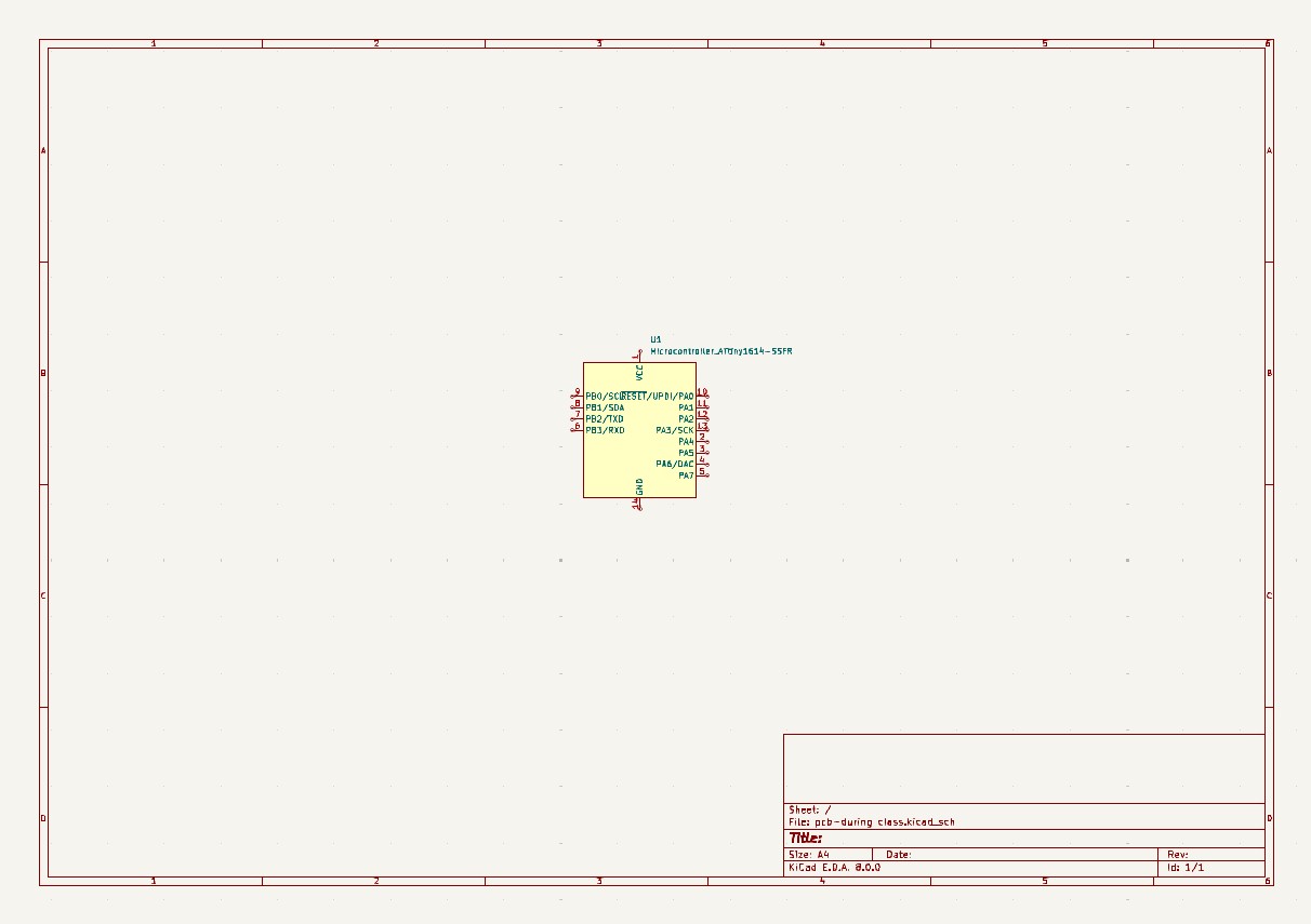
After creating a project, there is a schematic page and a board editing page. In the schematics there is shortcut "A" to add components.
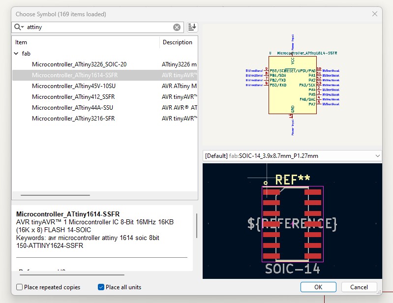
In the top riboon, there is a button to switch to the board editing page. There, you can load the footprints as components you placed in the schematic.
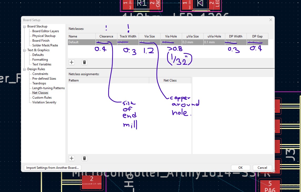
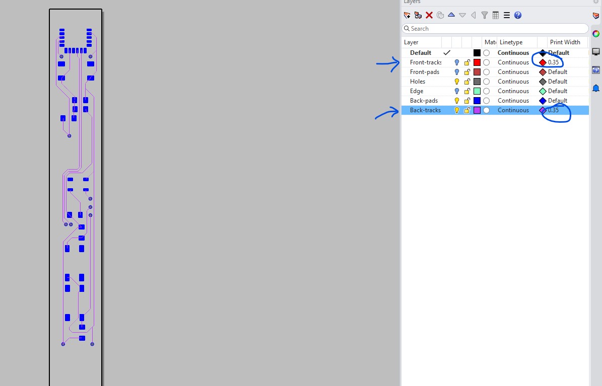
There are some important settings to always check. In track sizes, at the top left, there is an "edit pre-defined sizes" setting, in which we set the track sizes and limits according to our milling machine rules. Also made a note to avoid sharp corners when designing.

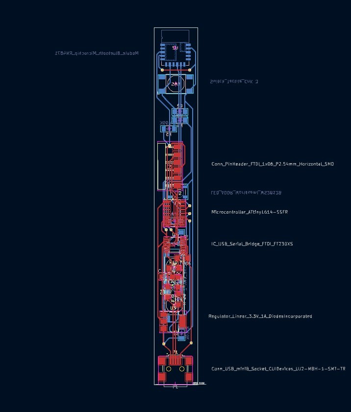
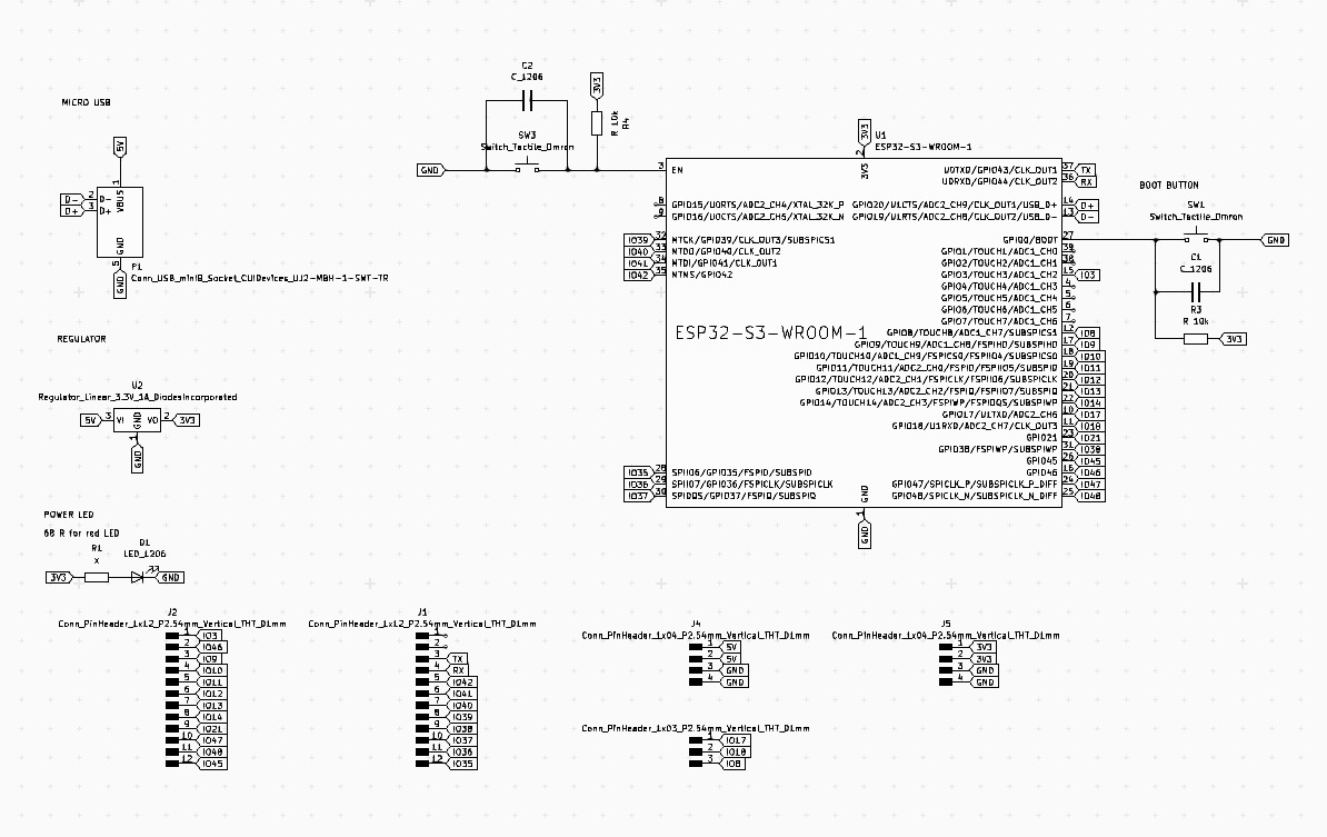
Back to the schematics, this was the result of my online research and talks to instructors and peers. Micro USB as it was the port available in the lab, a regulator for the serial-to-uart components (requires 3.3V instead of regular 5V from the USB). Then microcontroller, bluetooth, neopixel, and 3 buttons.
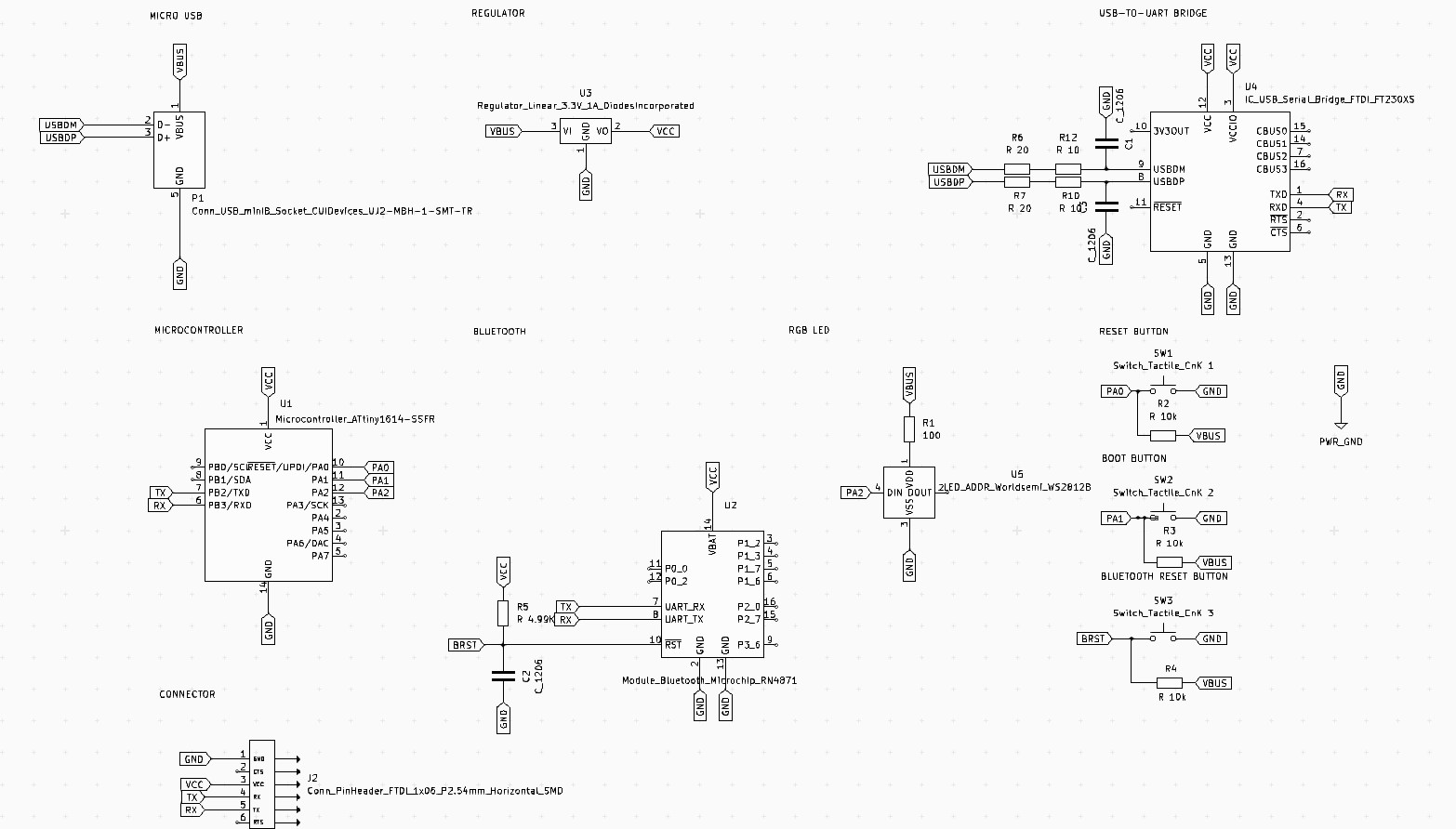
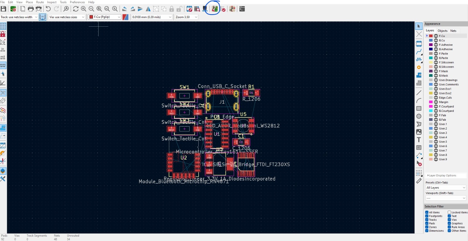
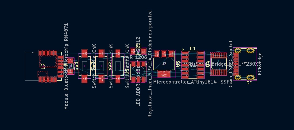
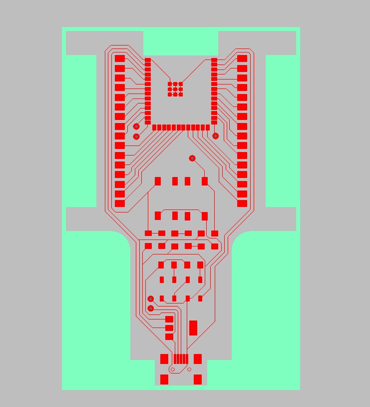
For the PCB, there was a lot of back and forth - placing the components in a linear matter gave a lot of trouble when tracing the routes.
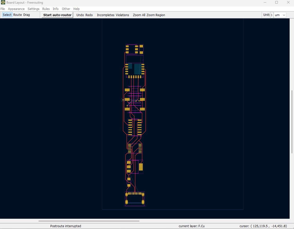
I also gave a try to the "Freerouting" plugin, which is really cool. When done placing the footprint in the PCB editor, you can export a specctra file and auto-route the PCB. My layout was resulting in PCBs with 2 layers. There is an option to not include vias, but it was resulting in infinite attempts as it would be impossible in the configurations I had.
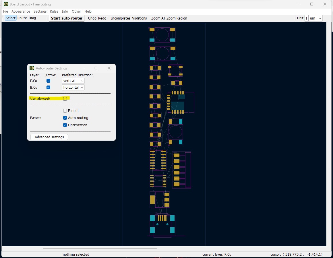
Since using 2 layers was the only way I could keep the linearity, I decided to manually design it (and maybe learn how to do it lol) and instead of placing just a few segments like the auto-router suggested, I decided to place half of components there. It would make the connections with the microcontroller much easier and it would be cool to learn. The design wasn't really good, there is a whole bunch of empty space in the front layer, which could have been more balanced - but I focused on getting everything connected and moving forward.
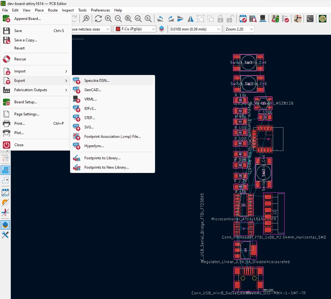
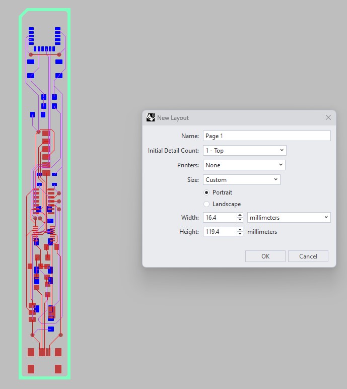
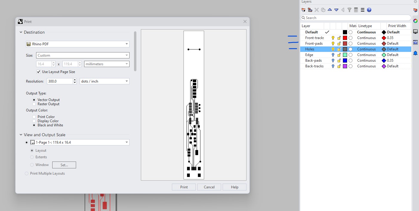
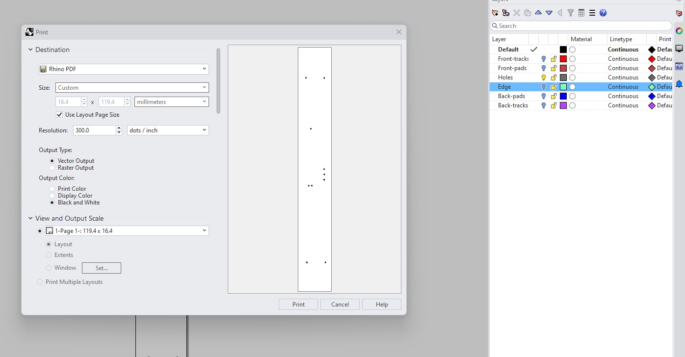
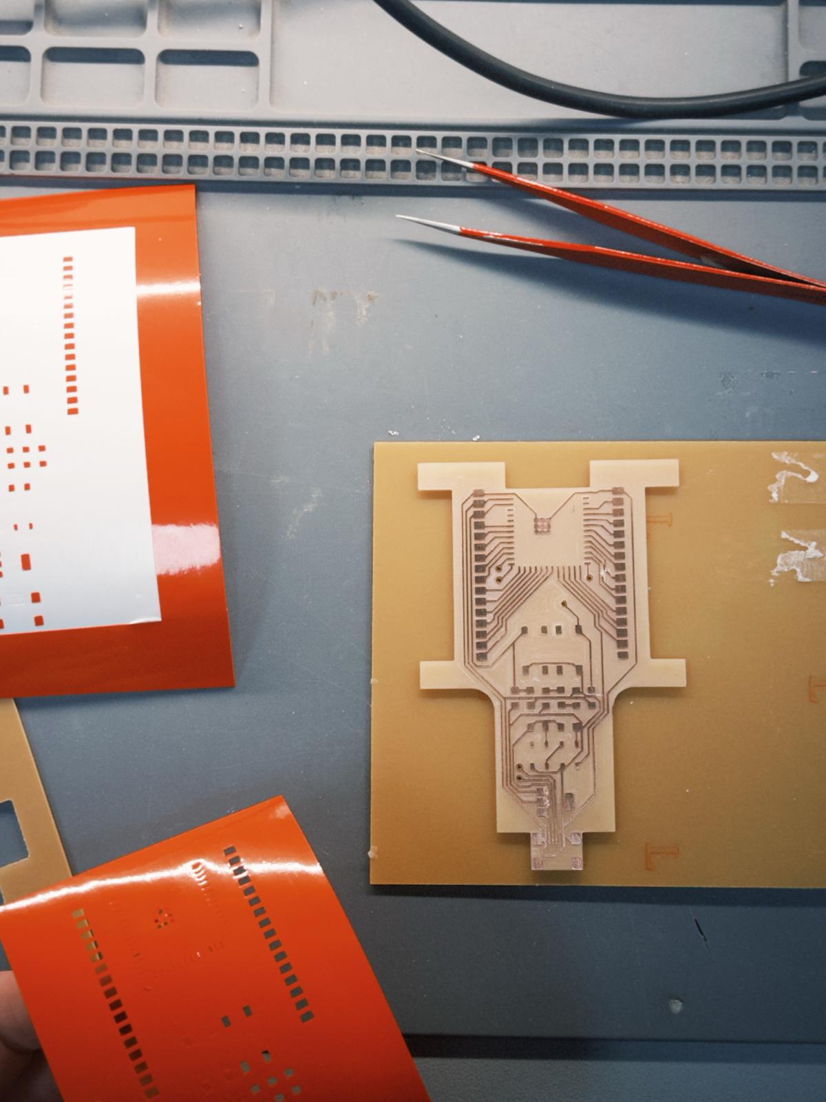
I exported the copper layers from front and back, as well as the vias, as an SVG file and imported them in Rhino, where I could edit the line widths and setup print options. I imported the files separately and set different layers for the different classes. Also set a Layout with the size of the PCB I wanted and drew the outline I wanted to cut. For the pads, holes and outlines, I created hatches. The tracks are lines with no weights, so on those layers I set line widths with the track sizes I wanted. Then printed PDFs
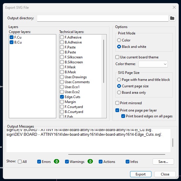
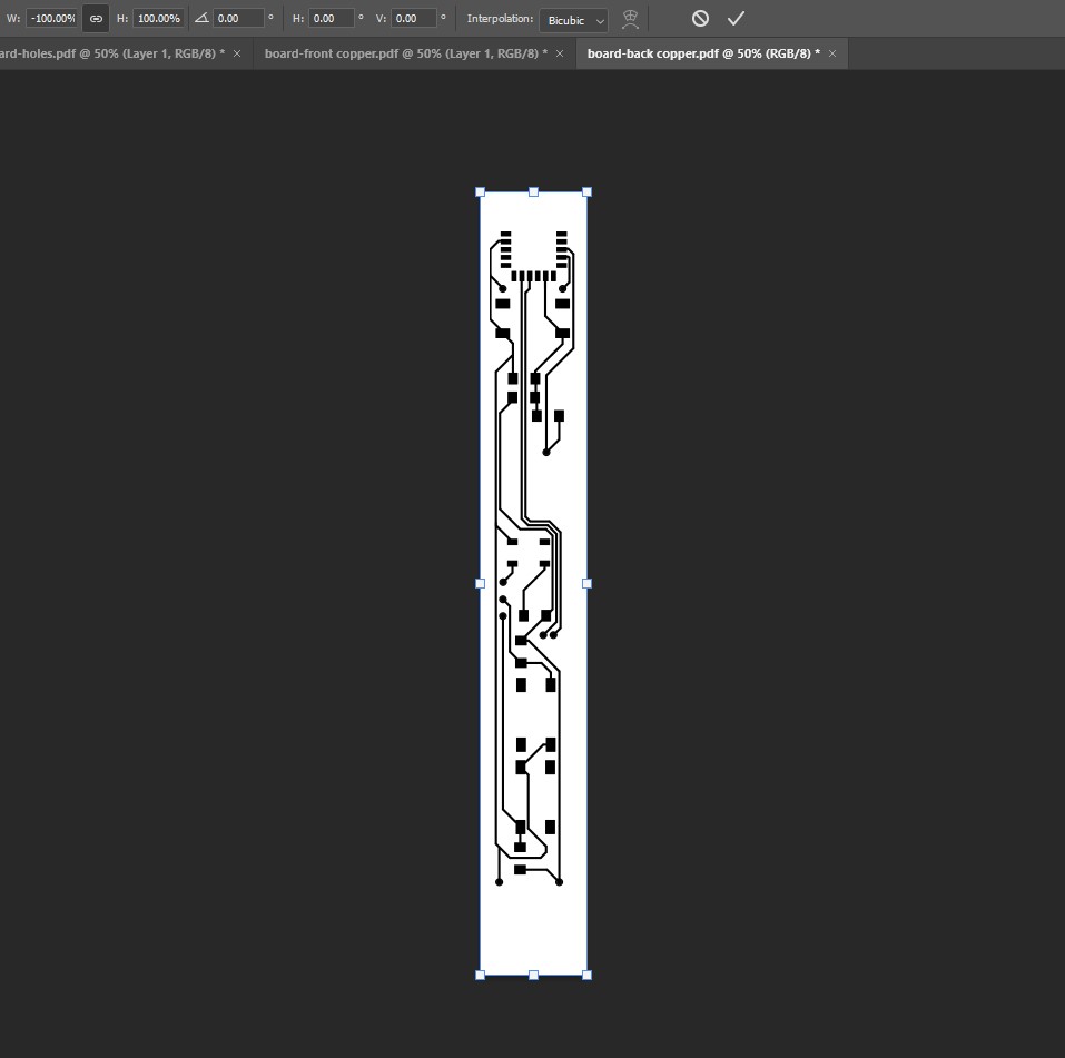
I then converted each PDF exported from rhino into PNGs in Photoshop. Then followed the steps of processing the PNGs in modsproject.org - steps explained in Week 4 page.
SPECIAL ATTENTION TO
Holes layer: initially, I had the diameter set to 0.8mm, which was close to the mill's size. When I later imported the PNG to mods, the calculation would only get one hole for some reason. Increasing the diameter of the holes to 0.81mm in Rhino solved it.
Back copper layer: When converting the PDF into PNG in Photoshop, I also mirrored this image file, since KiCAD doesn't do that (by default, I am not sure if there is a way to customize it).
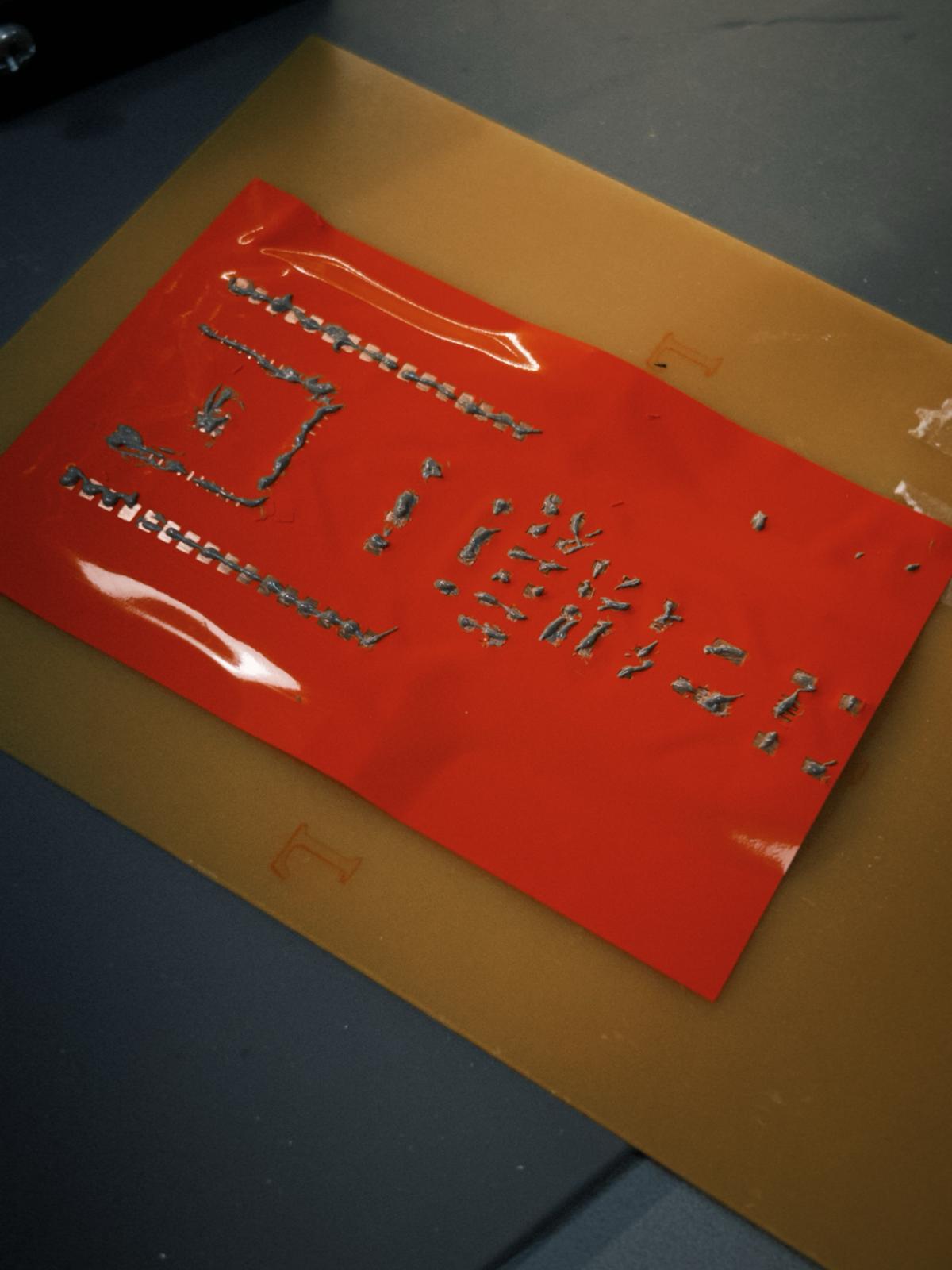
Then cutting was a bit of a disaster. The cut depths were too strong and I didn't manage to align top and bottom layers correctly. I used a marker. I will attempt a different approach next time.
the rest is still in progress, I'll come back with updates.
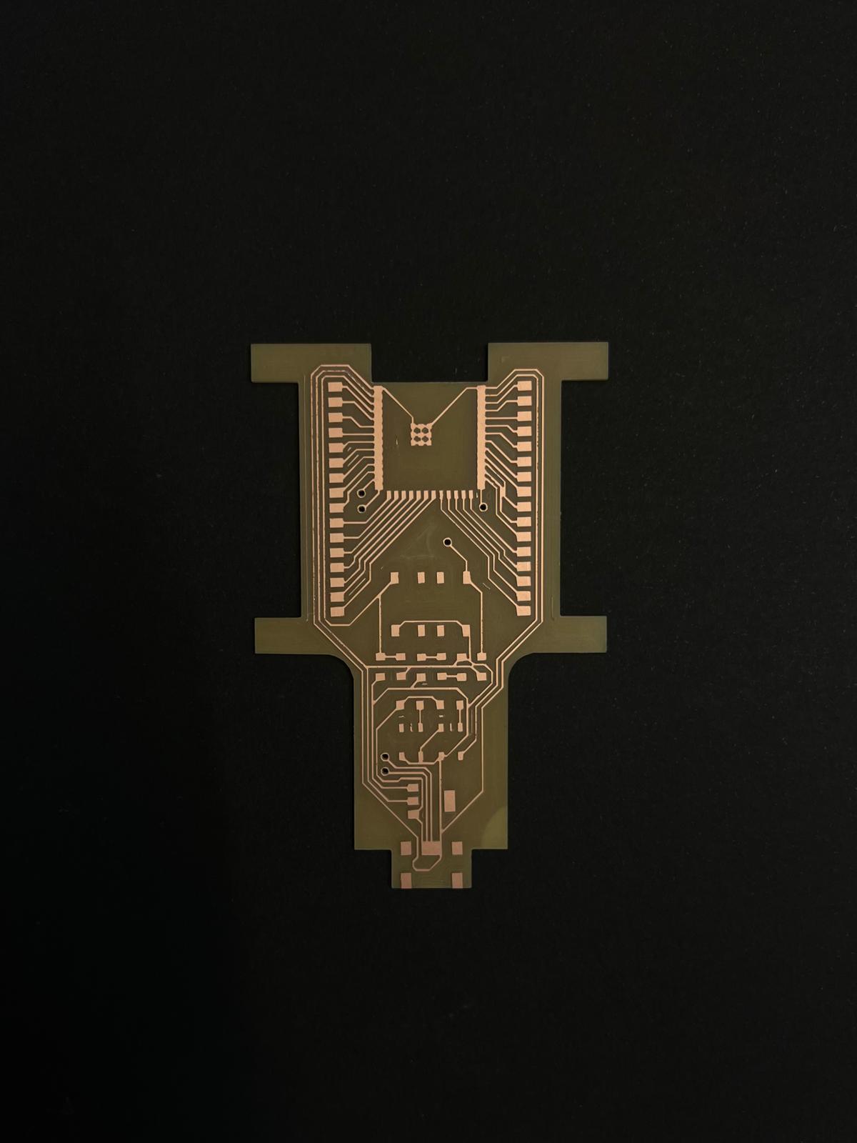
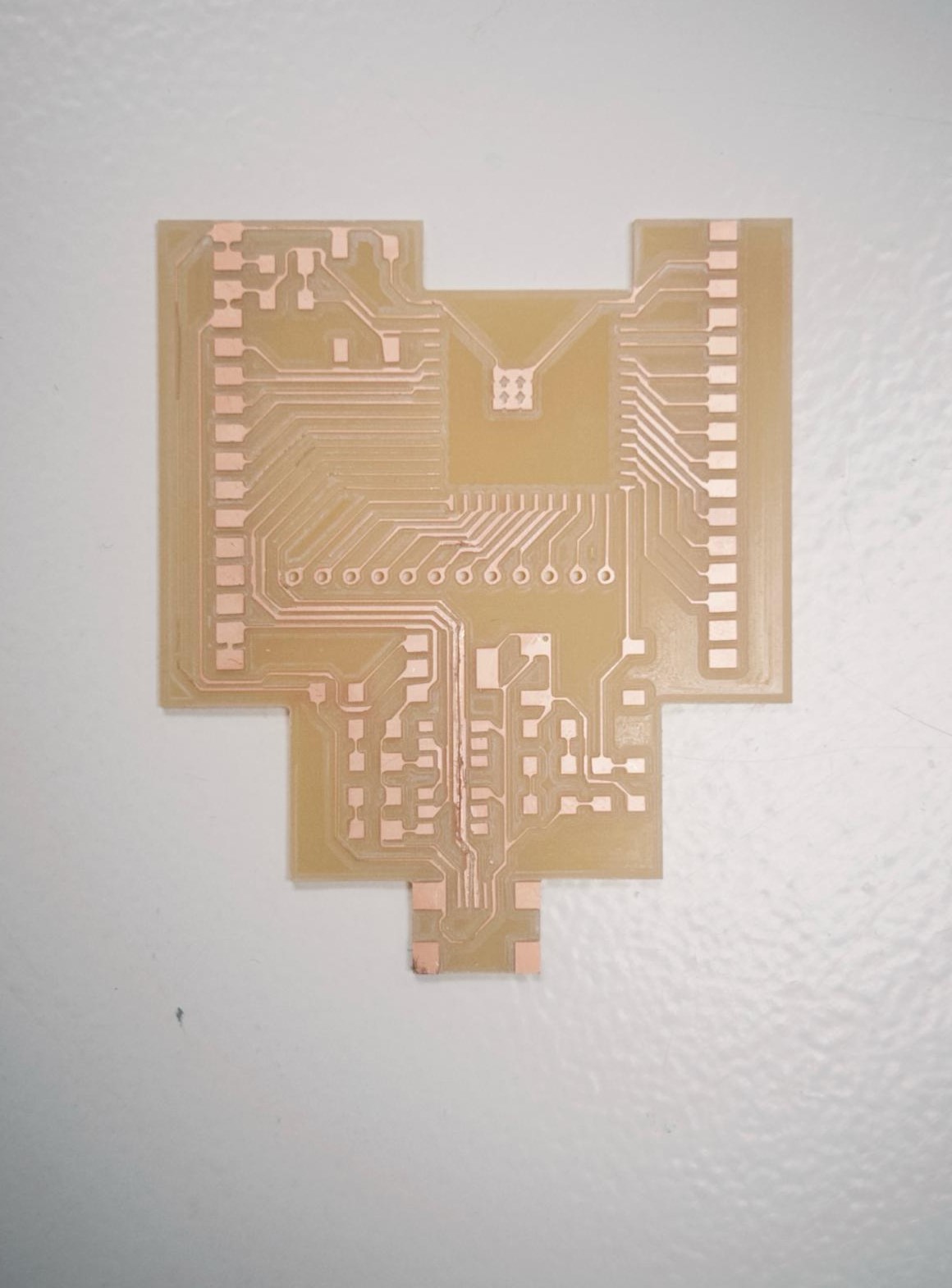
Second attempt - ESP32-S3-WROOM-W1 board
After discussions amongst my classmates regarding difficulties with the ATtiny, I started to get worried I would have a lot of trouble programming it, since I'm quite new to this. Also, it seemed like the board was getting overcomplicated with the separated bluetooth component. Everything was getting too complex with very unsure results. So I decided to switch my design to incorporate an ESP32, which would provide good processing capacity and wireless functionalities. Later, hopefully, I can figure out how to either work with the size of this microcontroller on my final project board, or test compatibilities with different architectures. A problem for myself in a few weeks.
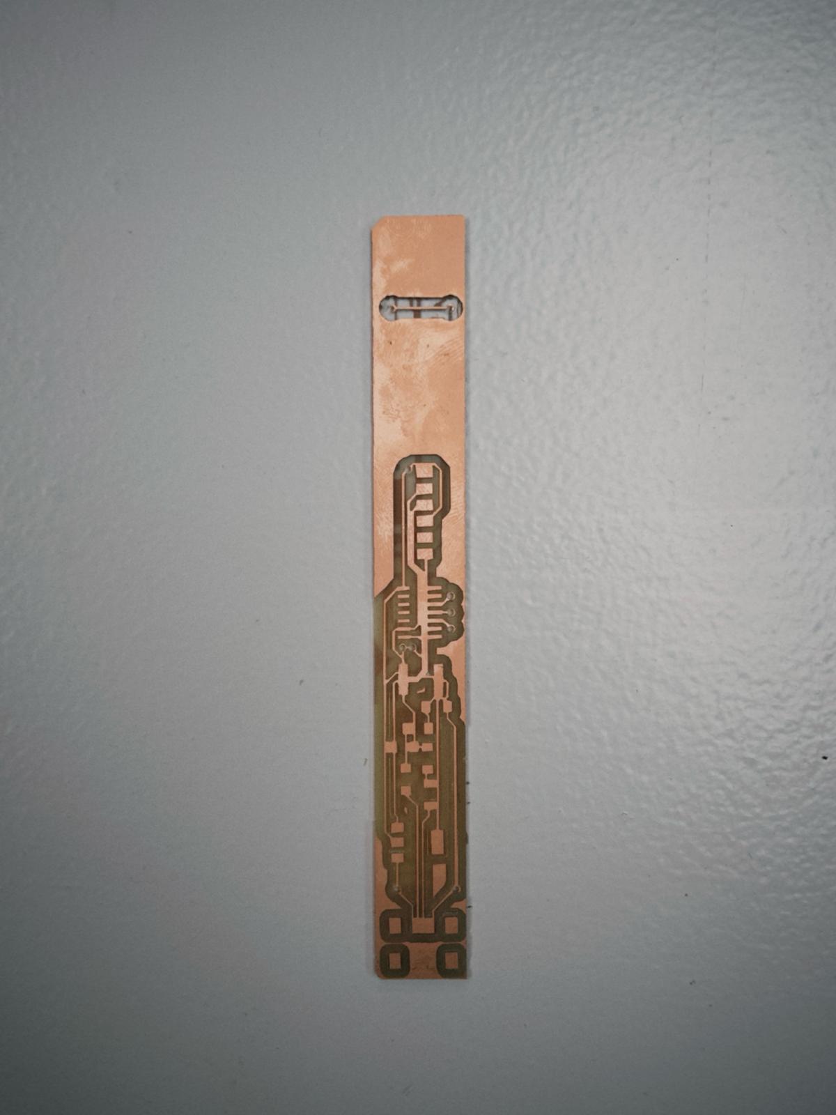
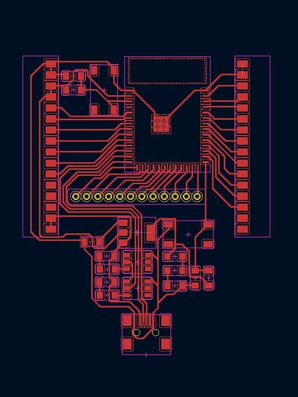
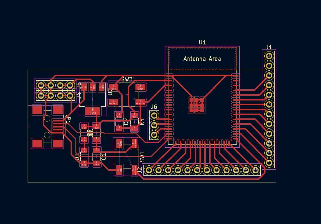
There were fewer components than the previous board, but a lot more pins. I wanted to make use of most of them, since I didn't know exactly which ones I would need to use. The schematic kept changing, a few adjustments here and there, but this was the overall plan.
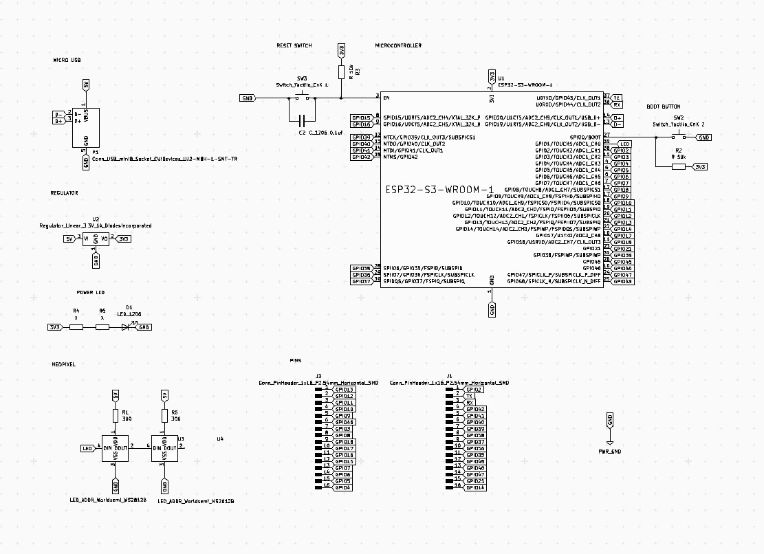
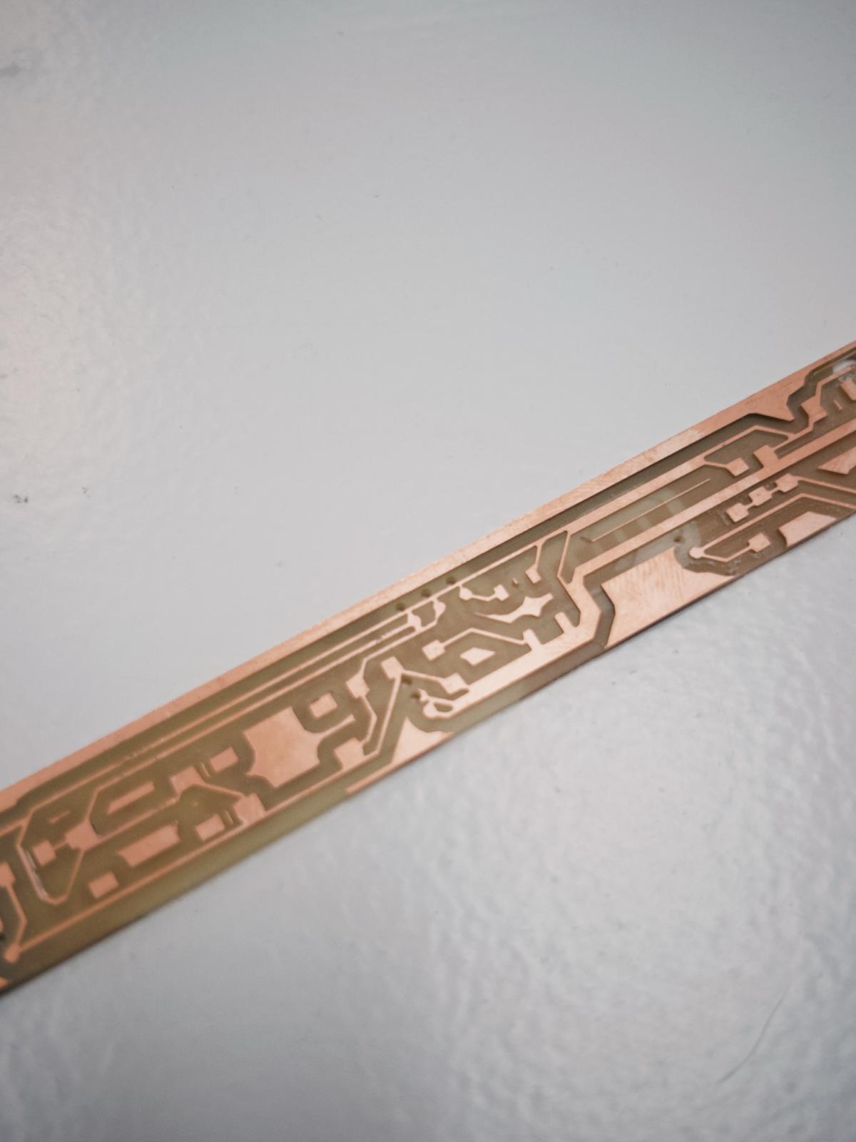
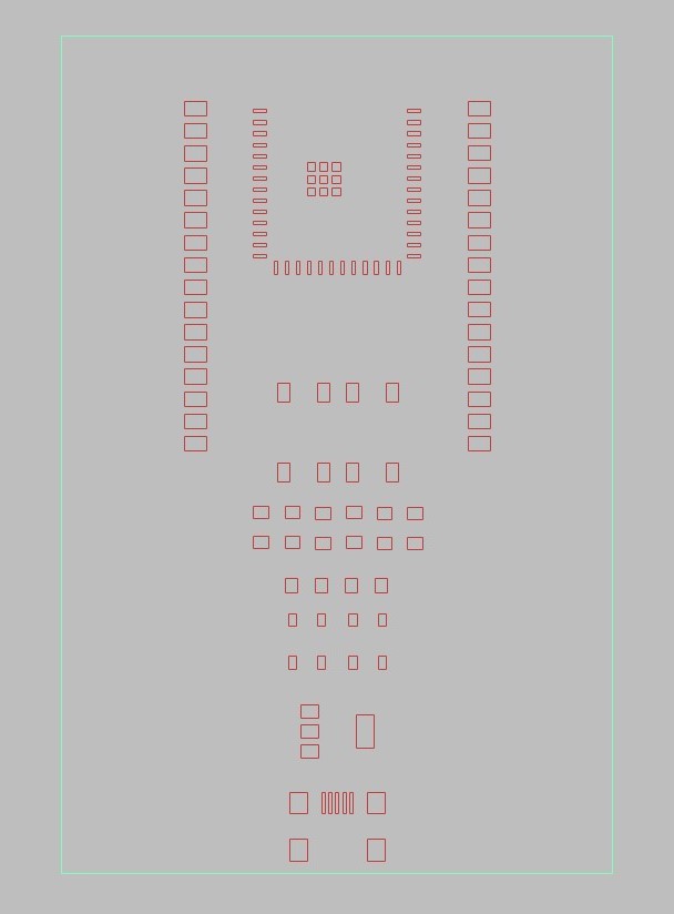
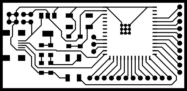
Designing the PCB was a long process. It seemed I wouldn't be able to get all the pins and all the connections I needed without vias. But for this one I decided to test wiring instead of cutting the back layer. After I milled it, I was pretty happy with the result! However some of the pads and tracks were connected. It took me another 2 rounds of adjusting them on KiCAD/Rhino, to get it properly.
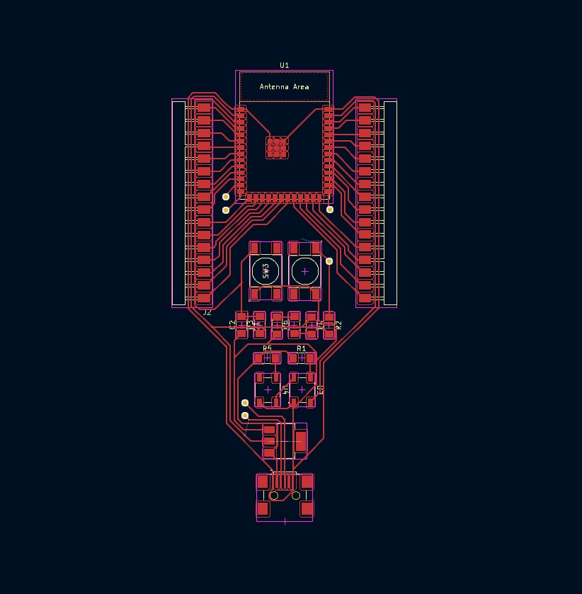
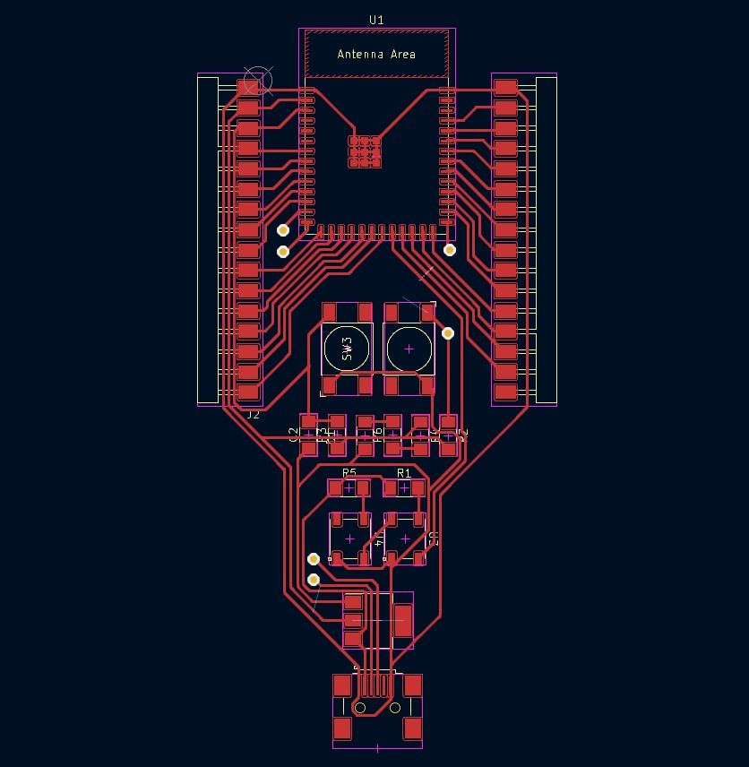
The best results I got was setting a 0.9mm offset between lines on Rhino, and line weight to 0.35mm.
Then to soldering the components. Since there were tiny component parts to be soldered, such as the USB and the microcontroller, I thought I'd like to test paste soldering.
It didn't solve all my problems as I was hoping! It worked to place the components and prevent them to move around, but I had to add a whole bunch of solder afterwards to all the pads regardless. Maybe if the stencil holes were larger and I had added more paste it would have resulted in a more permanent solution. Also added the additional brass lines on top to link my D+ and D- and my boot switch.
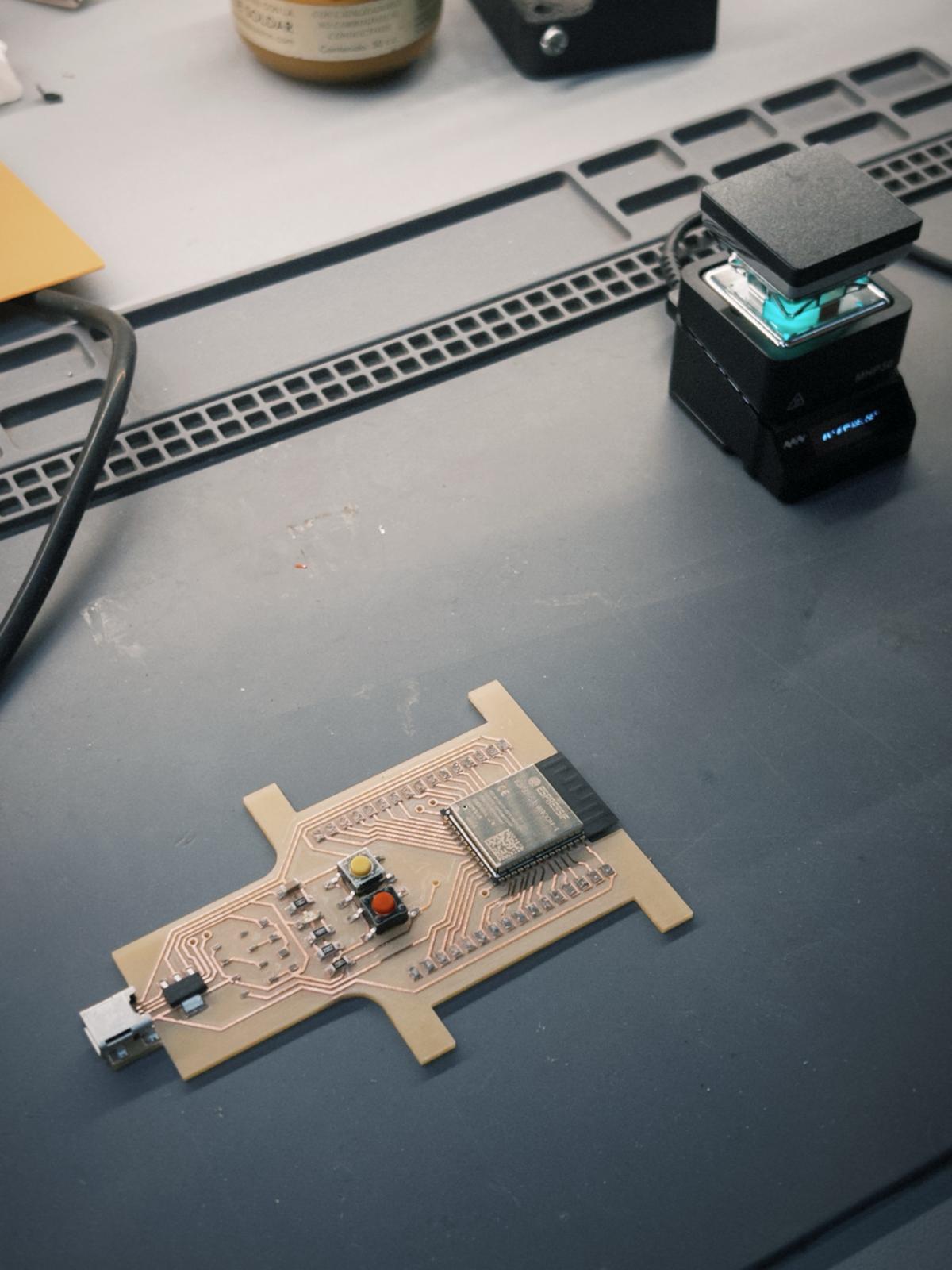
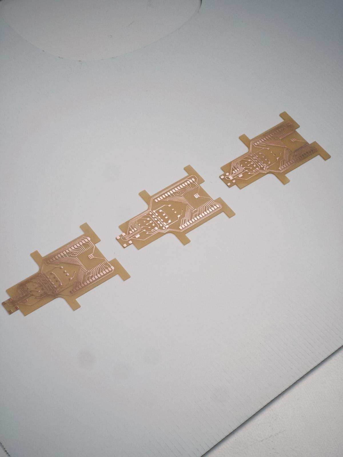
Even though the board turned out OK... It wouldn't light up the LED when connected to the USB. This was already Output Devices Friday. I would't be able to fabricate another board on the weekend, so thought maybe I should redesign it, just in case :'[
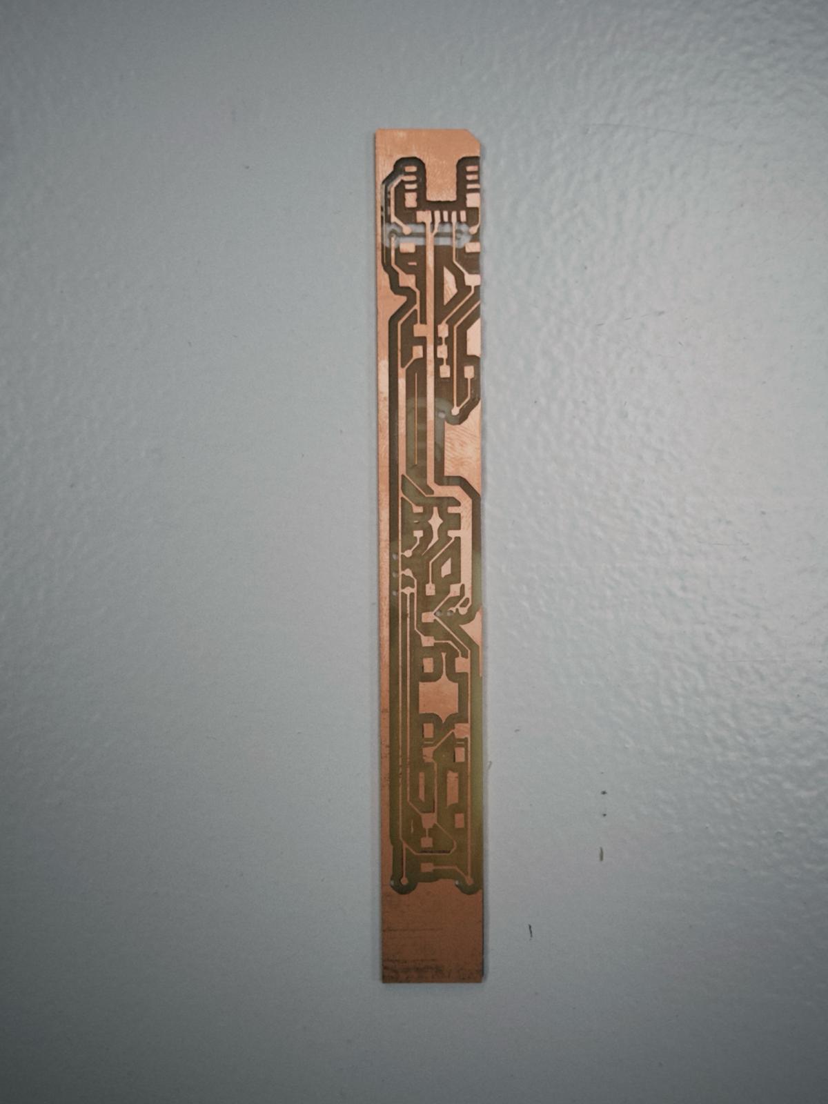
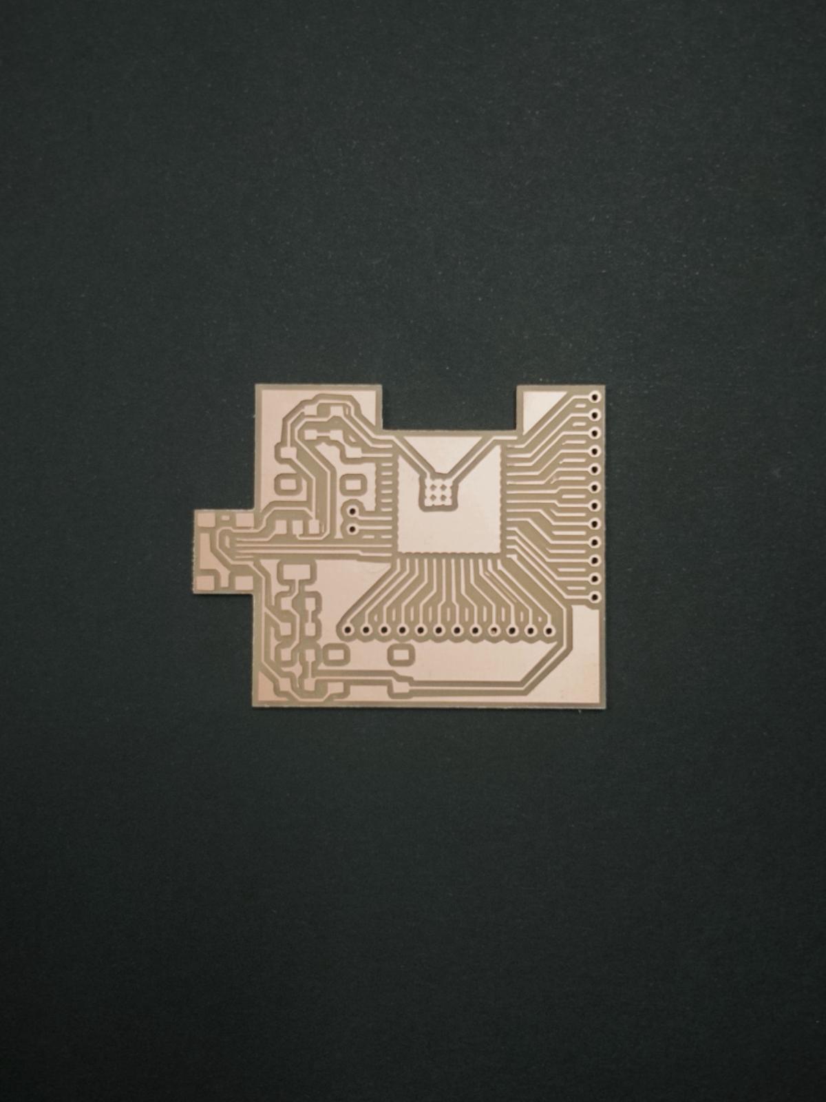
This board looked kinda promising! I added holes to avoid the vias, and everything else seemed nicely connected.
In order to cut all the excess copper of the board (fill cut), I was using a 1/64" mill bit and it was obviously taking a long time. For this one I tried combining traces with 1/64" and then doing the fill with a 1/32" bit, but it seemed like it made my tracks way too thin! So it's a no for next time (either using 1/64" all the way or setting higher tolerances in KiCAD/Rhino). So I couldn't proceed with this design yet, would have to recut it.
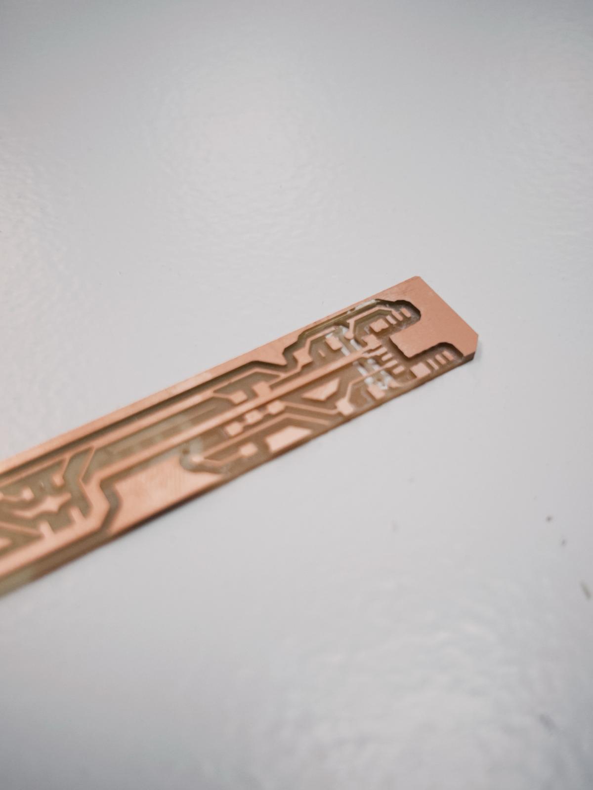
On Monday, Adai helped me troubleshoot the board.
1. Found out there were many short circuits happening. Tried knifing them. Didn't work.
2 Only one resistor would be enough for the LED.
3. I had the wrong LED in.
That solved the LED issue.
But then, found out my computer wouldn't find the board as a COM port!
2.4. My switches also seemed to have some wrong connections... Considered removing them
Haven't found the final solution. Decided to REDESIGN. This time I just want something simple. I'll leave the pro dev board for the pros. This is taking way too long.
Week 11 update:
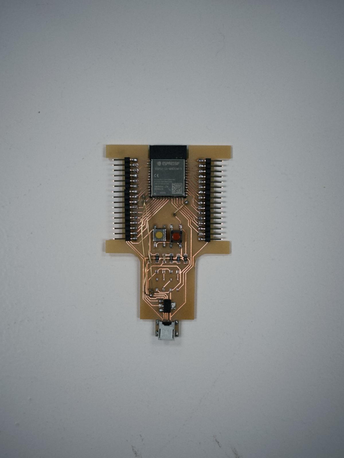
It finally worked! Did a few more design iterations with the goal of simplifying the board - instead of trying to get it to do everything I wanted. Maximed the pin access, but removed the extra LEDs and neopixel. It took a few attempts because I was getting
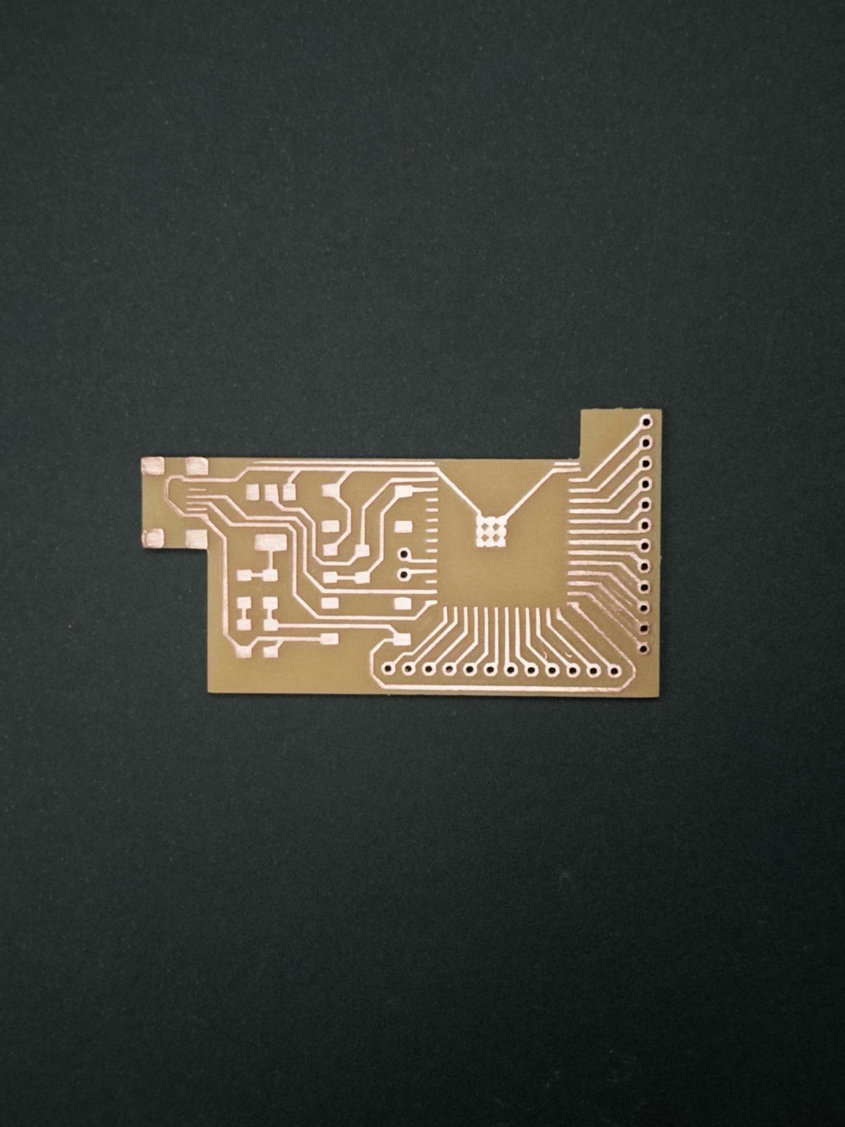
The one on the left was the almost-final design! In this one I had trouble with the data wires connected to the micro USB, and my switches had to be wired in the opposite way I had setup. On the right, I fixed those things and added power and ground pins, which I kept forgetting before! Also, I was ignoring one of the pins (IO8), which would be crucial for I2C communication later on - thankfully I'm working on the input devices assignment on the side I figured this out. The one on the right is the final success, even though the buttons are not aligned. I believe I had to do mess up some aesthetic feature just so that it would agree to work. And it did! Functional crooked board is the one.
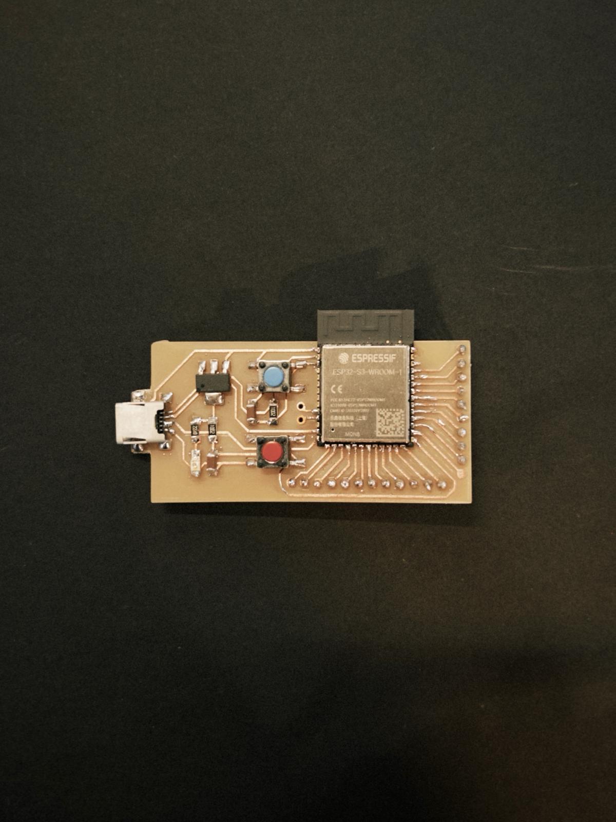
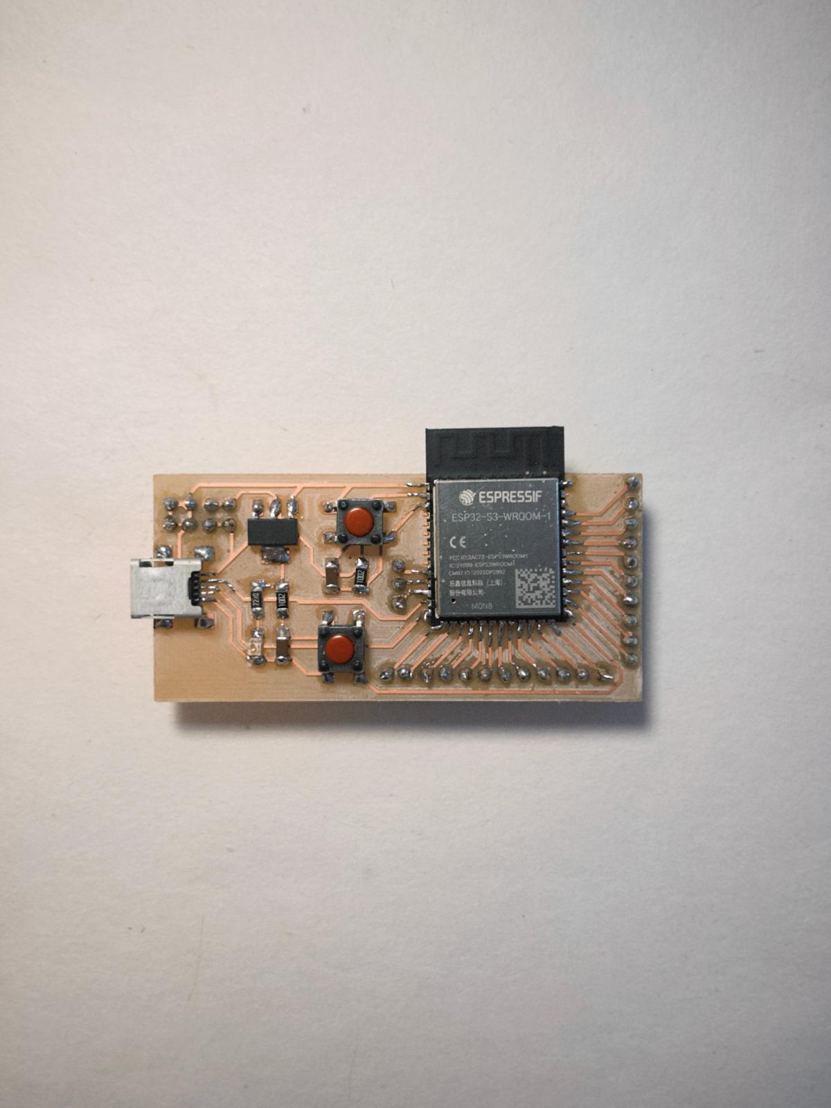
Here is a video showing the board working when pressing the boot button.
Some reference links:
Barduino's pinout: https://fablabbcn-projects.gitlab.io/electronics/barduino-docs/GettingStarted/pinout/
ESP32S3 WROOM 1 Datasheet: https://www.espressif.com/sites/default/files/documentation/esp32-s3-wroom-1_wroom-1u_datasheet_en.pdf
FILES: