Week 8
Electronic Design
Fab Academy 2024
Riichiro Yamamoto
- Group Assignment
- SAMD11
- Components
- KiCad
- Inkscape
- MODs
- Milling
- Program with Platform IO
- Program as a programmer with Arduino
- Blink the SAMD11
- Touch the SAMD11
Dear My Friend
This week I was introduced to Electronic Design, which is selecting components and designing your own PCB. The main goal for this week was to design, fabricate, and program the development board. The development board is a board you use to control other boards.
The basic workflow goes like this
- Decide what you want the development board to do
- Select microcontroller understand Pinpout
- Find out what components you need
- Design the board with Electronic Design Automation (EDA) software(for me KiCad)
- Adjust SVG file in CAD software (for me Inkscape)
- Use MODs to generate files for Milling machine
- Milling PCB
- Program the board
Riichiro Yamamoto
Group Assignment
this week's group assignment was to use the test equipment in your lab to observe the operation of a microcontroller circuit board. Send a PCB out to a board house.
Here is the link to the group assignment page

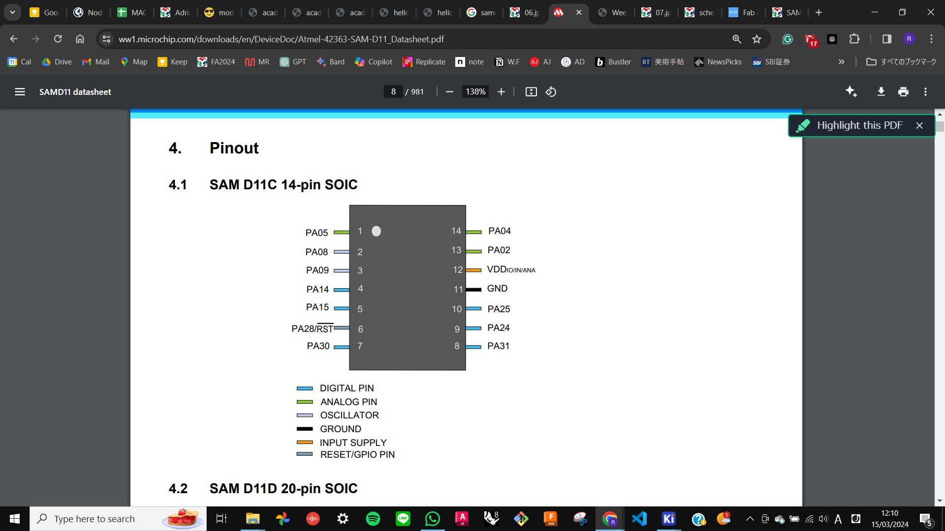
SAMD11
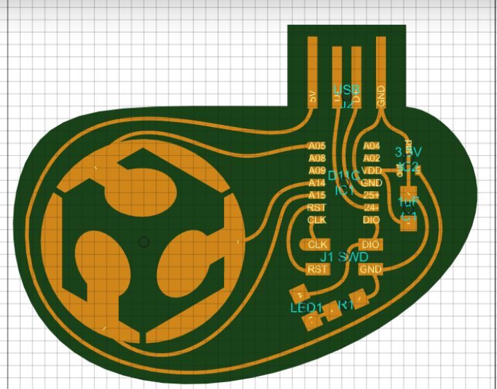
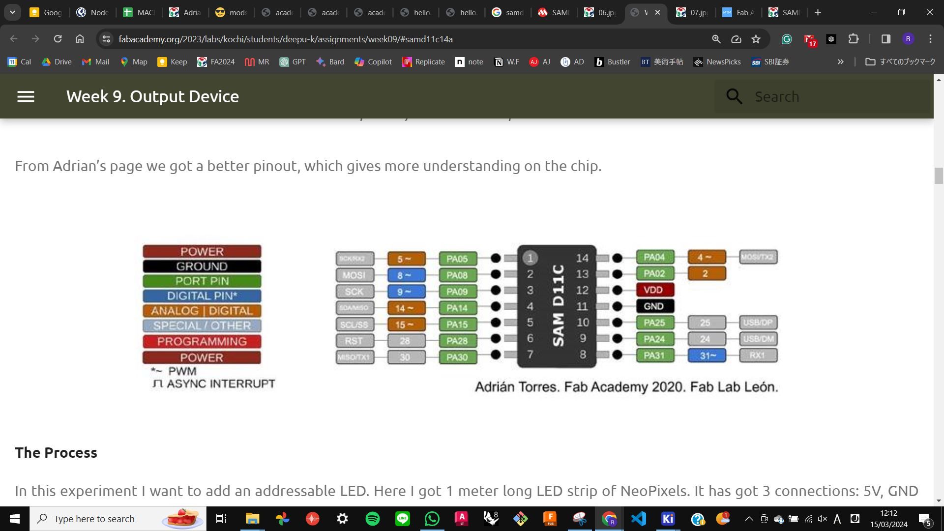
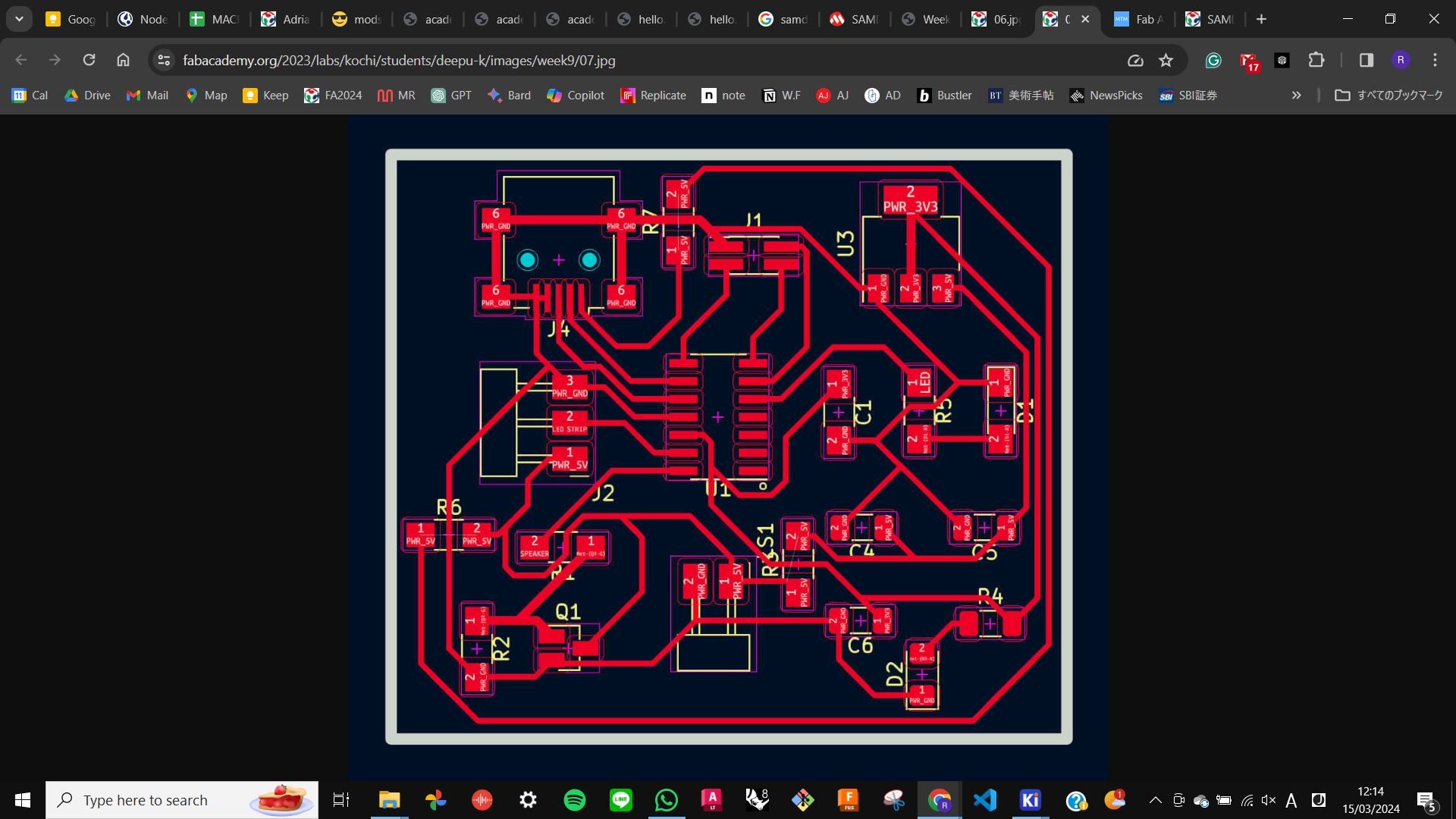
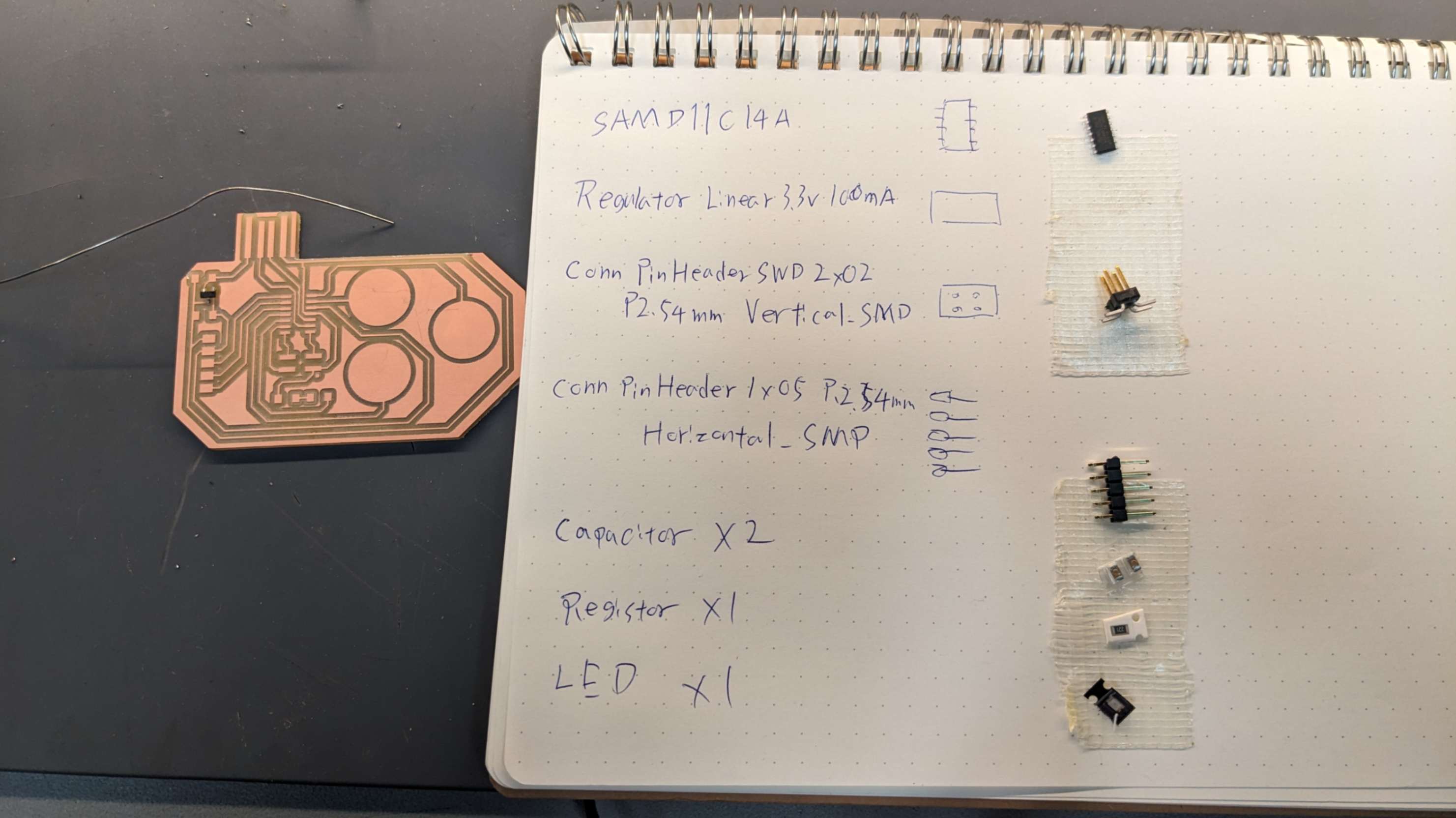
For my PCB, I decided to use SAMD11C14A (SAMD11) because it has many pins and has the PTC peripheral capable of step response touch sensing without any additional hardware. As a reference, I used SVG PCB splines by Quentin Bolsee
Components
By looking at
the reference,
another reference,
DataSheet,
and
SAMDino by Adrian Torres,
I started to understand how my board should work.
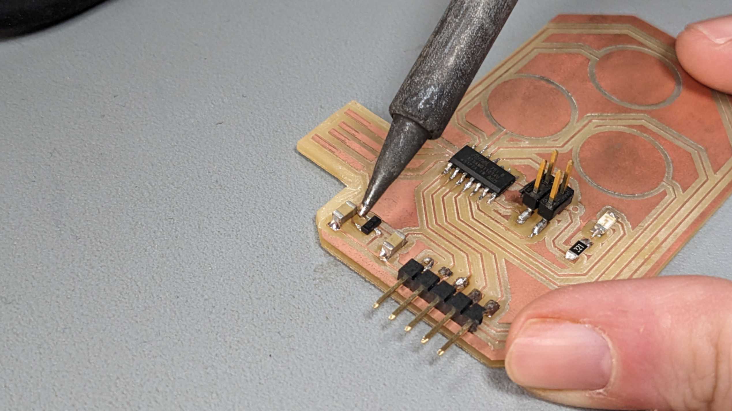
Also, by asking a bunch of questions to my tutors, I finally figured out what components I needed on my board. Below is the list of components.
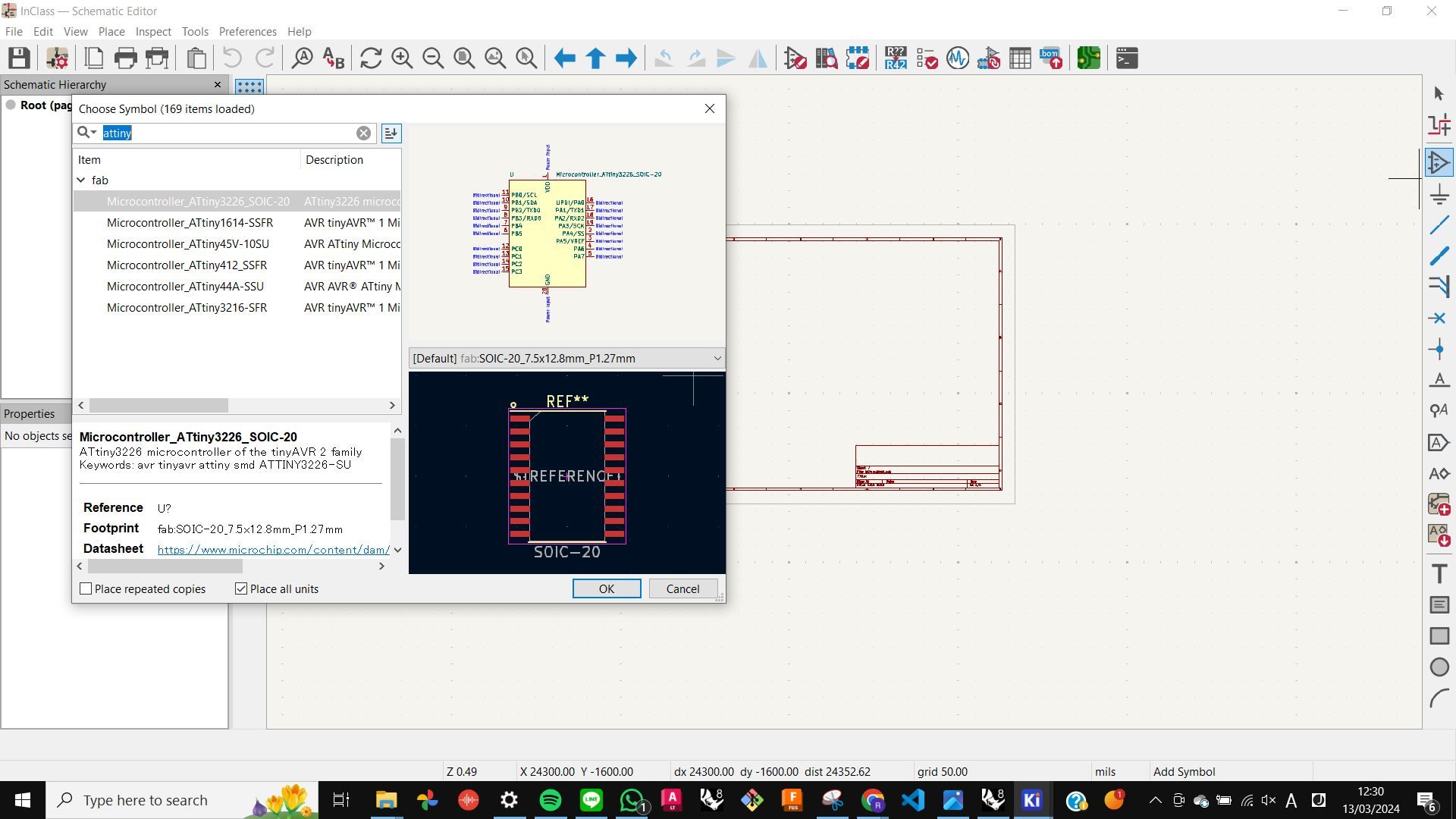
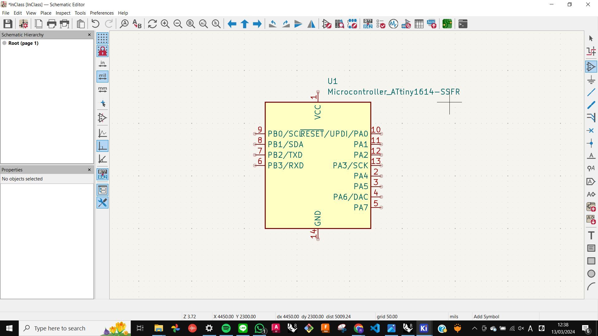
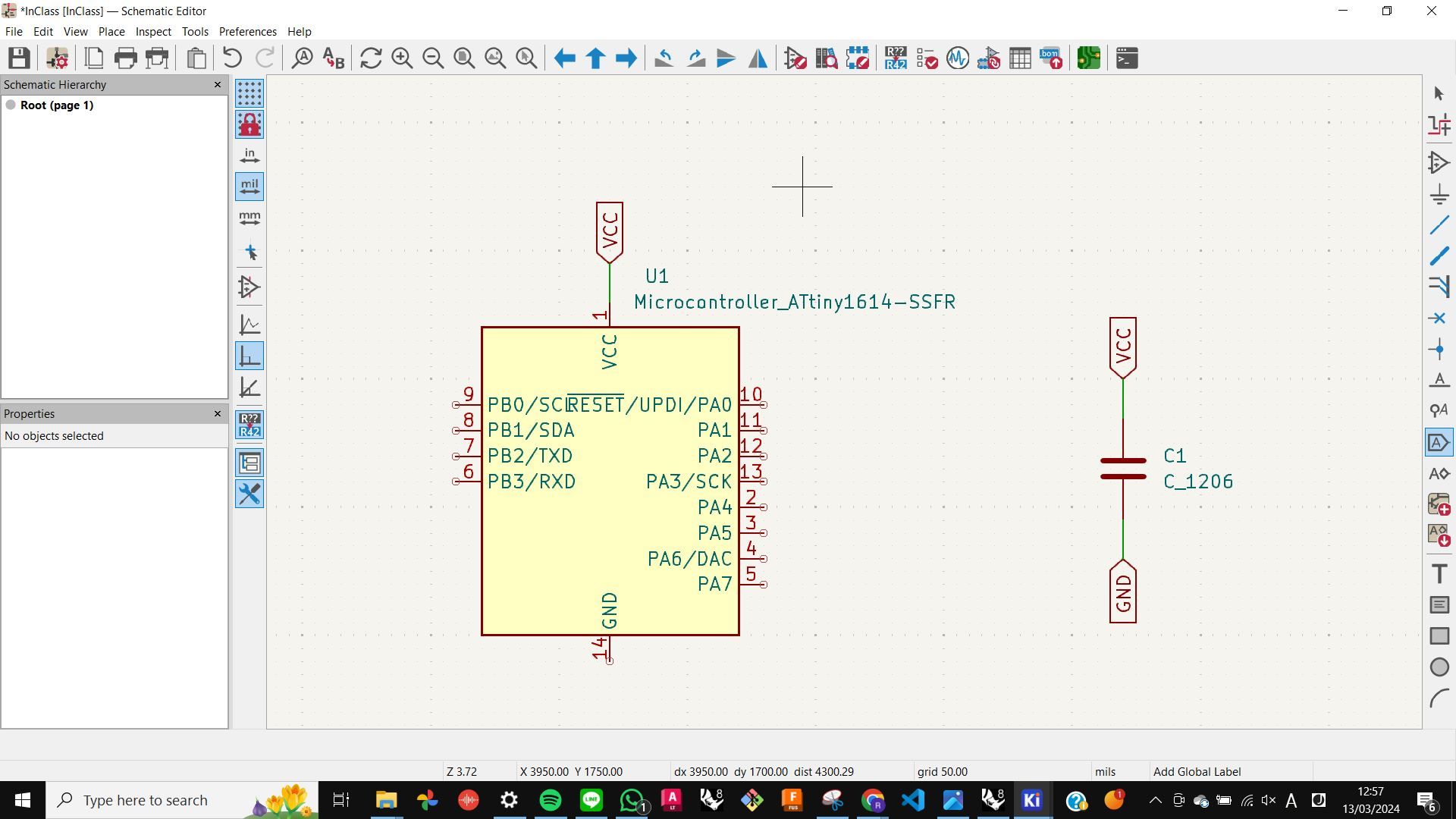
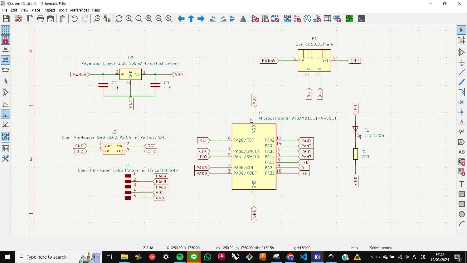
- Microcontroller SAMD11
- USB Connection (for programming directly from PC)
- Voltage Regulator (for converting 5V to 3.3V)
- 2 Capacitor (for voltage regulator)
- SWD Vertical Male Pin (for programming though RP2040)
- 5 Horizontal Male Pin(for connecting additional board)
- LED (for checking )
- Registor (for LED)
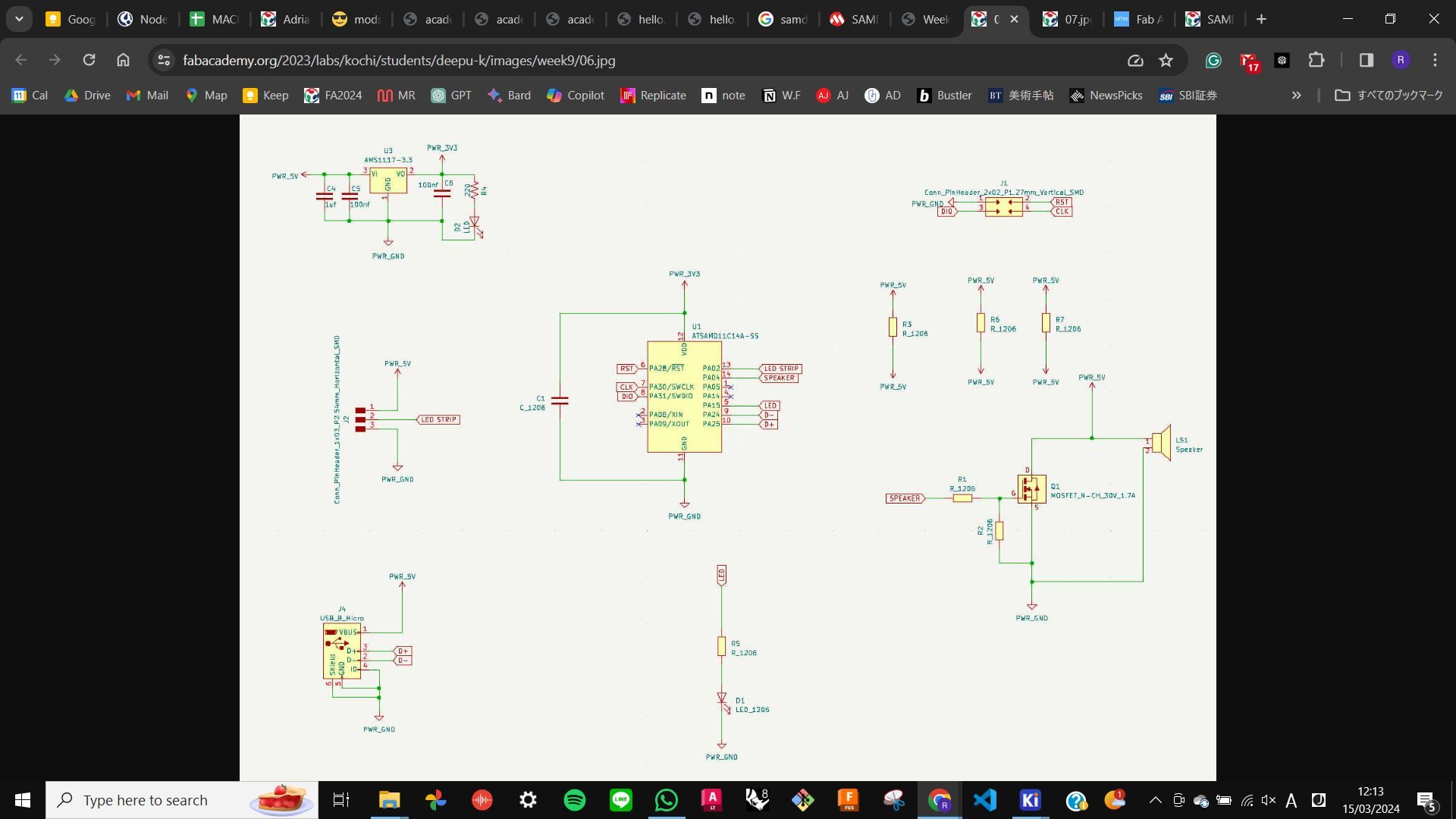
KiCad
I was recommended to use KiCad for making schematics and tracing for PCB, because our lab environment aligns with it. Below is the workflow of KiCad.
Install & Set UpLibrary
- Install KiCad
- Open Kicad
- Download as Kicad Fab Library from this page this page as a Zip file
- It is important to know the location of the Zip file because KiCad will reference it
- Preference, Manage Symbol Libraries
- Only for the first time, Choose Copy Full Global Symbol Libraries
- it will load all the default libraries
- Select all the libraries, and press the space key to deactivate, (good to do this because it takes time to load every time if they are active)
- Activate only the library you want to use( also it makes easier to find components)
- There are Global Library and Project Specific Library, for now, Global Library is good. If you have a library only for specific projects then have it in Project Specific Library
- Add Library, go to the Zip file, and look for a file named fab.kicad_sym
- Make sure the Fab library is active and close the window
- Preference, Manage Footprint Libraries
- Only for the first time, Choose Copy Full Global Footprint Libraries
- it will load all the default libraries
- Select all the libraries, and press the space key to deactivate
- Add Library, go to the Zip file, and look for a folder named fab.pretty
- Make sure the Fab library is active and close the window
- Now KiCad has Symbol Library and Footprint Library ready to be used
Files
Custom.kicad_pro
Custom.kicad_sch
Custom.kicad_pcb
Schematic
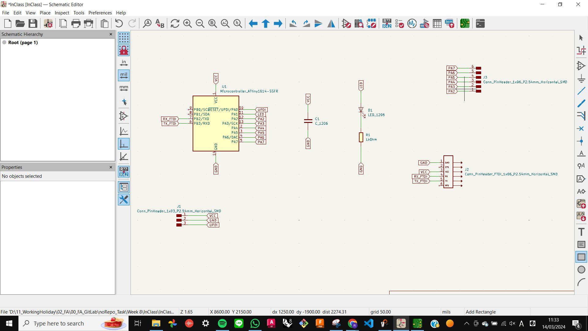
- Go to Schematic Editor
- Add components by Add Symbols (A)
- Add label by Add global labels (Ctrl+L)
- Connect components and labels by Add a wire (W)
- Adjust placements to understand easier
- Move on to PCB Footprint by Open PCB in board editor button
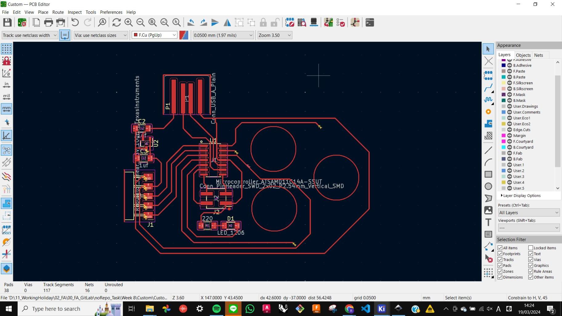
PCB Footprint
- Update PCB with change made toschematic
- Place all the footprint
- Adjust placement by Move (M), Rotate (R), Grab (G) and Flip (F)
- See blue line for connection
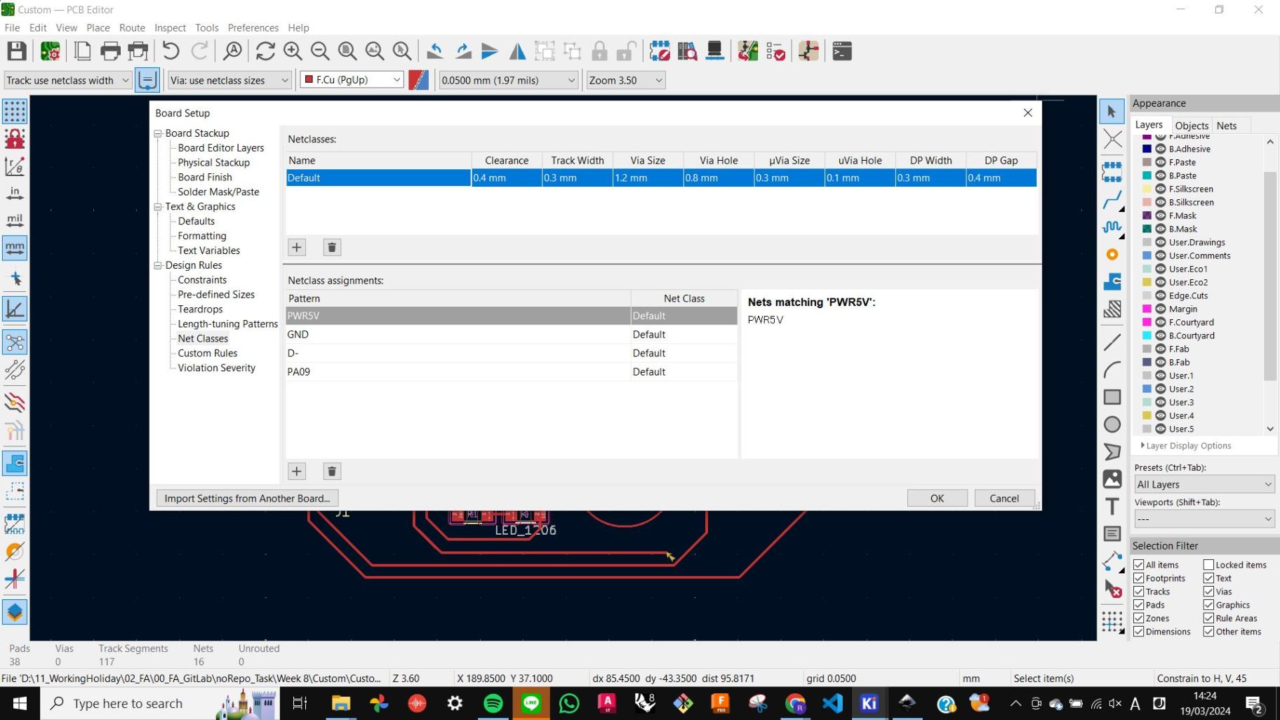
- File - Board Setup - Net Classes
- Change default parameters
- Clearance 0.4mm, Track Width 0.3mm, Via Size 1.2mm, Via Hole 0.8mm, uVia Size 0.3mm, uVia Hole 0.1mm, DP Width 0.3mm, DP Gap 0.4mm
- Draw trace by Route track (X)
- Change labels and orders in schematic if necessary
- Update PCB every time change made to schematic
- Check for errors and warnings by Design Rules checker window
- dont have to worry about warnings
- Fix errors unless it is expected
- Export as SVG file
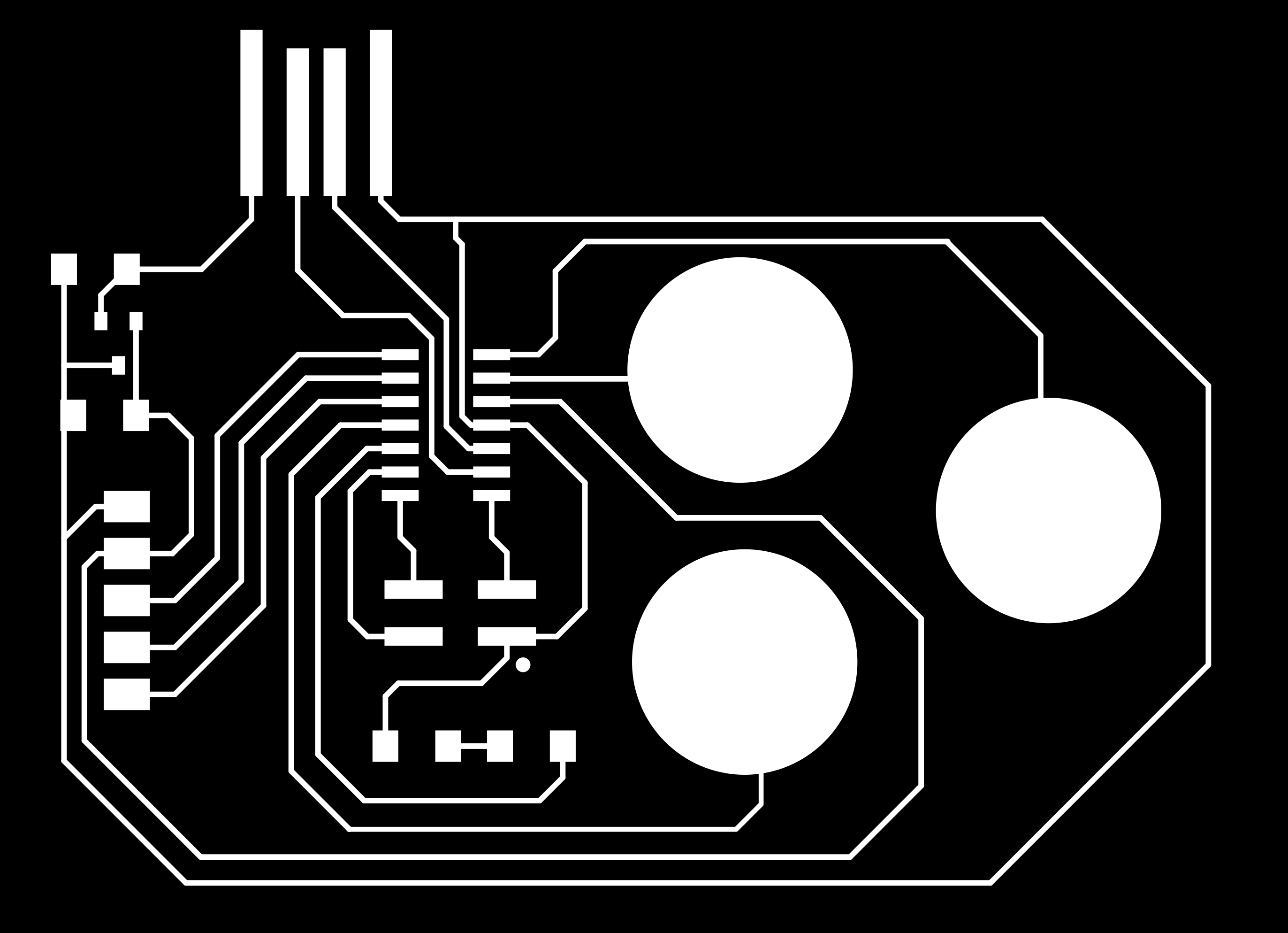
Inkscape
- Open SVG file in Inkscape
- Defferenciate trace & footprint, holes, and outline
- Make layer for trace, holes, outline
- Move to layers according to what it is
- Make Background layer, create black background (Change opacity to see easier)
- Change stroke to white, fill to none for trace
- Change stroke to none, fill to white for footprint
- Change stroke to black, fill to white for outline
- Change stroke to white, fill to black for holes
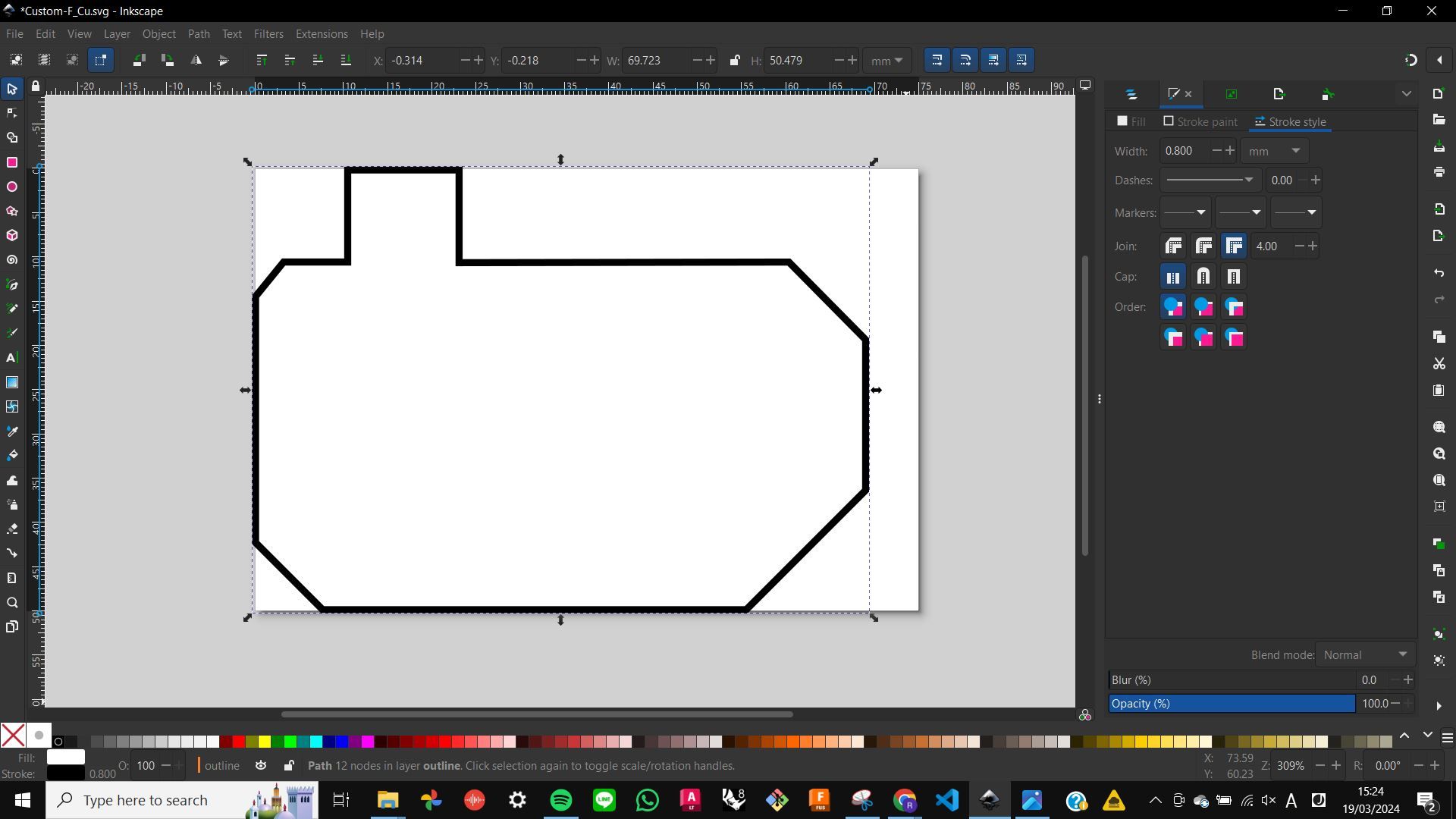
- Draw an outline with 0.8mm thickness
- Exporting should be PNG with DPI 1000
- Export with outline size by Selection. Always export in the same size
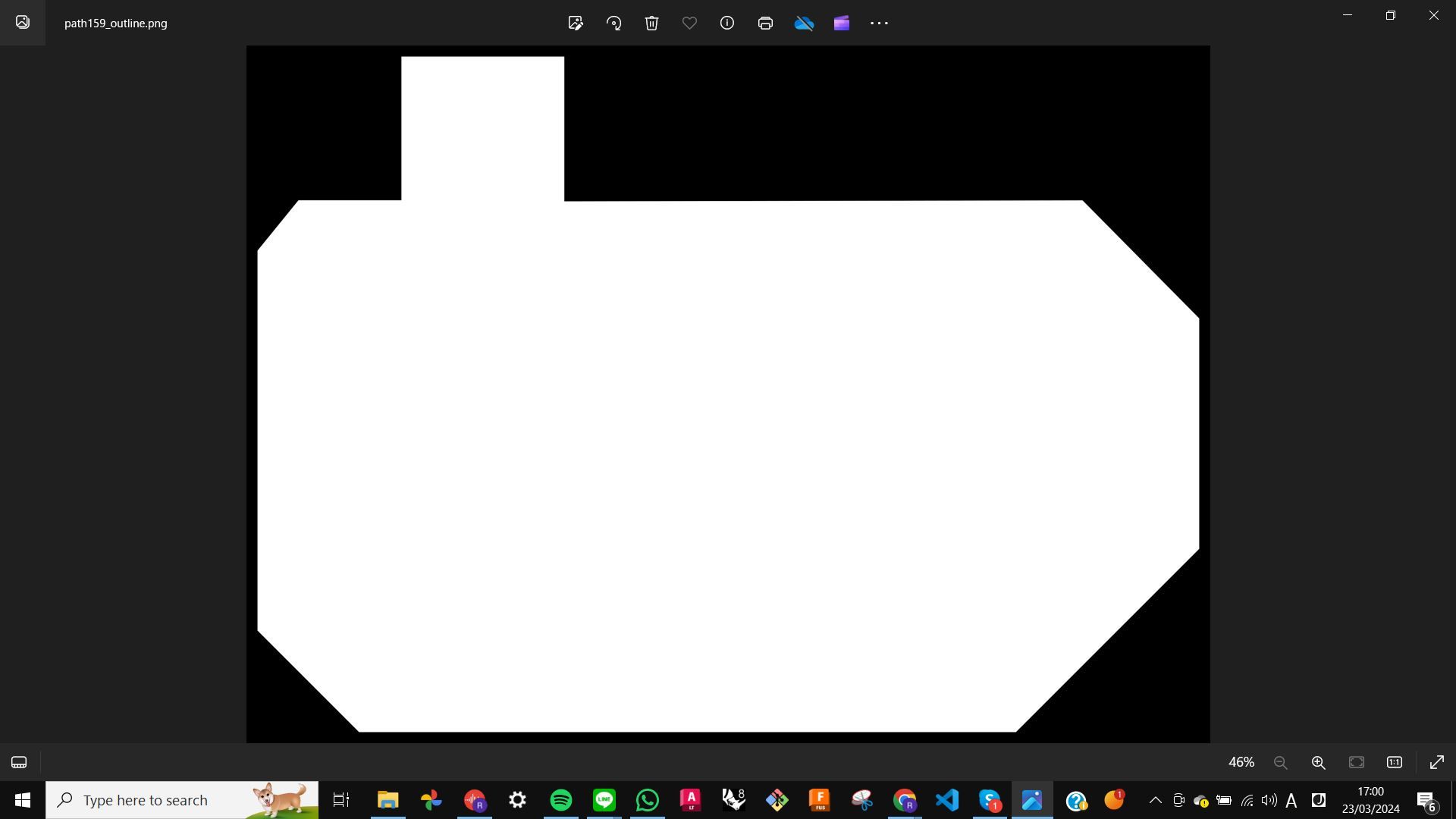
- Export outline with background
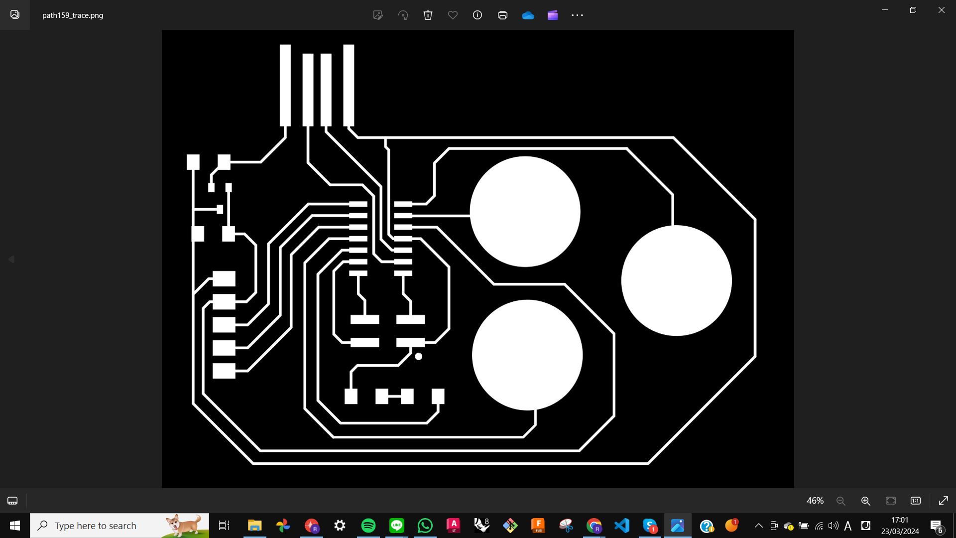
- Export trace with background
- Export holes with background
- Move on to MODs
Files
Custom-F_Cu.svg
path159_outline.png
path159_trace.png
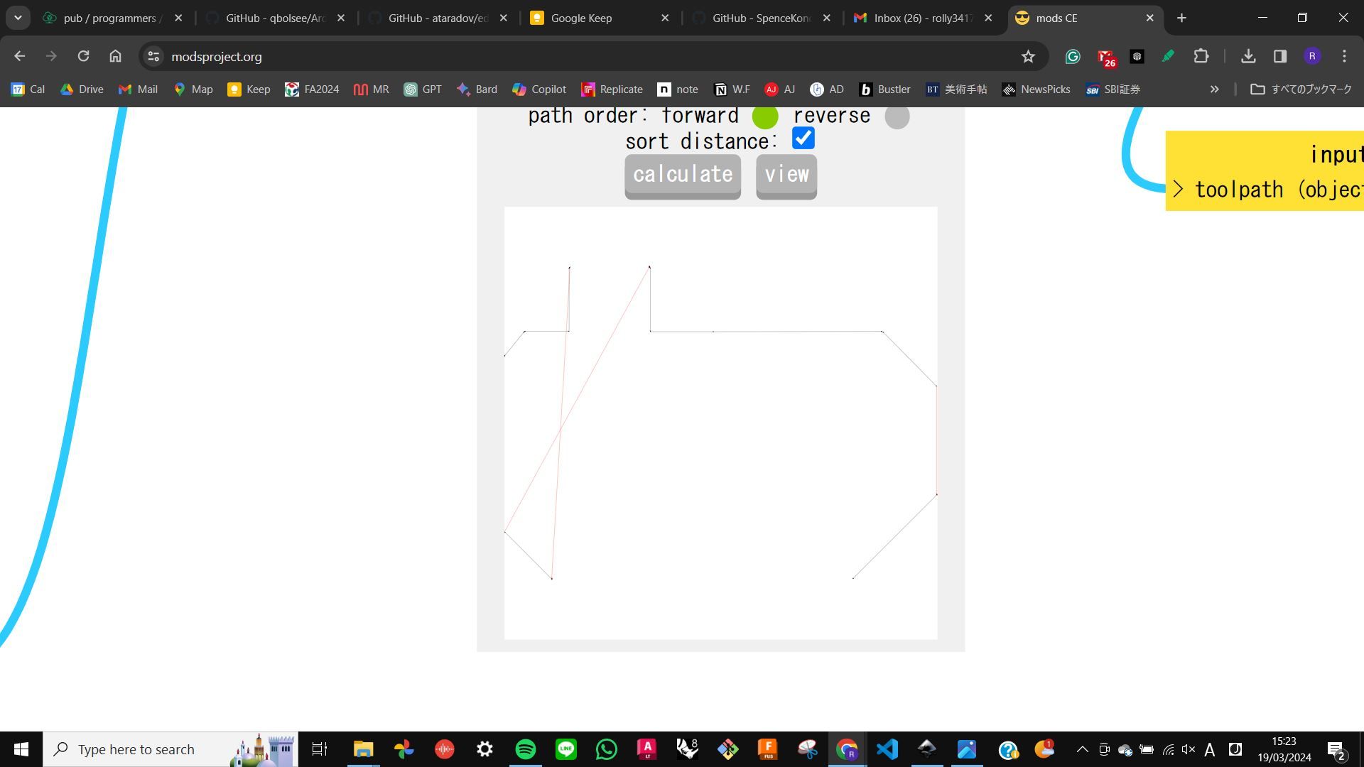
MODs
I used MODs to prepare files for milling. I did this with the same workflow from Week 4 Electronic Production
Problem
A problem I had during this phase was that my milling preview was showing unnecessary cuts for the outline. It was caused by the outline PNG not having a transparent background so MODs were acting weird. Simply I added a black background to fix this issue.
Files
path159_outline.png.rml
path159_trace.png.rml
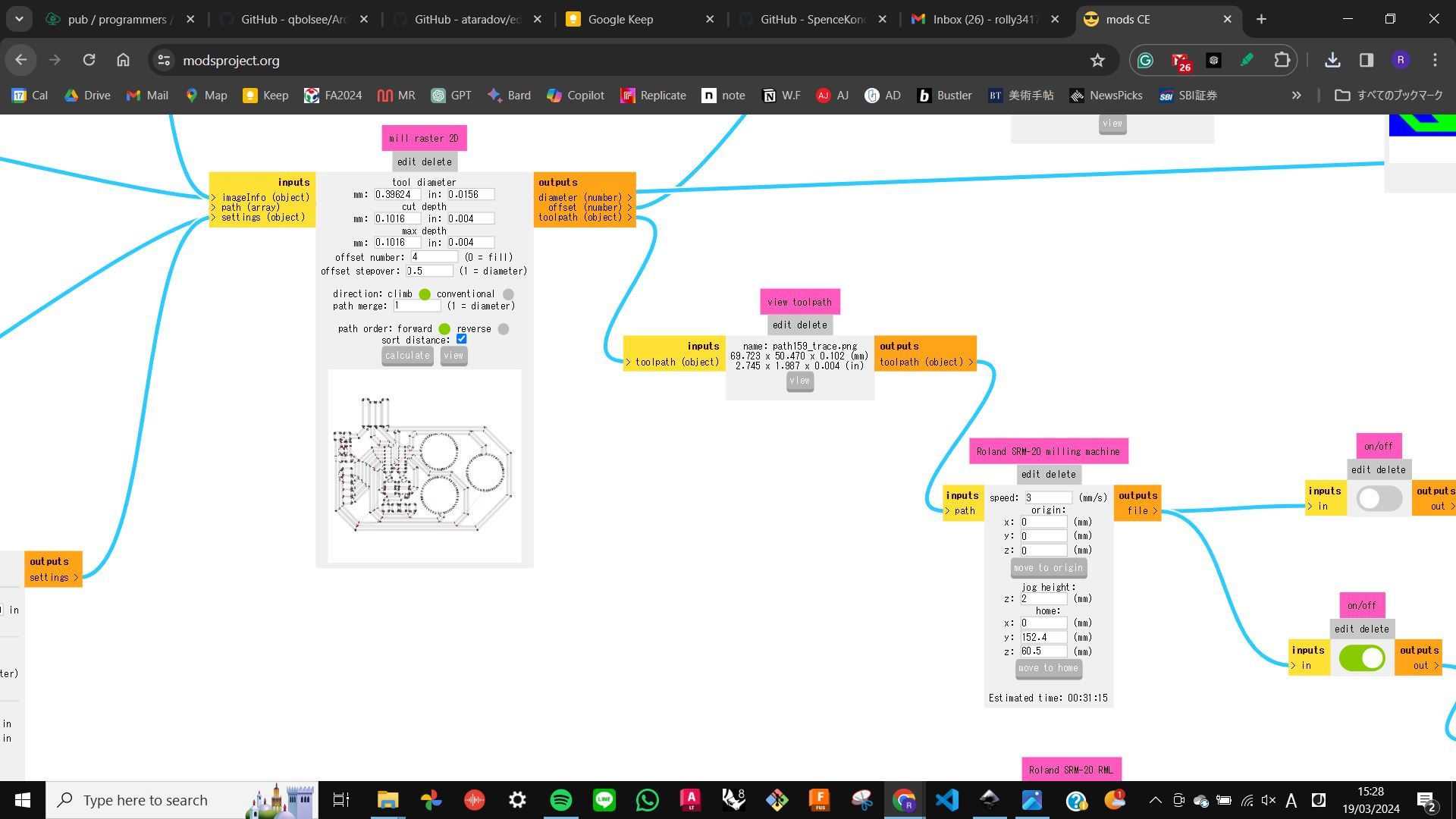
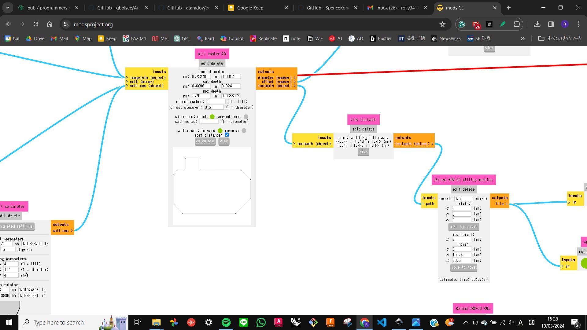
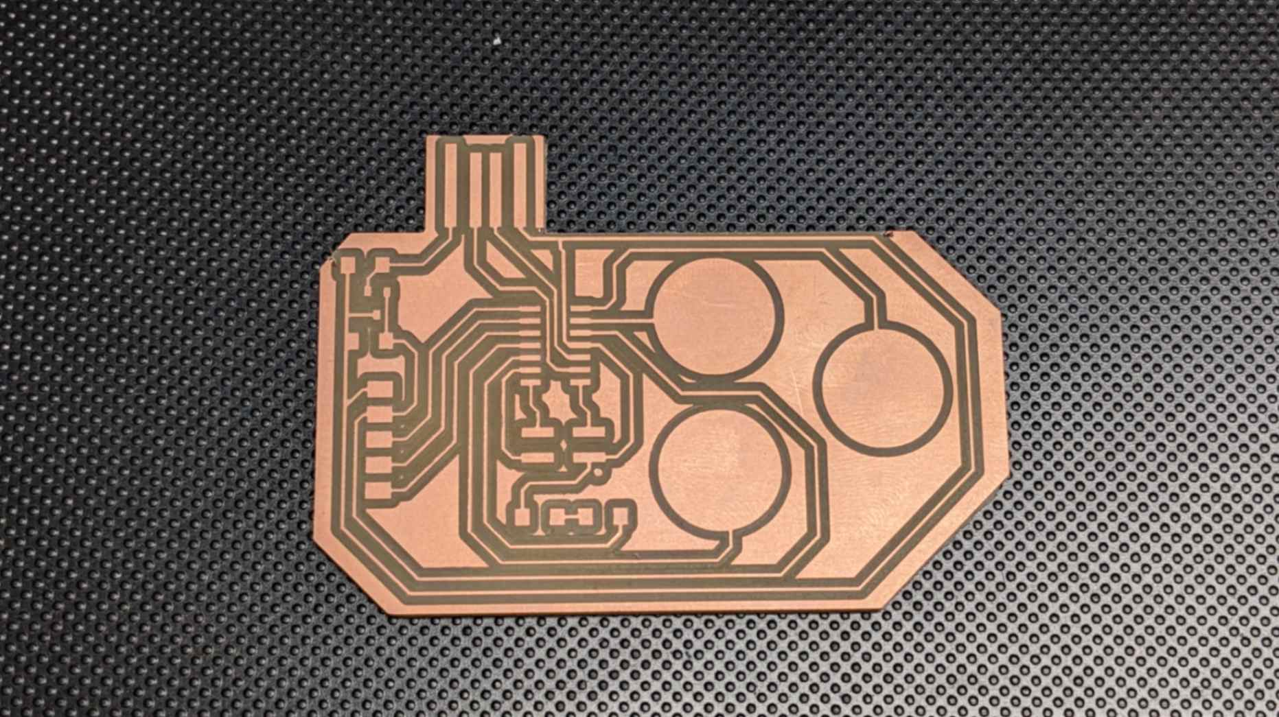
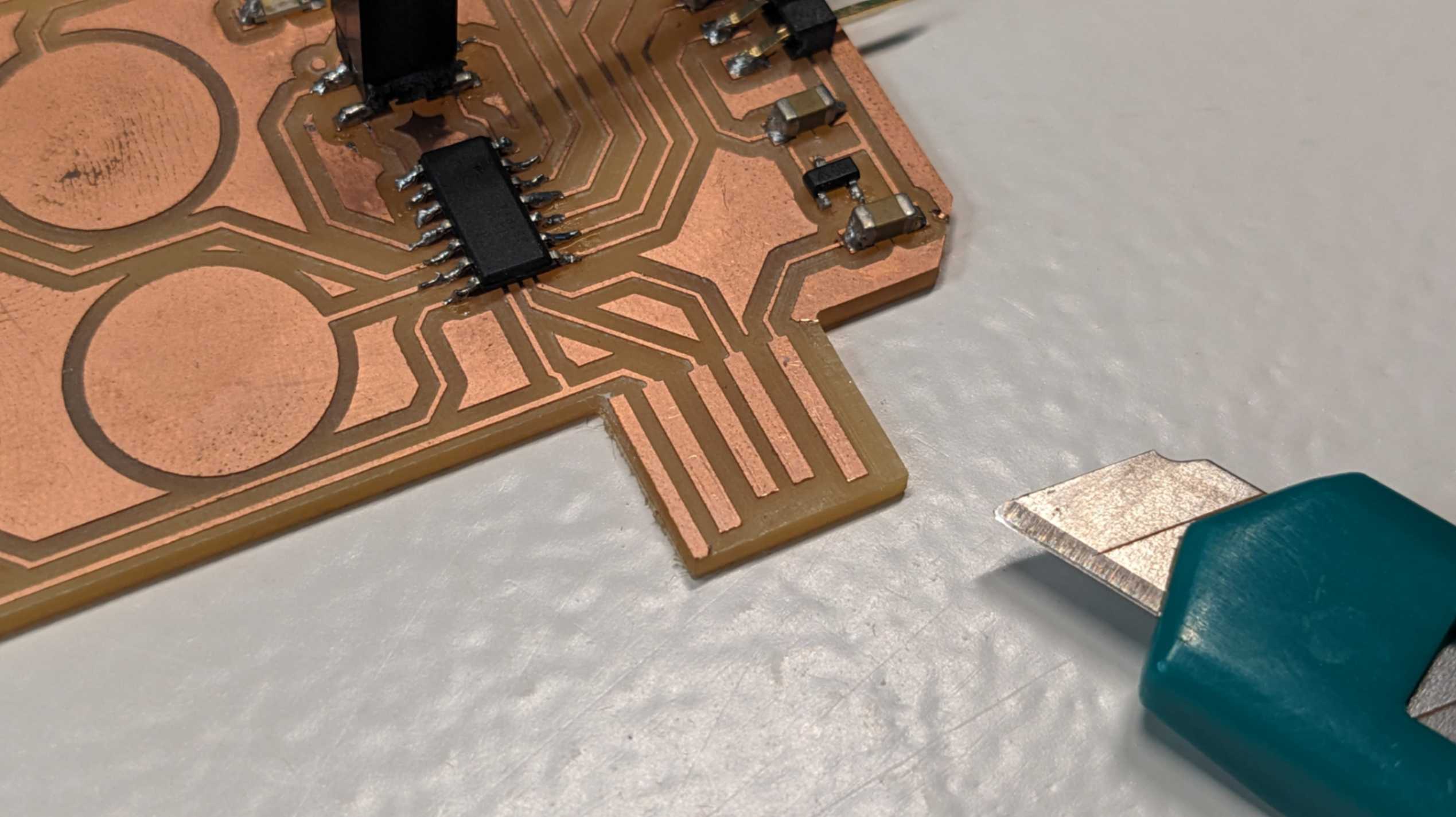
Milling
Again. I did this with the same workflow from Week 4 Electronic Production
A small Trick I learned
My first trial for milling trace was not milling through the copper layer, and I could see shiny traces. I asked for help to my tutor and he told me this trick. While the end mill is milling when the Z axis is -0.10mm, cancel the job, and the end mill will stop in the place. Use the current Z-axis value (-0.10mm) to reset the Z origin, so the next job will be milled 0.10mm deeper. Don't forget to move the end mill up after setting the origin and before you move anything.
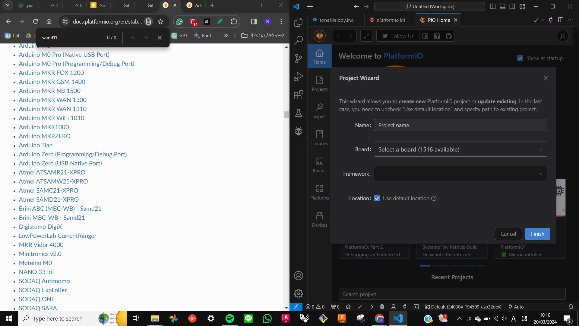
Program with Platform IO
Problem
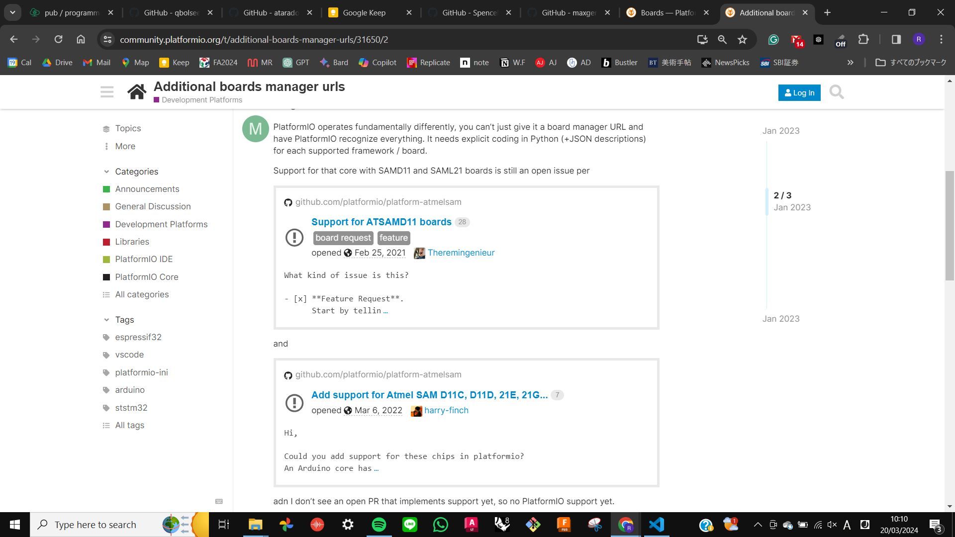
After milling and soldering, it was time for programming. I was going to use PlatformIO since I had a super long compiling sketch time problem with Arduino. However, I could not find a SAMD11 to select as a board. There was only SAMD21. After quick research on this issue,
I found out that the board support for SAMD11 was
previously requested
by users and it has not been updated yet.
After I discussed this problem with my tutor, he advised me to try Arduino once again.
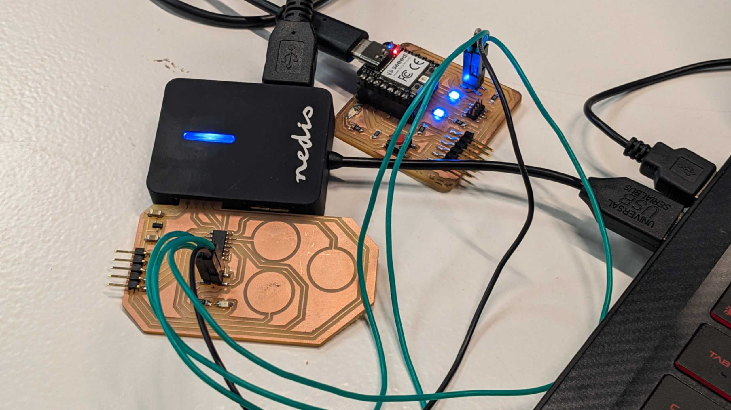
Program as a programmer with Arduino
To flash SAMD11 and make it a programmer, I needed to use another board to flash SAMD11. In this case, I used Quentorres PCB with XIAO RP2040 which I made during
Week 4 Electronic Production.
To use Quentorres as a SWD programmer to flash SAMD11, I simply followed
the How to Use as a Programmer guide
made by Adrian Torres.
The workflow is below.
- Download the uf2 file from here
- Connect Quentorres to PC
- Boot & Reset Quentorres
- PC will read Quentorres as USB and open its folder
- Place the uf2 file inside the folder
- Quentorress will reset automatically
- Now it should be a functional SWD programmer
The workflow is below.
- Solder 4 vertical pins on the blank trace of the Quentorres
- Connect those 4 pins to 4 pins of SAMD11 PCB with 4 wires
- 4 pins are GND, DIO, CLK, and RST
- Make sure they are connected with the same pin because orientation matters
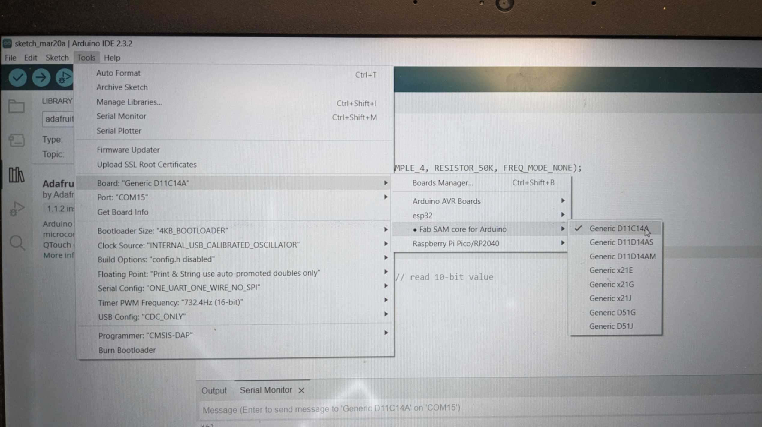
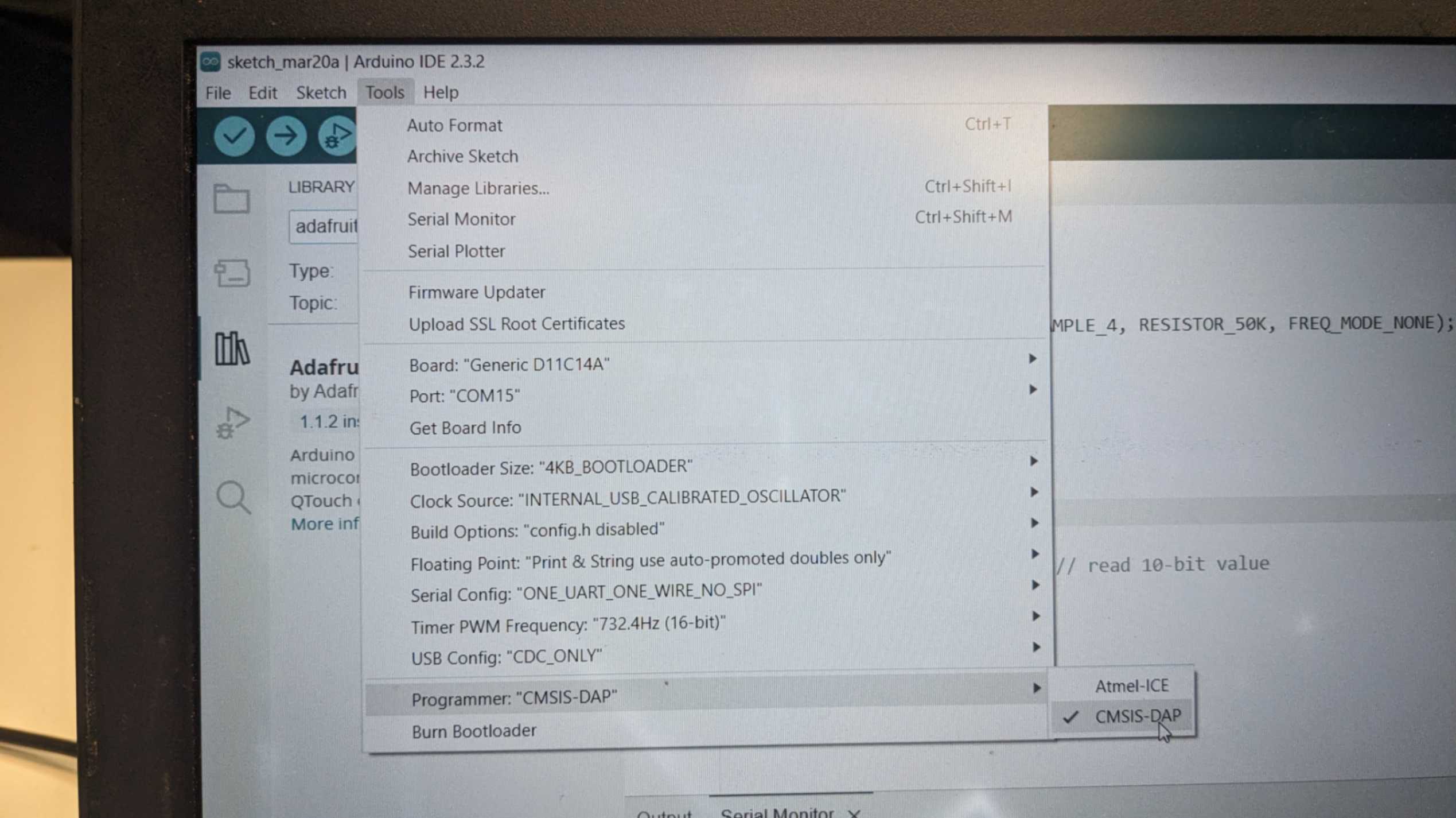
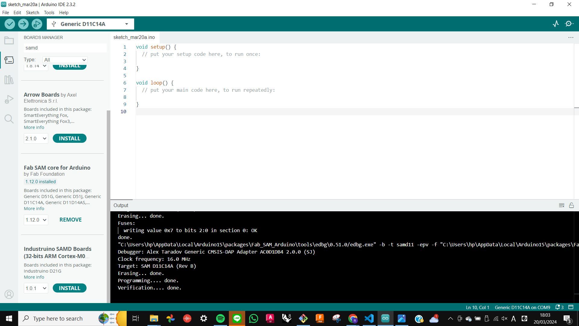
- Copy URL shown in FAb SAM core for Arduino
- Open Ardurino
- File - Preference - Additional board manager URLs
- Paste the URL of FabSAM core
- Select Generic D11C14A in board manager
- Change programmer to CMSIS-DAP from Tool tab
- Select USB port
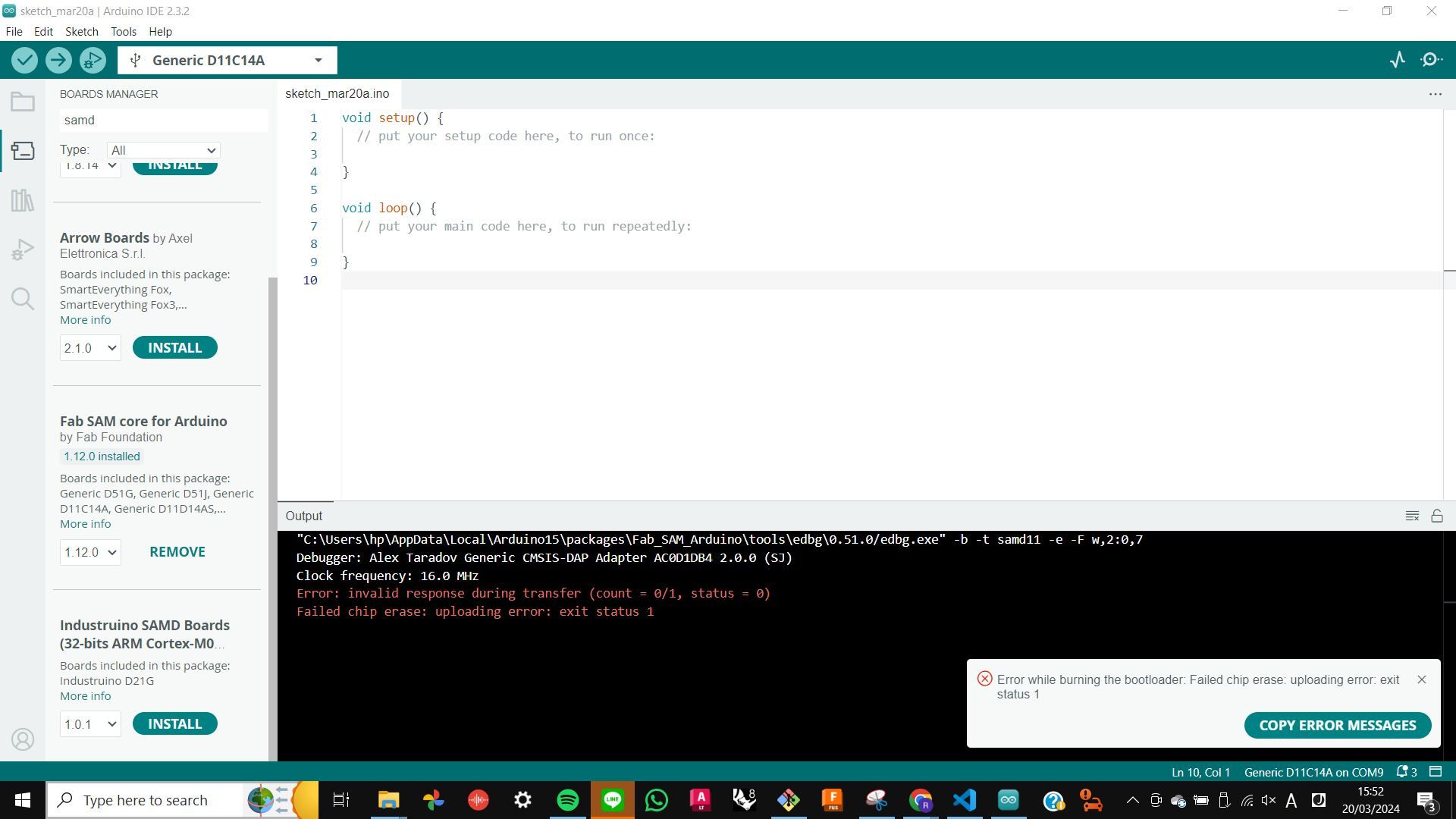
- Burn Bootloader from Tool Tab
Problem
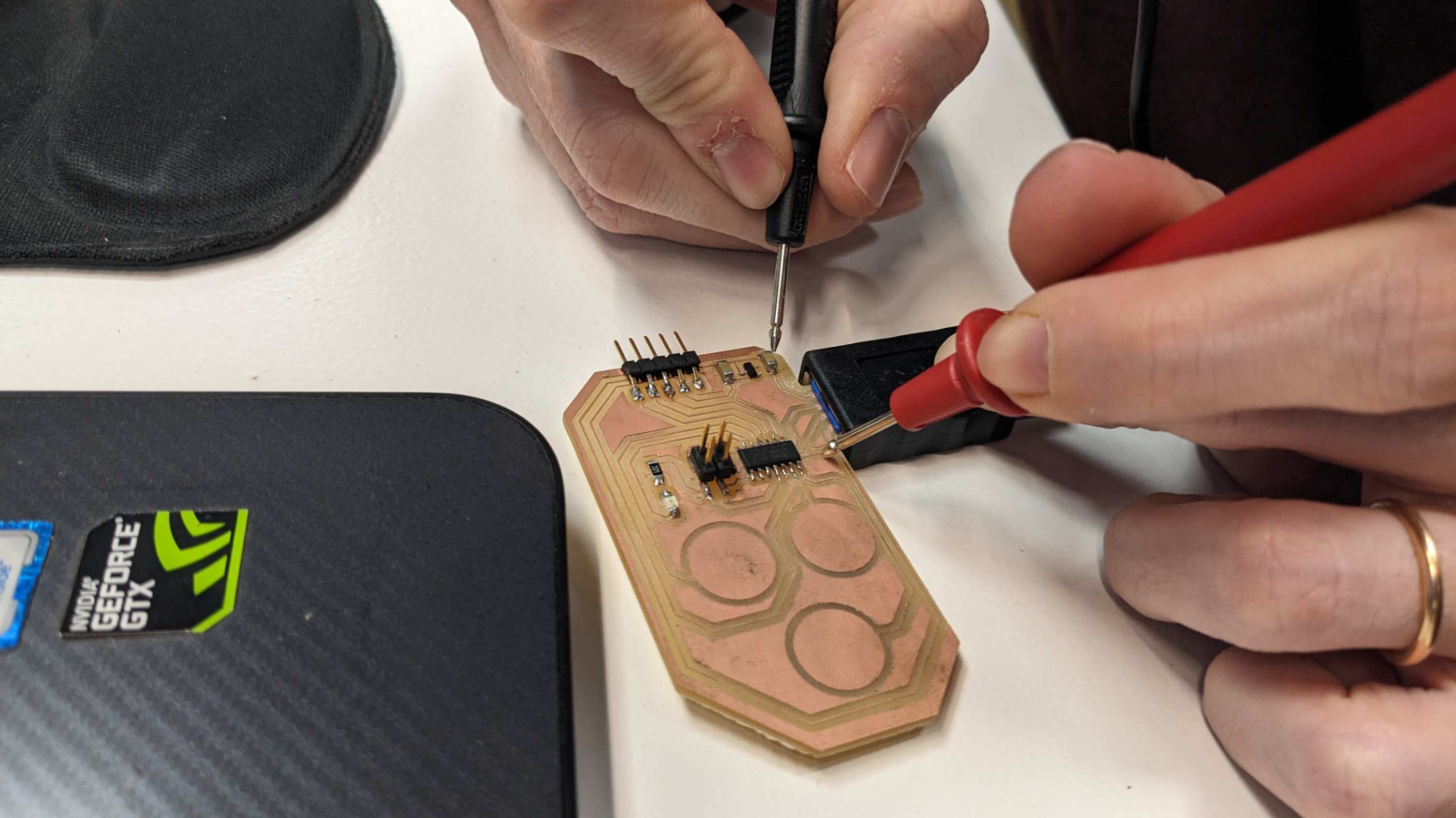
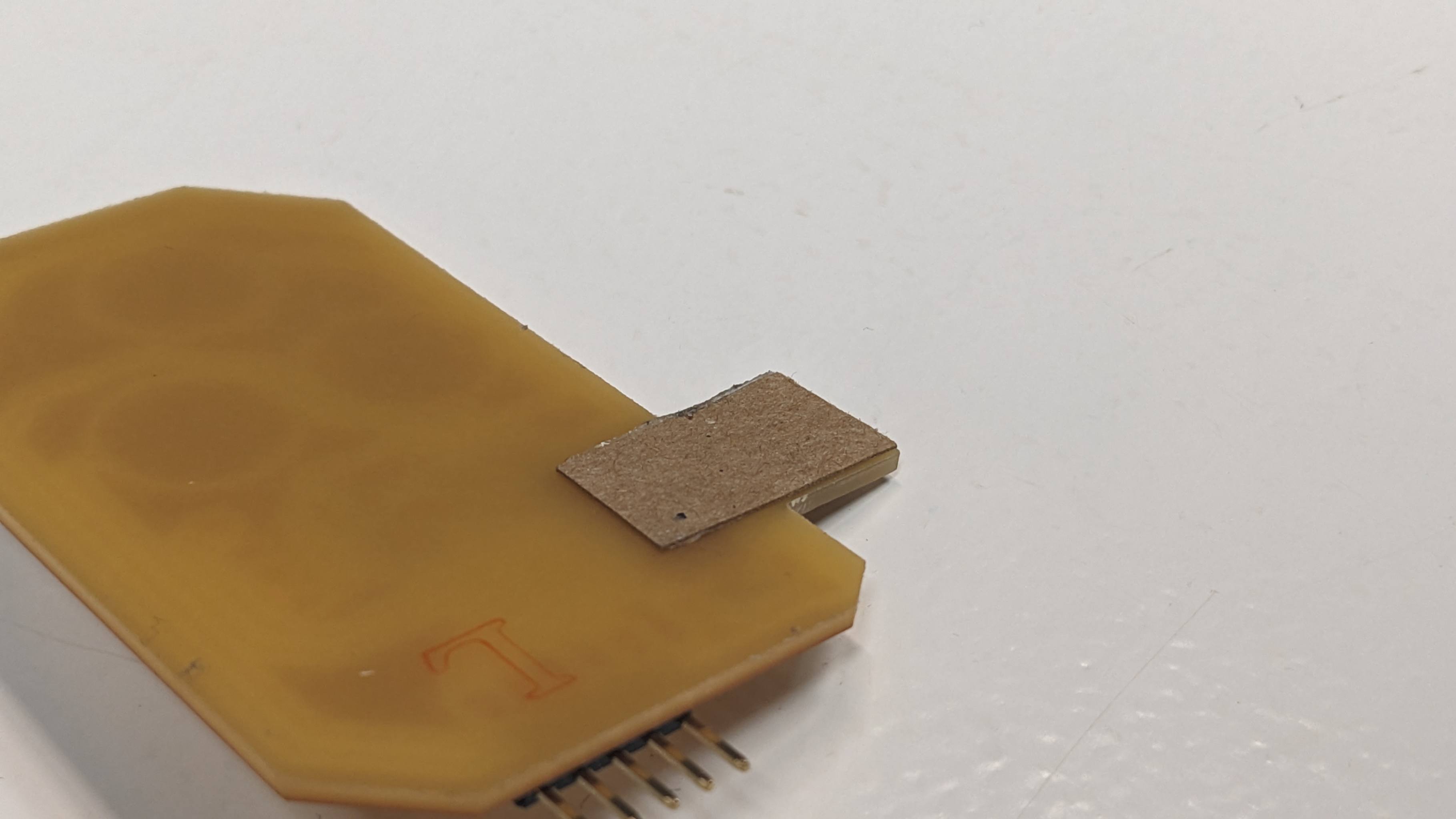
I was not able to burn the bootloader for the first time. The error message was saying something like there was no response from the SAMD11 side, so I assumed the might be something wrong with my SAMD11 board. I checked the connection with the multimeter. They also scraped unnecessary copper around the USB port and added card paper underneath to fit nicely into the USB port. Still, it was showing me the error. Then my tutor checked my components carefully and found the component that I thought voltage regulator was not a voltage regulator. My tutor replaced it and I was able to burn the bootloader.
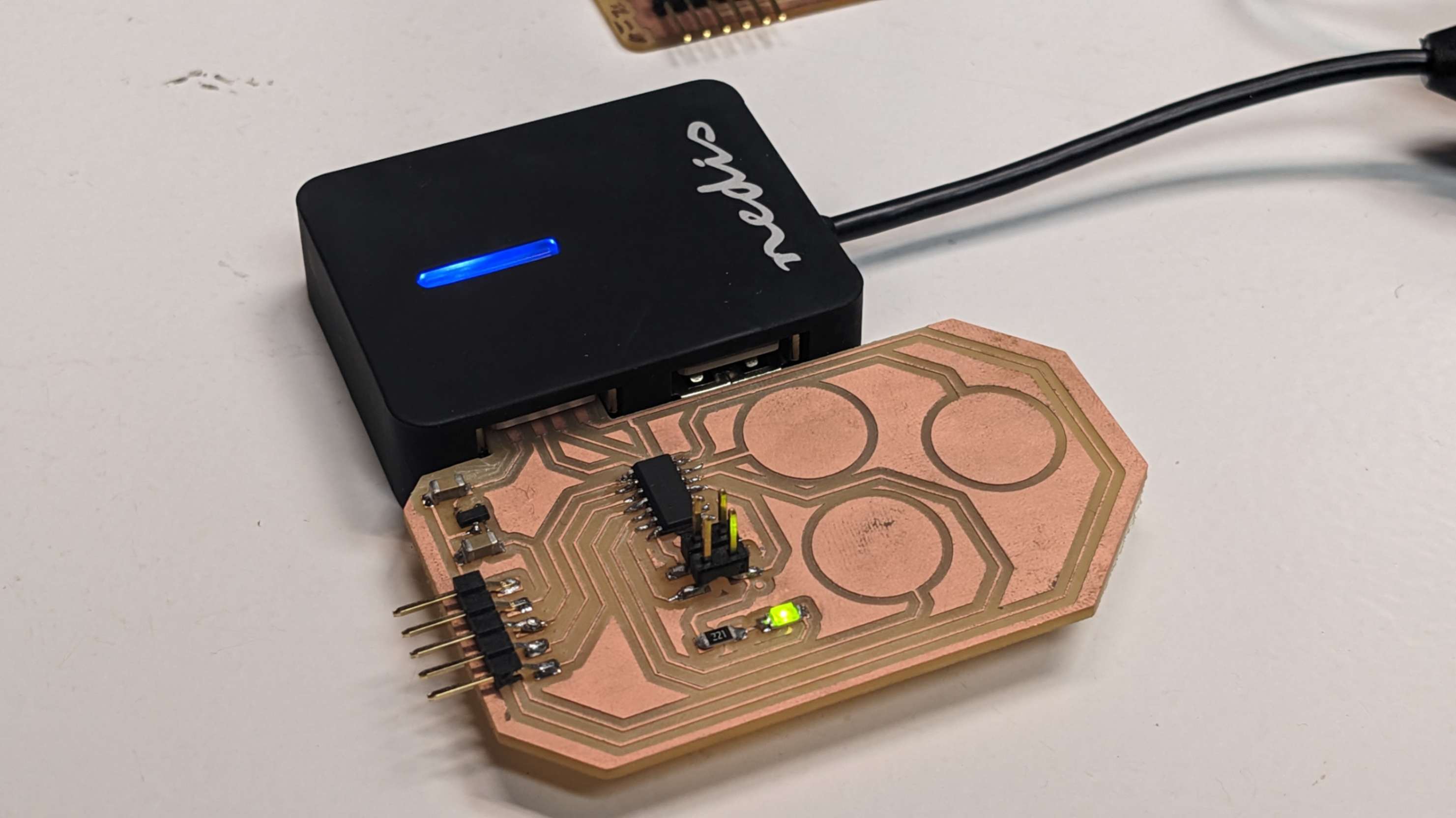
Blink the SAMD11
After bunning the bootloader, I was able to directory program SAMD11. First I did a Blink example as a quick test. Thankfully this time Ardurino did not take a long time to compile the sketch, so it means I can finally play with programming in Arduino.
/*
                Blink

                Turns an LED on for one second, then off for one second, repeatedly.

                Most Arduinos have an on-board LED you can control. On the UNO, MEGA and ZERO
                it is attached to digital pin 13, on MKR1000 on pin 6. LED_BUILTIN is set to
                the correct LED pin independent of which board is used.
                If you want to know what pin the on-board LED is connected to on your Arduino
                model, check the Technical Specs of your board at:
                https://www.arduino.cc/en/Main/Products

                modified 8 May 2014
                by Scott Fitzgerald
                modified 2 Sep 2016
                by Arturo Guadalupi
                modified 8 Sep 2016
                by Colby Newman

                This example code is in the public domain.

                https://www.arduino.cc/en/Tutorial/BuiltInExamples/Blink
              */

              const int ledpin = 15;

              // the setup function runs once when you press reset or power the board
              void setup() {
                // initialize digital pin LED_BUILTIN as an output.
                pinMode(ledpin, OUTPUT);
              }

              // the loop function runs over and over again forever
              void loop() {
                digitalWrite(ledpin, HIGH);  // turn the LED on (HIGH is the voltage level)
                delay(1000);                      // wait for a second
                digitalWrite(ledpin, LOW);   // turn the LED off by making the voltage LOW
                delay(1000);                      // wait for a second
              }
Touch the SAMD11
Next, I wanted to play with the TouchPad that I included on the board. I followed
the
SVG PCB spline
by Quentin Bolsee and was able to blink LED by TouchPad.
The workflow is below.
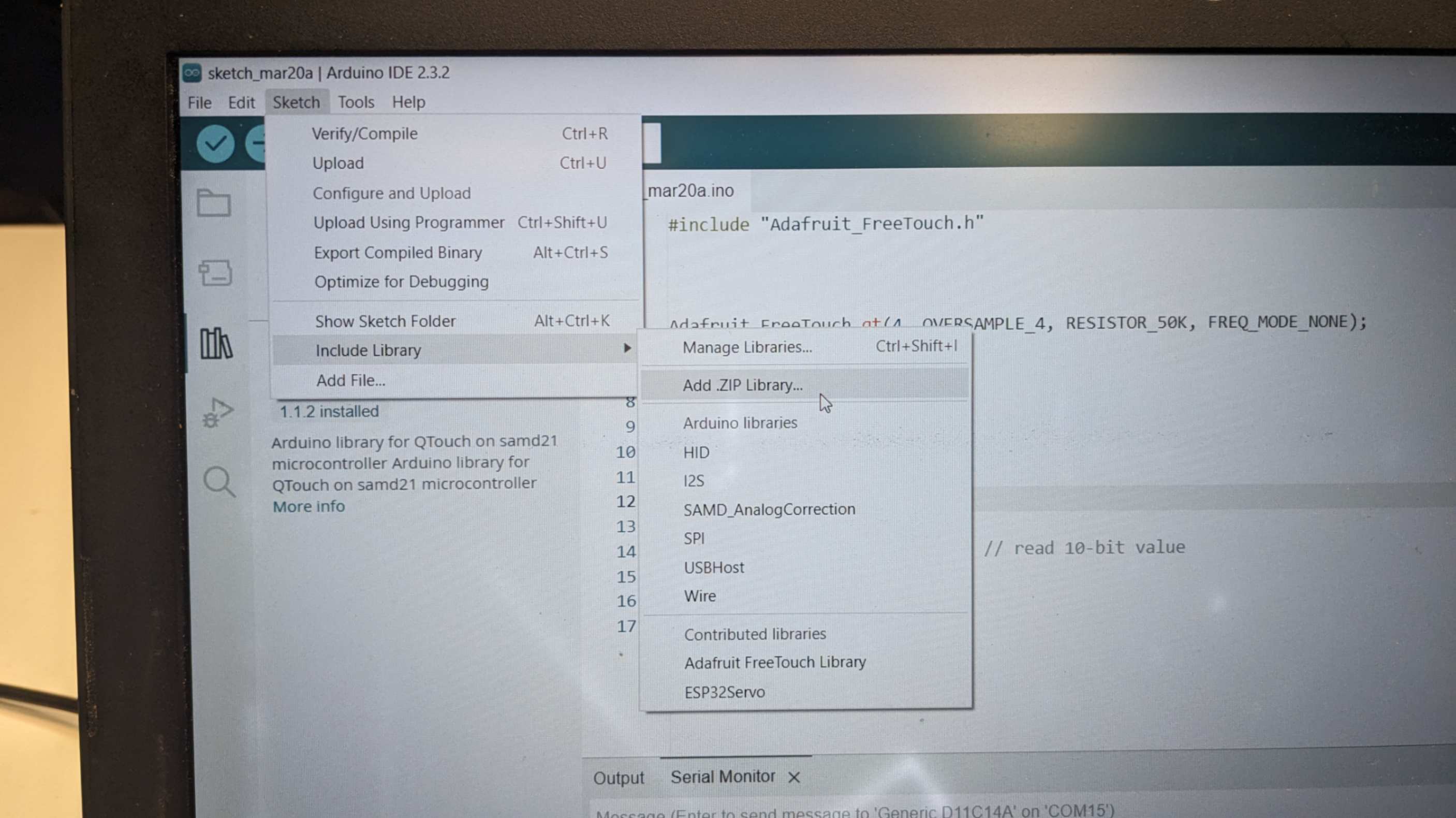
- Install the Adafruit Freetouch library from Adafuit_FreeTouch as Zip file
- Sketch tab - Include Library - Add Zip Library
- add the Freetouch Zip file
- Use the minimal example from Adafuit_FreeTouch
- Change TouchPad pin according to my boad
- Add, Serial.begin(115200);
- Add, Serial.printIn(qt_value);
- Add, delay(500);
- Upload the code
Video(.mp4)
W8_Touch the SAMD11_FA2024RY_compress.mp4
#include "Adafruit_FreeTouch.h"

                const int ledpin = 15;

                Adafruit_FreeTouch qt1(4, OVERSAMPLE_4, RESISTOR_50K, FREQ_MODE_NONE);
                Adafruit_FreeTouch qt2(2, OVERSAMPLE_4, RESISTOR_50K, FREQ_MODE_NONE);
                Adafruit_FreeTouch qt3(14, OVERSAMPLE_4, RESISTOR_50K, FREQ_MODE_NONE);

                void setup() {
                  qt1.begin();
                  qt2.begin();
                  qt3.begin();
                  Serial.begin(115200);
                  pinMode(ledpin,OUTPUT);
                }


                void loop() {

                  int qt1_value = qt1.measure(); // read 10-bit value
                  Serial.println(qt1_value);
                  delay(100);

                  if(qt1_value>500){
                    digitalWrite(ledpin, HIGH);
                  }
                   else{
                    digitalWrite(ledpin, LOW);
                  }

                  int qt2_value = qt2.measure(); // read 10-bit value
                  Serial.println(qt2_value);
                  delay(100);

                  if(qt2_value>500){
                    digitalWrite(ledpin, HIGH);
                    delay(100);
                    digitalWrite(ledpin,LOW);
                    delay(100);
                  }

                  int qt3_value = qt3.measure(); // read 10-bit value
                  Serial.println(qt3_value);
                  delay(100);

                  if(qt3_value>500){
                    digitalWrite(ledpin, HIGH);
                    delay(10);
                    digitalWrite(ledpin,LOW);
                    delay(10);
                  }

                }