2-layer PCB Manufacturing
As I was designing the circuit board, it quickly became clear that I would need to use a double-sided board. There are just too many wires that need to cross over each other, if I used 0-ohm "jumper" resistors instead I'd need like 50-100 of them. I've been wanting to learn how to make a 2-layer board for a while, so I developed techniques for doing that in my final project. I'll explain my approach in detail here, since it might be useful to other people:
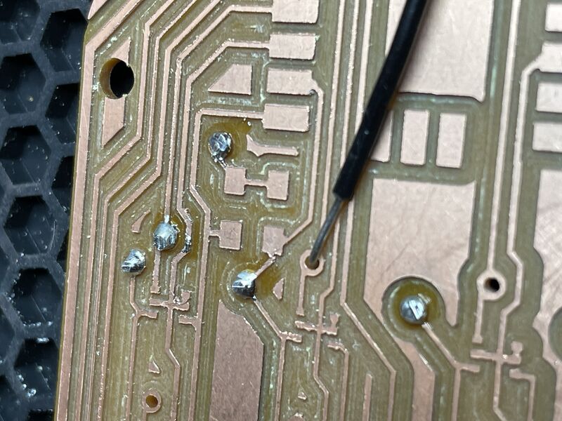
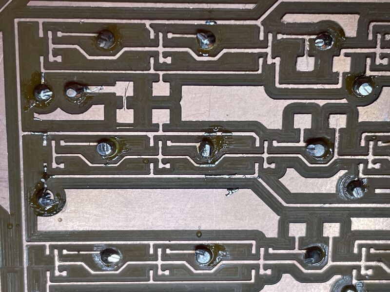
"Vias" are small holes filled with conductive metal that carry the signals from one side of the board to the other. Commercial boards usually plate the inside of these holes with gold. For prototyping, you can get PCB via rivets.. Instead, I hand-soldered little pieces of wire through the holes.
Design
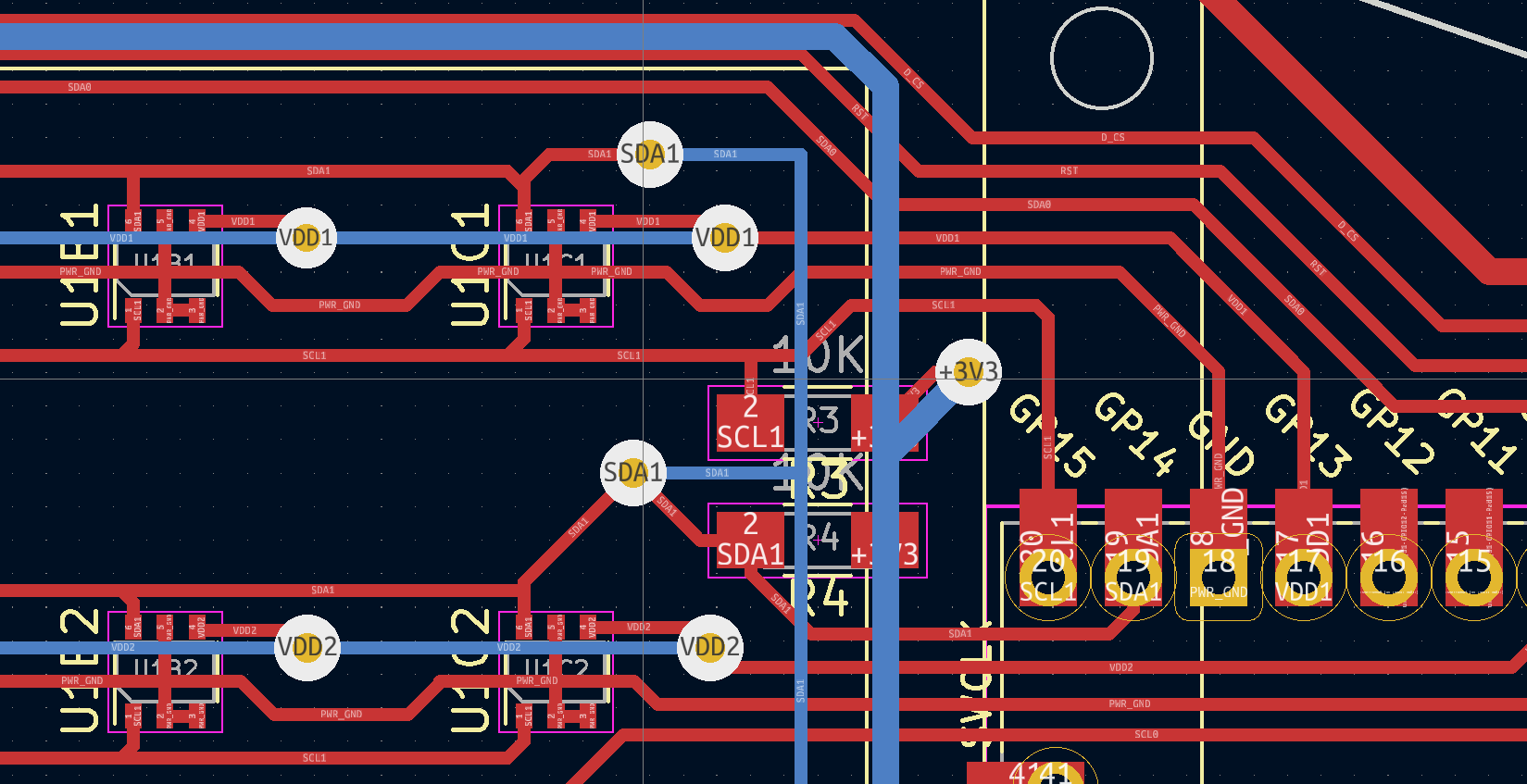
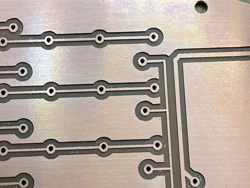
In designing the board, I made sure my vias were large enough to be drilled using a 0.8 mm endmill, and soldered by hand. This means they must be much larger than the KiCAD default size. I made the holes 0.9 mm in diameter, with a 2 mm diameter solder pad around that. In KiCAD, you can hit the page up / page down keys while drawing traces to switch from the top to the bottom layer, adding a via automatically.
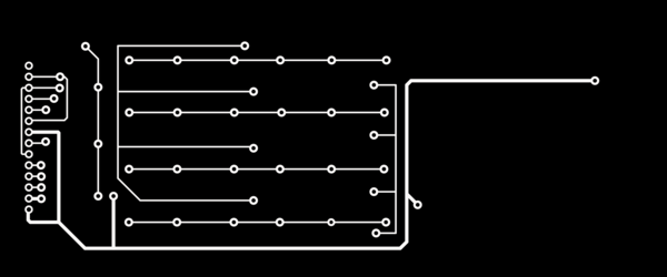
As part of the design, I included four 3-mm screw holes. These will help to hold the project together once it's built, but they're crucial when making a 2-layer board since they act as alignment holes. You've got to make sure the bottom layers is exactly lined up with the top! In manufacturing, these alignment holes will fit over matching pegs fitted into the spoilboard of the CNC. Yes you will be making holes in your CNC table to do this.
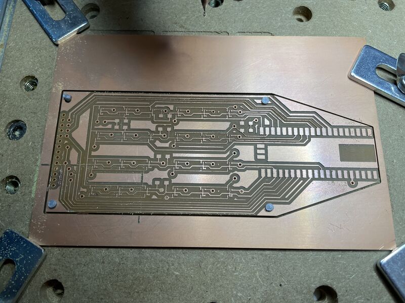
As I designed my board, I put all components, and as many traces as possible, on the top layer. That way, if the two-layer PCB process didn't work, I could replace the traces on the bottom with hand-soldered wires.
CAM preparation
I prepared the design for manufacturing using KiCAD, Adobe Illustrator, and MODS. I exported the top, bottom, and edge_cuts layers from KiCAD as SVG files. In Illustrator, I stacked these files as separate layers. I then reorganized the components into the new layers below and exported as PNG. The layers were then brought into MODS, and milled using the following settings for each:


Milling
It is absolutely vital that the milling machine's X,Y zero position stay the same for all of these steps!
Milling steps proceeded in the order listed above. First, I cut the alignment holes using a 1.5 mm endmill. I had to use a big mill to make a 9 mm deep cut into the spoilboard. I inserted alignment pegs through the PCB and into the spoilboard. Since 3mm screws are slightly smaller than 3 mm, I 3-d printed plastic alignment pegs. These can be made exactly the right size to get a nice snug fit, and since they're made of plastic they're less likely to break the endmills if there's an unexpected crash.
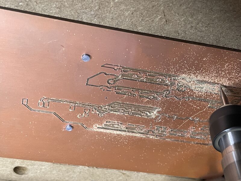
Machining the rest of the front of the board proceeded as normal. Then I removed the board and flipped it over, realigning it with the pegs. I made sure to flip the board the same way I mirrored the image in the preparation step! (Top-to-bottom rather than left-to-right, in my case.) Next I milled the back-side traces.
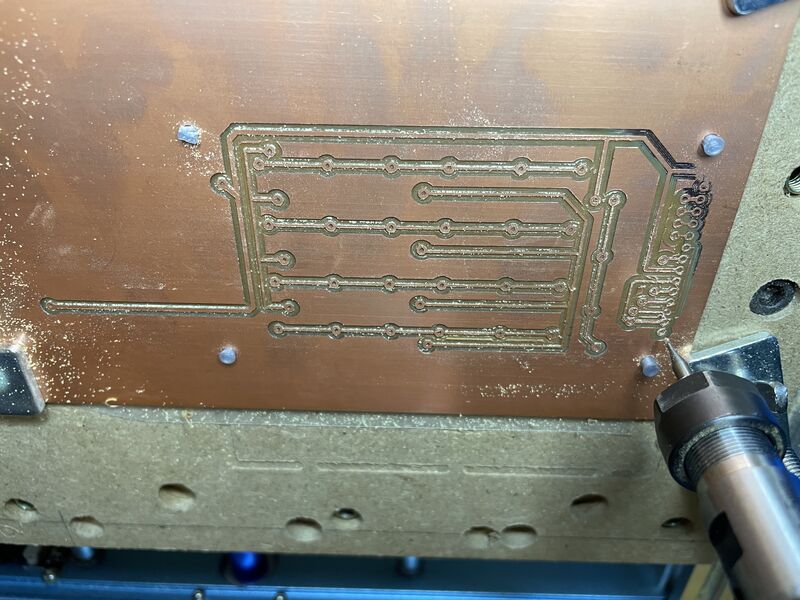
Finally, the through holes, vias, and board outline need to be cut. A clever person might flip these in Illustrator so they can be machined from the back of the board, but I didn't do that, so I flipped the board back to the front side again to finish the milling process.
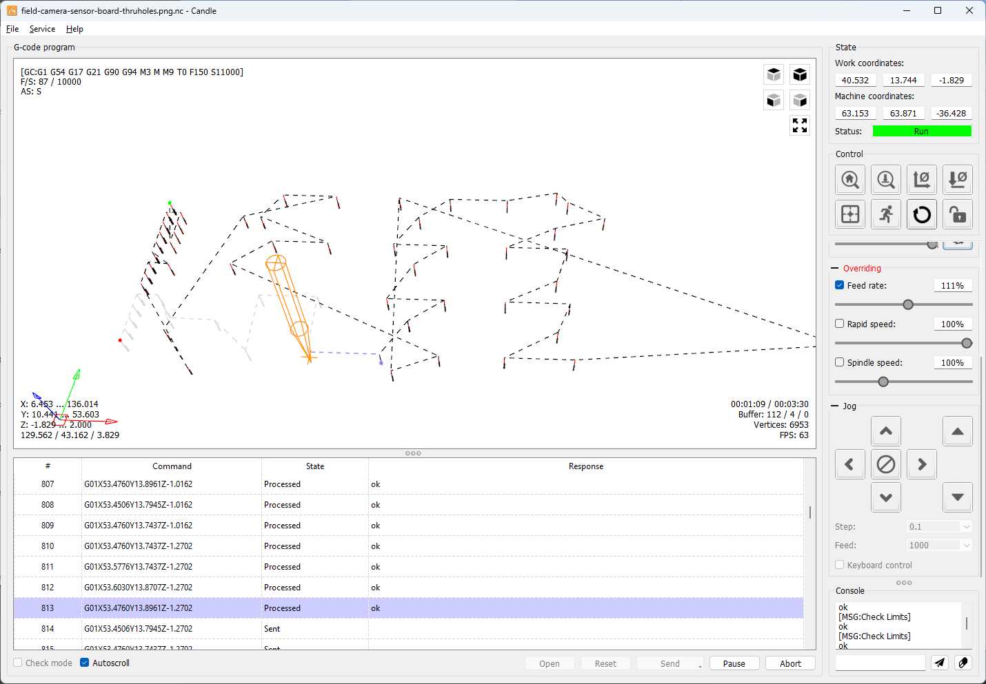
You'll know it worked if the via through holes line up perfectly with the pads on the back side. In my case, the deviation was just barely visible.
Soldering
To make the connection from the front of the board to the back, small pieces of wire need to be soldered into the holes. Here's my process for doing that:- I soldered the vias first. I used high-temperature wire solder, not paste, to make sure the vias don't melt while soldering other components later on.
- I stripped the insulation from a short length of 22-gauge solid core hookup wire, and bent a small "L" in the end.
- I inserted the little "L" into the via hole so it stuck out the back a few mm, and soldered it on the front side.
- Then I flipped the board over and soldered the other side.
- Finally I cut the wire and solder close to the board with flush cutters on both sides. I learned the hard way that you have to do this last! If you cut the wire short before soldering the back, the capillary action from the solder will pull the little stub of wire right out of the hole!

Avoiding Mistakes
Since replacing this board would be a lot of work, I used extreme caution when assembling it. I took the following precautions:- I soldered all the wiring and passive components first, and tested all connections with a multimeter before adding anything difficult to replace.
- I re-tested for continuity after adding each magnetometer chip. Since so many chips share a single net, this is the only way to figure out which one of them is short-circuited. People say you can just stuff the whole board and solder it all at once, but IMO that's a recipe for disaster.
- Most important: I did not solder the LCD panel on permanently, as designed. I used an 0.1" socket header so that it is removable. This increases the spacing between magnetometers and screen, but allows me to fix problems with the PCB without unsoldering the screen. And it's a good thing I did!
Fixing Mistakes and Problems
I made at least three errors while building this, despite my precautions.- The board was upside-down in my head when I first started, so I soldered the first magnetometer on upside-down. When that failed the continuity test (it has internally connected ground pins), I tried soldering it in a fresh spot, multiple times, before realizing my mistake. As a result this row of pads isn't as clean as it could be.
- I ripped two short traces leading to one of the magnetometers. I repaired them by soldering strands of fine wire in their place.
- This one's not my fault: it turns out the specific LCD driver I'm using for this project, the ILI9488, has a bug: its MISO pin doesn't cooperate with other devices on the same SPI network. Fortunately since the screen doesn't need to talk back to the processor, it doesn't need a MISO pin. So I cut the trace on the PCB, so that the processor's MISO pin connects only to the touchscreen. (I would never have solved this if it weren't for helpful comments in Bodmer's eTFT_SPI library)!