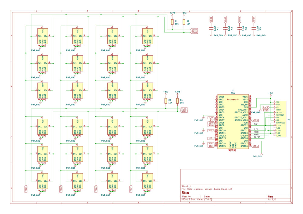
As discussed in the Components page, I decided on the following scheme to control as many sensors as possible:
- Use the 2 hardware I2C interfaces built into the RP2040
- Use the 3 different sensor models sold by the manufacturer, which have different default I2C addresses
- Use 4 copies of each model on each interface, reprogramming them to have unique I2C addresses.
- ================================
- For a total of 24 individual sensors.
I will reprogram the I2C addresses by sequentially powering on a bank of chips, assigning their I2C addresses, then turning on the next bank of chips. In my design, I I have labeled the sensors: "U1A3" refers to the sensor on I2C interface #1, chip model A, power bank 3. Here's a layout of how the system will work:

 Routing traces for the board was quite difficult, given the complexity of the circuit. I was forced to make two design compromises to get the routing to work:
- I had to rotate the RP2040 so it sticks out sideways from the sensor array. Thus the final design will have a "handle" containing the processor, so it won't just look like a cell phone or tablet.
- I had to commit to making a 2-layer PCB design. This is significantly more complex than a 1-layer board, but the alternative would have involved 50-100 zero-ohm jumper resistors! In my previous experience, routing traces under jumper resistors is just asking for soldering problems.
My final board layout looks like this:
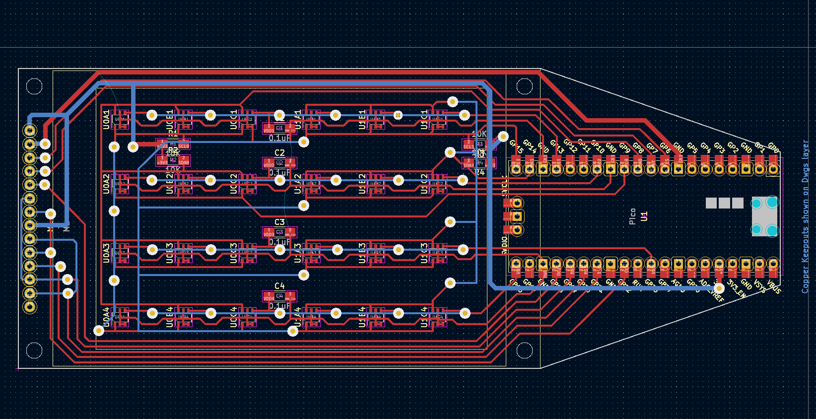 Here it is with some layout annotation:
 It has about 48 vias. Yikes. Hopefully that won't be too bad to solder.
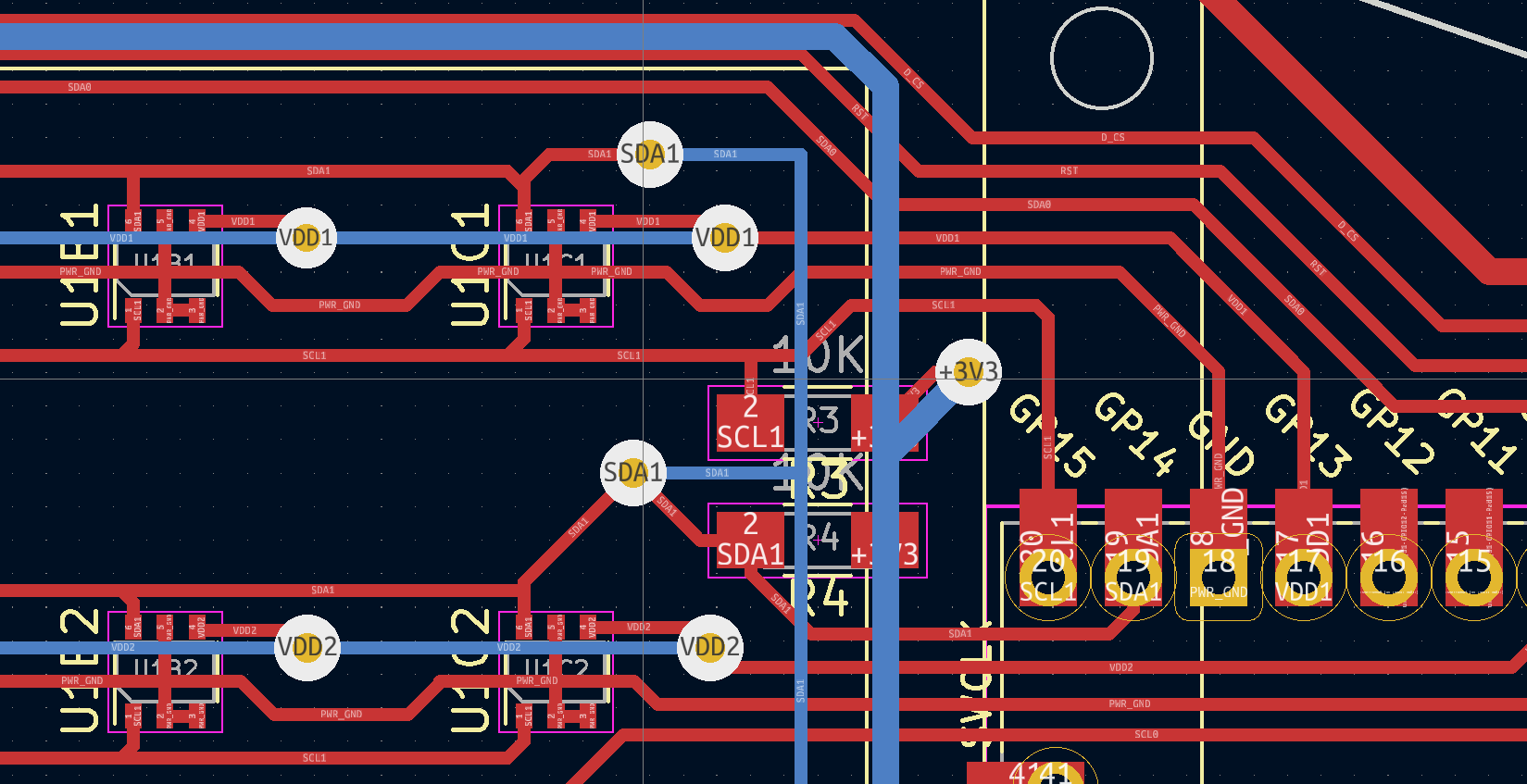
Here's a close-up of some of the details of the final board design: