Week 6: Electronics design
This week I designed a development board for a Xiao ESP32 C3 microcontroller.
I also worked in a group to learn how to use an oscilloscope and a multimeter. The group documentation can be found here.
Group work
The oscilloscope was entirely new to me, and very interesting. I'm sure at some point I may want to use one for debugging. I learned how to use some settings on the multimeter I hadn't used before.
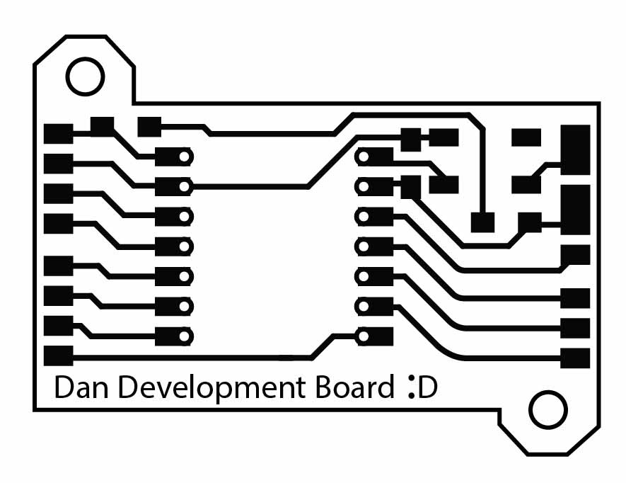
Xiao ESP32 C3 development board
Kicad files .zip (download)
Board svg (download)
I made a development board with plug-in connections for all of the pins on the ESP32.
I started by installing Kicad and the Fab part library.
To install the Fab part library:
1: Clone this repository to a folder on your computer: git@gitlab.fabcloud.org:pub/libraries/electronics/kicad.git
2: One of the cloned folders should be titled "KiCad". move this to a safe location. I recomend making a library folder in documents/KiCad/7.0 and renaming the KiCad folder to Fab so you will recognise it when looking for the fab component library in KiCad.
3: Open Kicad and then preferences - manage symbol libraries. Then hit the rocomended option if a pop up comes up.
4: Click the + at the bottom left of the symbol libraries panel to create a new row.
5: Click in the cell for the “Library Path”, then select the folder icon, then select “fab.kicad_sym” from the repo you cloned. If will be easier to find if you nickname it Fab.
6: Now go to preferences - manage footprint libraries, then again hit the recomended option if the pop up shows.
7: Click the +, and this time in the library path select the entire Fab.pretty folder, nickname it Fab if you like, and hit ok.
8: finally go to preferences - configure paths, and hit the + to add a new path that points to the entire folder you cloned. You can set the variable name to Fab.
Kicad
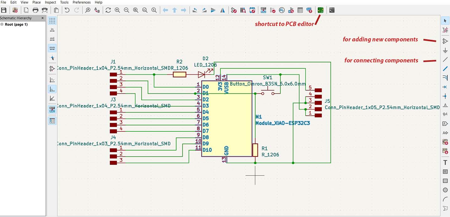
Once in Kicad, I added in all of the parts I would need for my board. This included the ESP32 itself, a resistor, an Led, and some horizontal pins. Later I added a button and a pull-down resistor. I used the wire tool to connect everything together. I decided on the horizontal pin numbers with the shape of the ESP32 in mind. I wanted a port for every pin on the ESP32 and an extra for ground and 5V. I also wanted my board to be reasonably compact and have an even number of pins on each side.
PCB Editor
With the connections done, I switched over to the PCB editor to make the wire trace layout. I made it on two separate layers by accident, but this didn’t end up causing any problems so I didn’t fix it. In order to keep my design compact and prevent unwanted contact, I routed some of the wires under the button and resistors. I planned on soldering a battery connection onto the bottom of the board, which will require elevating the board with vertical pin connections. This meant that I could easily rout wires underneath the ESP32 itself. On the image to the right I have pointed out a couple of important buttons for making a board such as this. You should also note the dropdown in the top left corner of the screen, where you can change the width of the wire traces. For the mill I was working with, a trace width of 0.5mm was good. There is also a dropdown where you can change the precision of the grid with which you can place the traces in your design.
DRC
I ran the DRC tests and found that it wanted an outline for the board and it was confused by the two separate layers. I decided neither of these warnings were problematic as I could fix them in Illustrator.
Adobe Illustrator
Once I was Happy with the layout, I exported the 2 layers as SVGs, and opened them in Adobe Illustrator. I combined them into one document and overlapped them.
Finally I made an outline and added some text to finish it off. I added a couple of screw holes for easy mounting.
I kept the traces, holes, and outline on seperate layers in Illustrator. This is important because these will be seperate operations when it comes time to mill the board.


