This week, I worked with my group on learning how to use a multimeter to measure voltage, current, and resistance. We also learned how to use an oscilloscope to measure and graph voltage. Here is a link to the complete process. For my individual assignment, I designed a development board in KiCad.
6. Electronics Design
Schematic
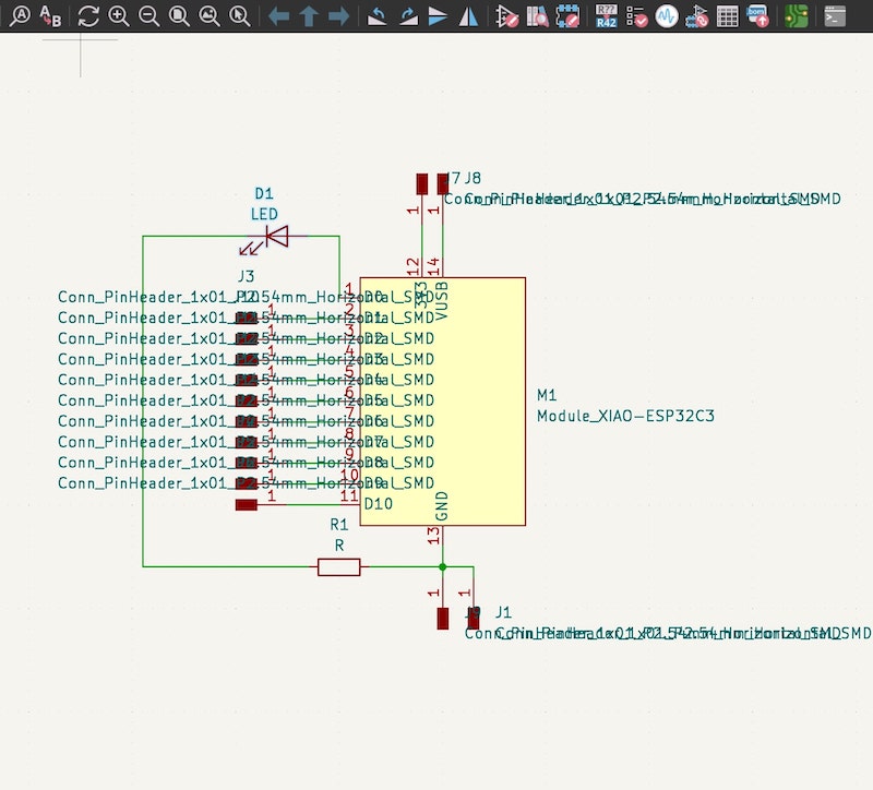
On KiCad, I created a new project that automatically created shematic and PCB files for me. To start, I opened the schematic file and using the Add A Symbol tool on the right bar, I searched for ESP323C in the fab library I had already installed following these instructions and added it to my schematic. Then, I added surface-mounted pin headers and connected them to the ESP32 pins. I also added an LED and a resistor to incorporate them with my board. I connected the LED and resistor to pin D0 and GND. I had my complete schematic shown in the screenshot on the right.
ERC
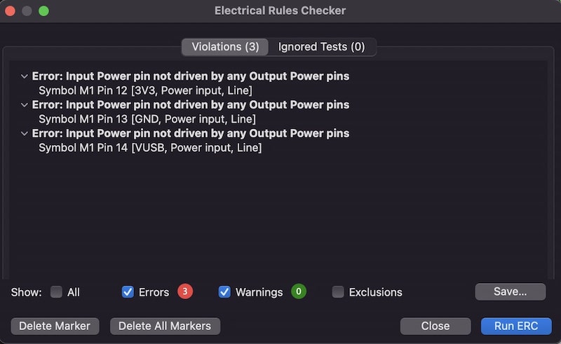
Then, I had to run the Electric Rules Check(ERC) to check if any electric connection was wrong. I received three errors saying that the input pins were not driven by output pins. This was not true though as all input pins were connected to output pins. So I decied to ignore the errors.
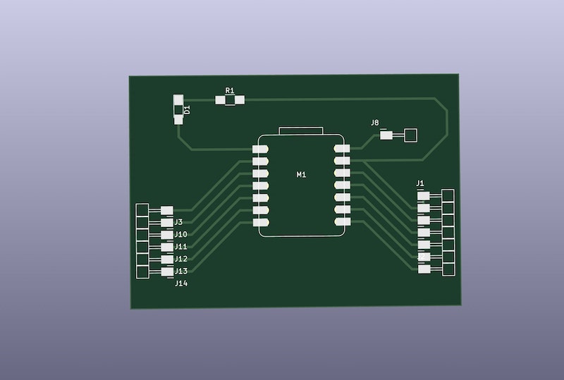
PCB Design
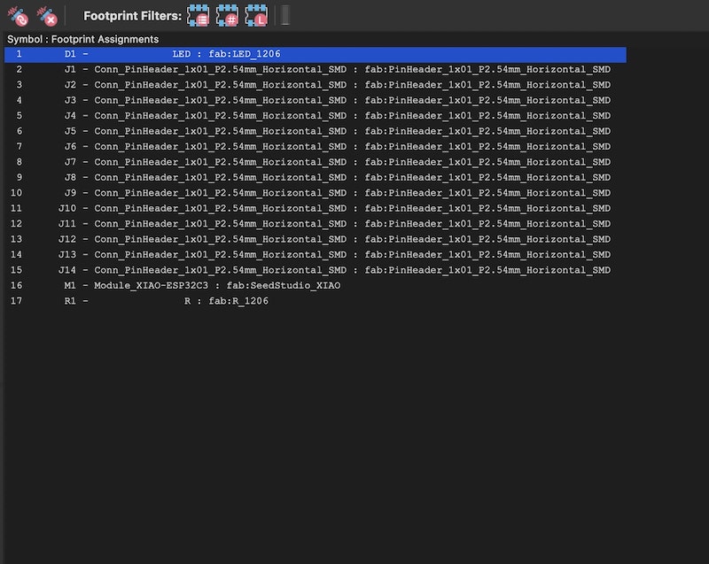
The next step was the PCB design. First, I needed to assign Footprints to my Symbols. I clicked on Tools/Assign Footprints and found that the pin headers and the ESP board were assigned footprints by default as there is only one footprint for each. I just had to choose for the LED and the resistor. I chose surface-mounted LED and resistor as they are smaller and look better on the board than through-hole ones.
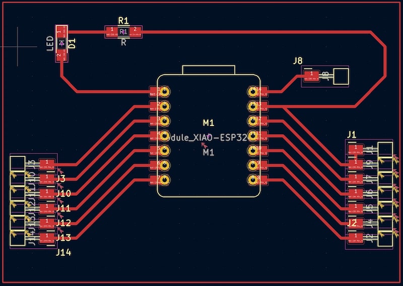
Next, I clicked on Tools/Update PCB from Schematic which opened the PCB design page. I organized the components and drew the traces. However, I had to increase the width of the traces from 0.25 mm(default) to 0.5 mm to make it easier for the machine to mill them. To do that I clicked on Track/Edit Pre-defined Sizes on the top left and created a new size. Finally, I drew the outline using the rectangle tool on the right bar. My PCB design looks like this.
DRC
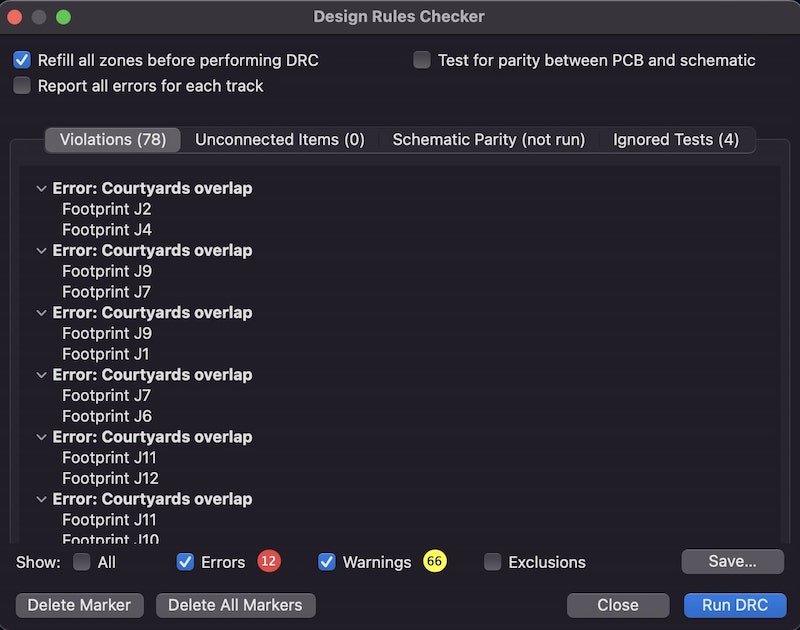
Finally, I run the Design Rules Check(DRC) to find out if my design was compoatiblw with KICad Design Rules. The only error I receiced was courtyards overlap. However, the spacing between the pins was consistent with the spacing between the actual pins I wanted to solder on the board. I think the error was because I used individual pin headers instaed of a set of 6, but there is no acual influence on the design and milling. So I decided to ignore the error.