Week12: networking and communication
Group assignment:
Send a message between two projects
Individual assignment:
Design, build, and connect wired or wireless node(s) with network or bus addresses.
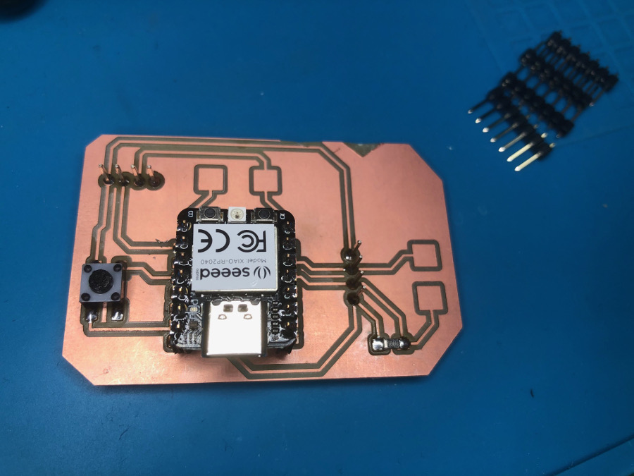
For the assignment, I have created a PCB with one module XIAO-RP2040 that will be leveraged to create a serial connection between 2 identical PCBs.
2 PCBs will be produced (identical ones) and with these 2 PCBs, I will be in a position to test two different protocols
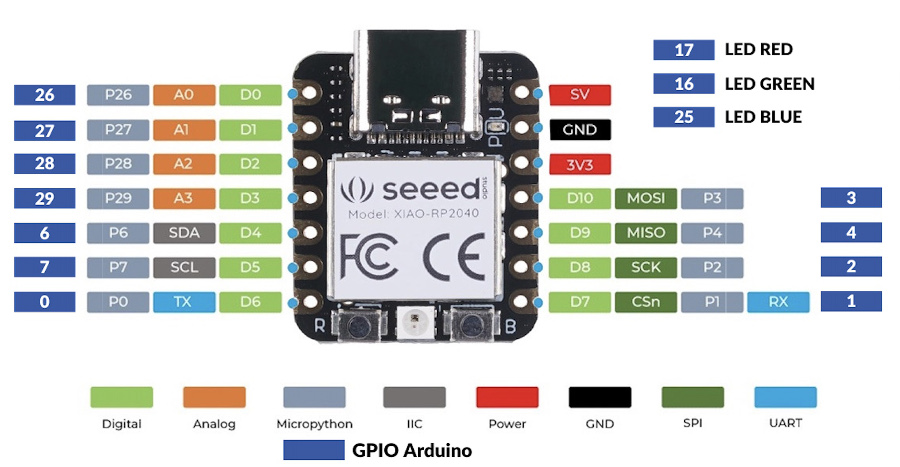
Refresh on the Module_XIAO-RP2040 PINs:
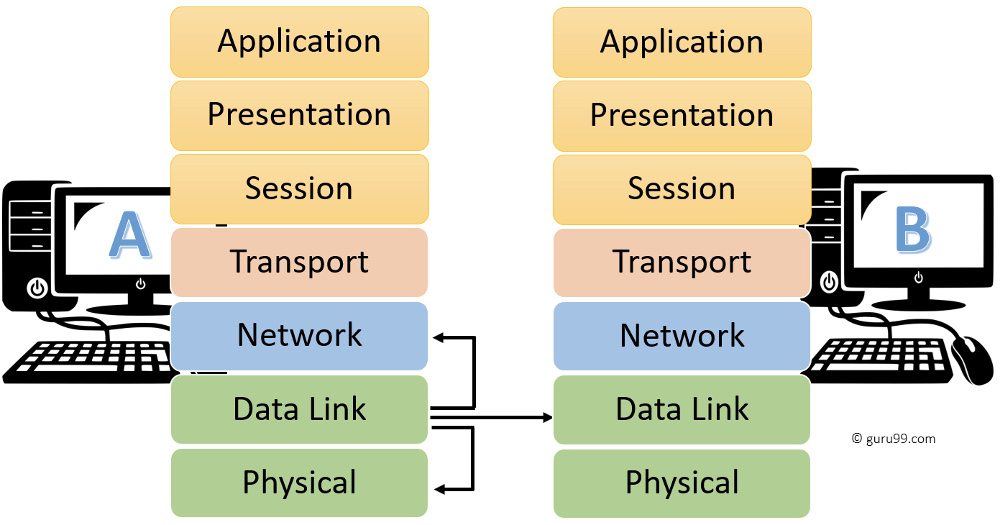
2C (Inter-Integrated Circuit) is a communication protocol that allows multiple digital components to communicate with each other using only two wires. The protocol was developed by Philips Semiconductors (now NXP Semiconductors) in the 1980s and has become a standard for communication between various electronic devices.
I2C protocol uses a master-slave architecture where the master device initiates the communication and the slave device responds to the master's commands. The two wires used for communicationare a serial data line (SDA) and a serial clock line (SCL). The master device generates the clock signal, and the slave device synchronizes its data transfer to this clock signal.
I2C protocol supports multi-master communication, which means that multiple master devices can communicate with multiple slave devices. The protocol also supports different data rates, and the data transfer can be done in either direction.
I2C protocol is widely used in various applications, such as sensors, EEPROMs, RTCs, and other embedded systems. It is a simple and efficient communication protocol that allows foreasy integration of different digital components in electronic systems.
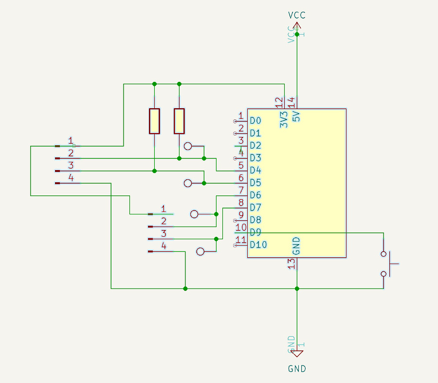
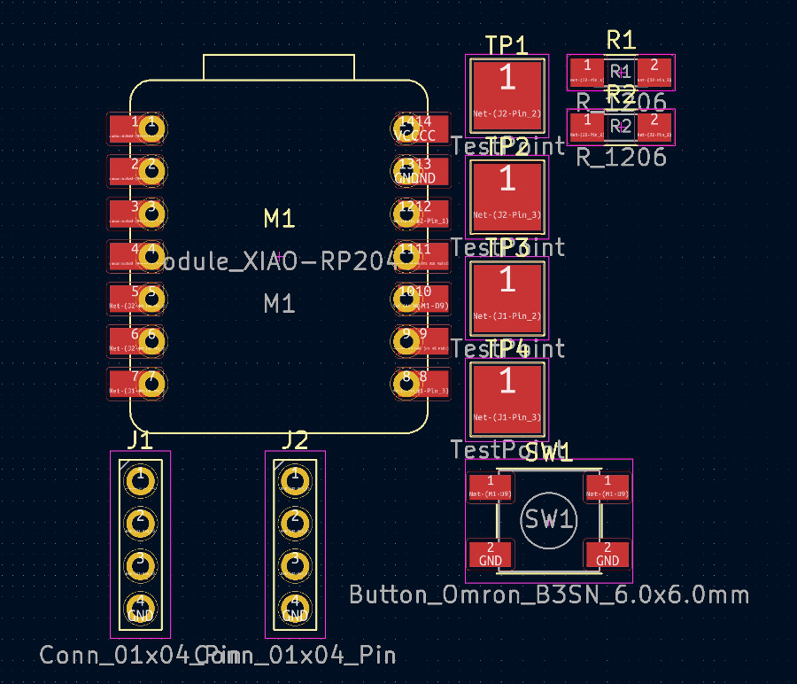
Let's design one PCB to enable the testing of serial and I2C protocol, by adding the following list of components:
PCB schematics creation
Creation of the schematics using Kicad.Overview of the schematic when completed:
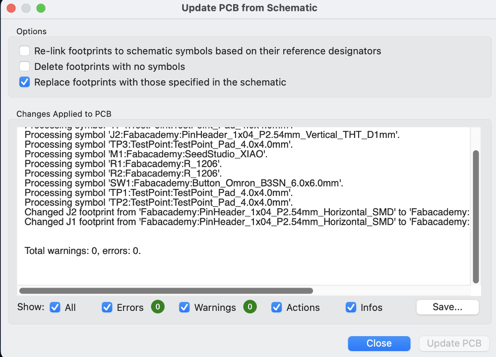
Then the footprints have been assigned to the electronic components:
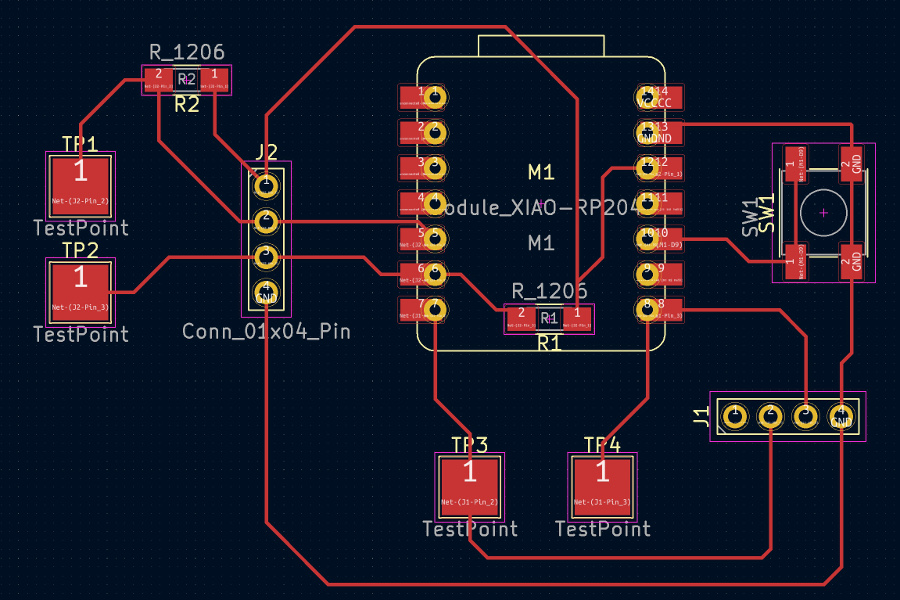
At completion of this assignment process, the following preview is available:
Then I started the move of the electronic components to remove all tracks crosses and I completed the routing.
Overview of the project at completioon of these two taks:
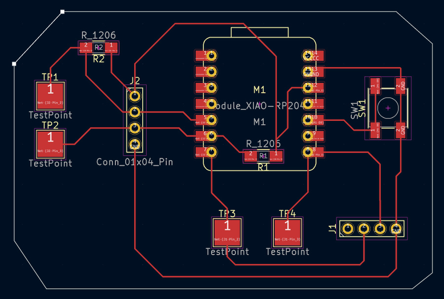
Then I created the edges of the PCB:
KiCad project file download
Last step of the activities on Kicad consist, as usual, in the creation of two .svg files: one for the wires and one for the outlines
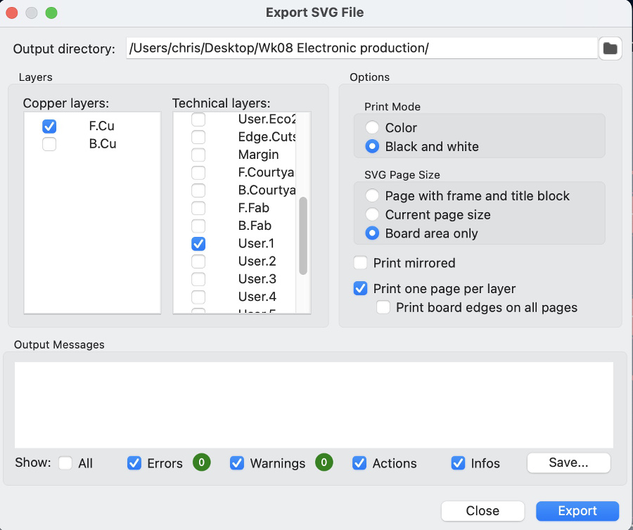
These files can be found here:
After that, I have created an additional .svg file for the "holes layout" using Inkscape software.
.rml files generation
Leveraging the Modsproject online platform to create the 3 .rml files (wires, holes, outline):
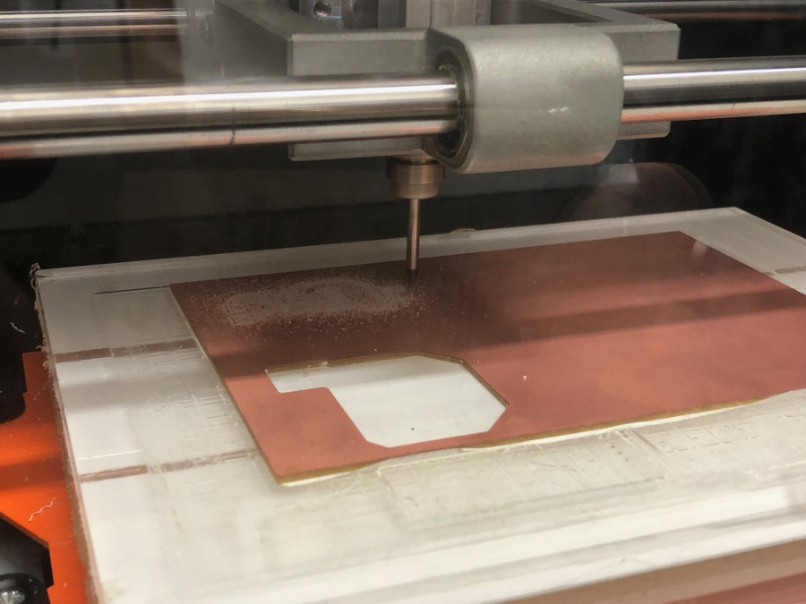
Milling of the 2 PCBs
Start of the milling activities on the Roland SRM-20 machine: step1 - wires
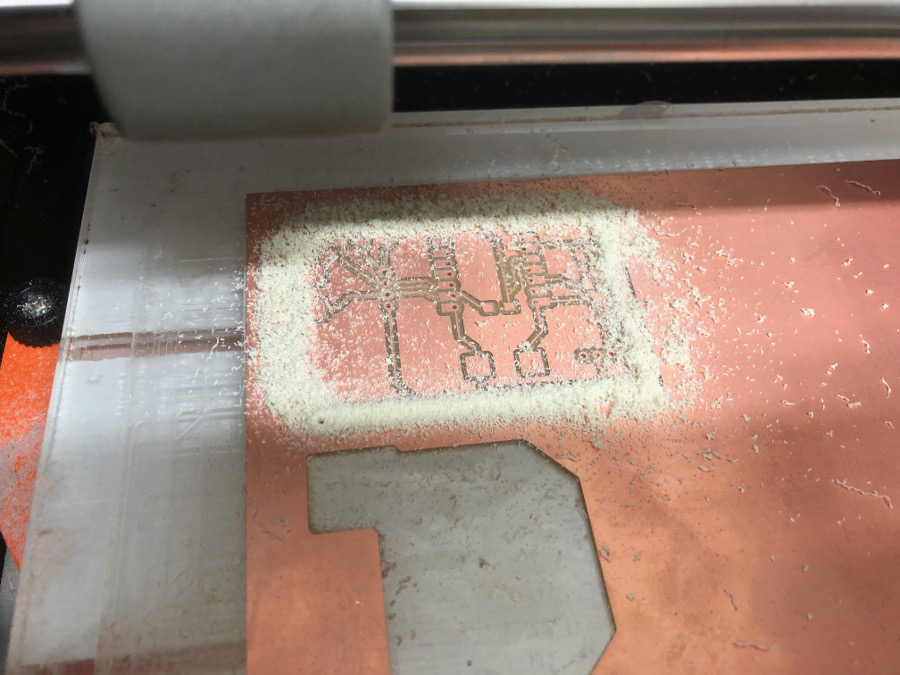
Overview of the PCB right after completion of the whole milling process (step1: Wires => step2: holes => step3: outlines)
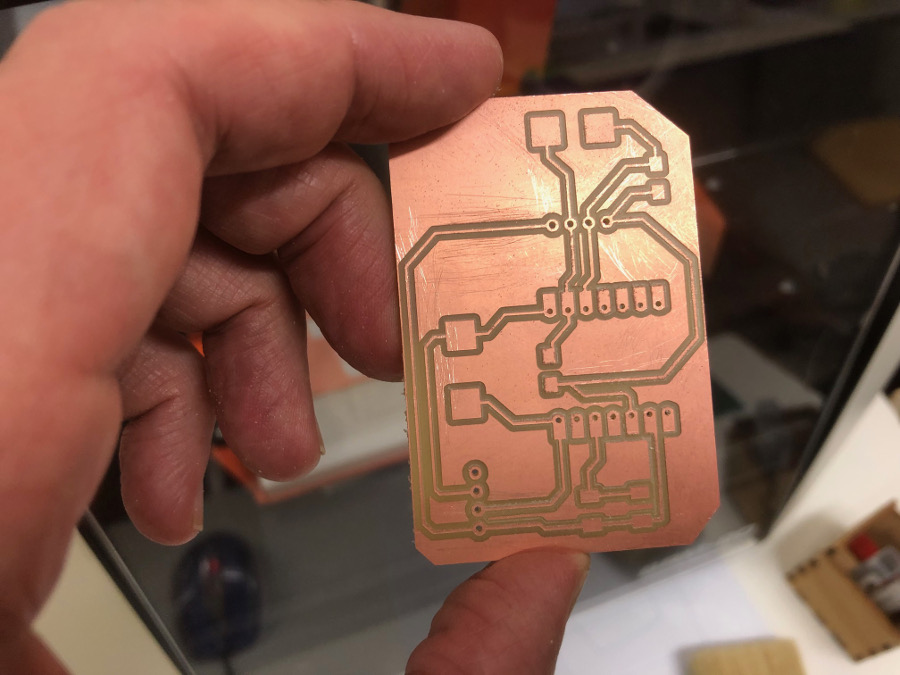
Overview of the PCB after clean-up with tepid water and dried with a tissue paper.
The pcb at first glance looks pretty ok but I decided to gently pass fine grit sandpaper over the card. You can see the scratches left by the passage of the glass paper on the wires of the PCB. in this way, it should be perfect.
Soldering of the components on the 2 PCBs
It took approximately 1hour 15 minutes to complete the soldering activities for the 2 PCBs.
Activities have been produced in full respect of the safety and security rules, use of a fume extractor..
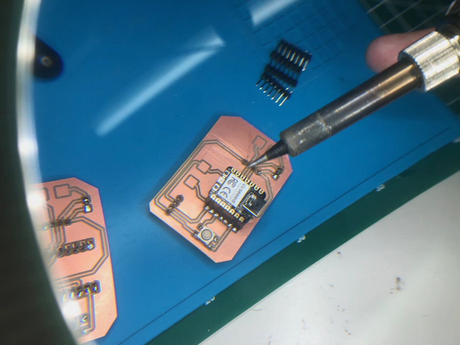
Snapshot of the first PCB at completion of soldering activities:
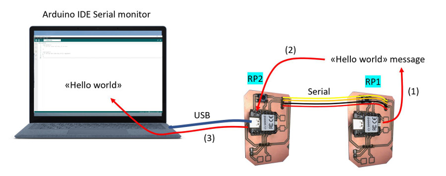
Networking and communication test design
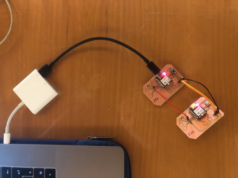
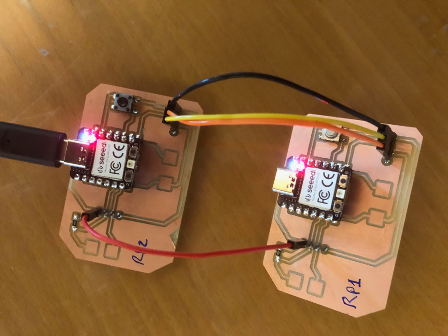
Idea is to run a test using the serial protocol between the two PCBs created (RP1 and RP2)
RP2 will be connected to the USB port of my laptop and RP1 and RP2 will communicate through a serial protocol
The test will consist in the following:
Tests execution:
Preliminary test #1:
The first test I did was to create a simple sketch with Arduino IDE where the BLUE LED of the XIAO RP2040 will blink for on second and then will be switched off for one second
This test has been executed for each Module_XIAO-RP2040 disconnected from he PCB first and then connected to the PCB
All tests related to the preliminary test #1 where at this stage successfull.
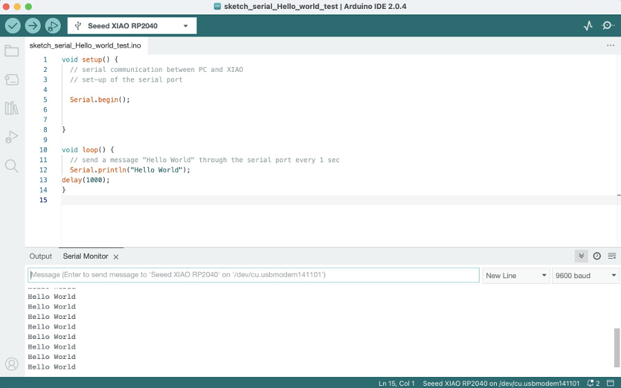
Preliminary test #2:
For this test, we will set-up a serial communication between the laptop and the XIAO-RP2040.
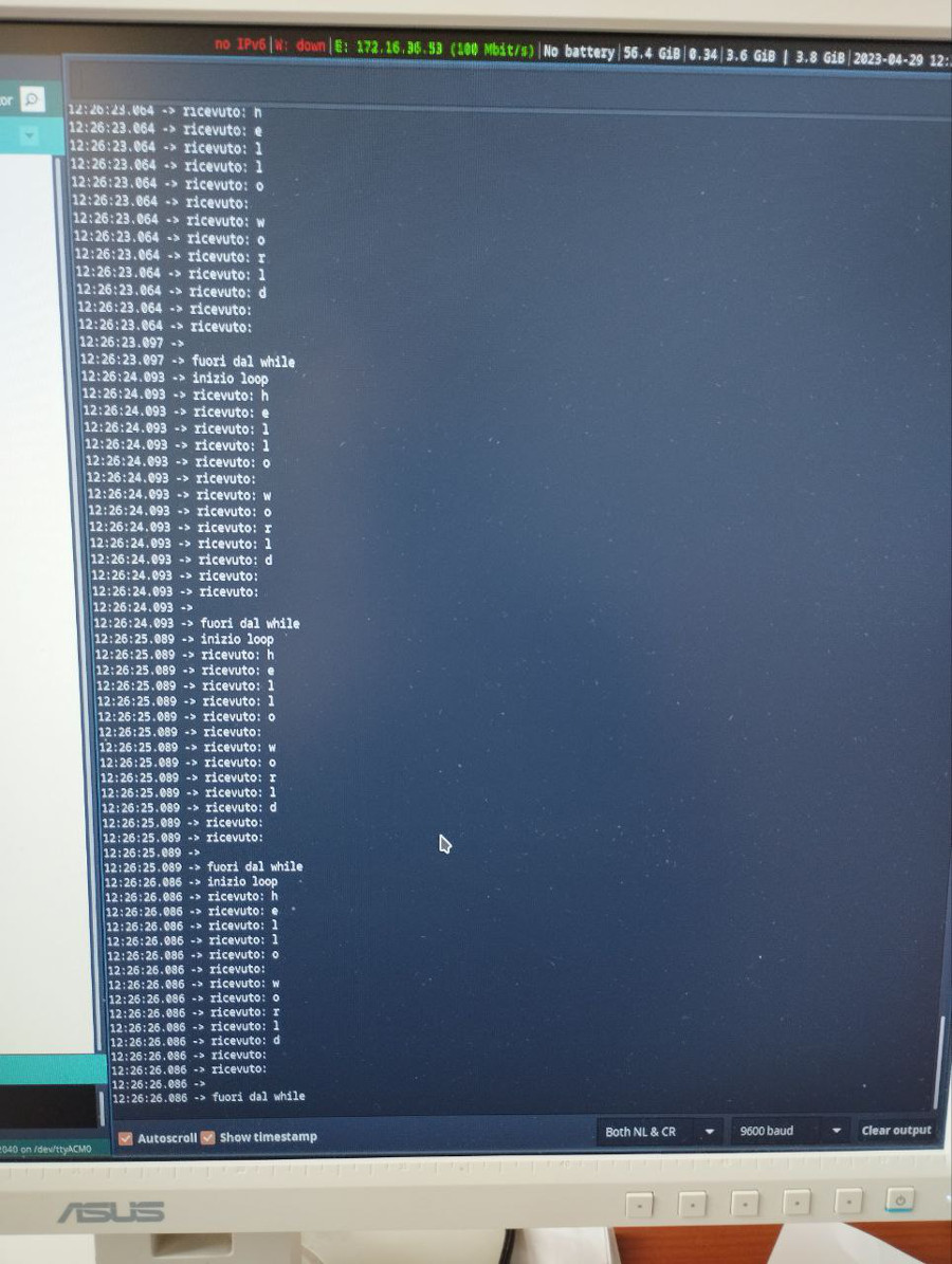
As soon as the communication is established through the serial port (Serial.begin), the XIAO-RP2040 will start sending every second a "Hello World" message that will be visualized on the serial monitor of the Arduino IDE.
As per image below, the preliminary test #2 has been executed successfully on the RP1 and then on the RP2.
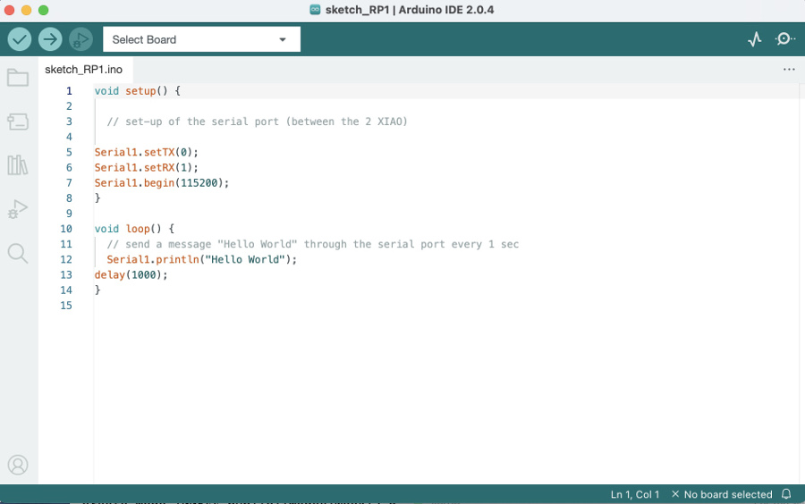
Sketch on RP1
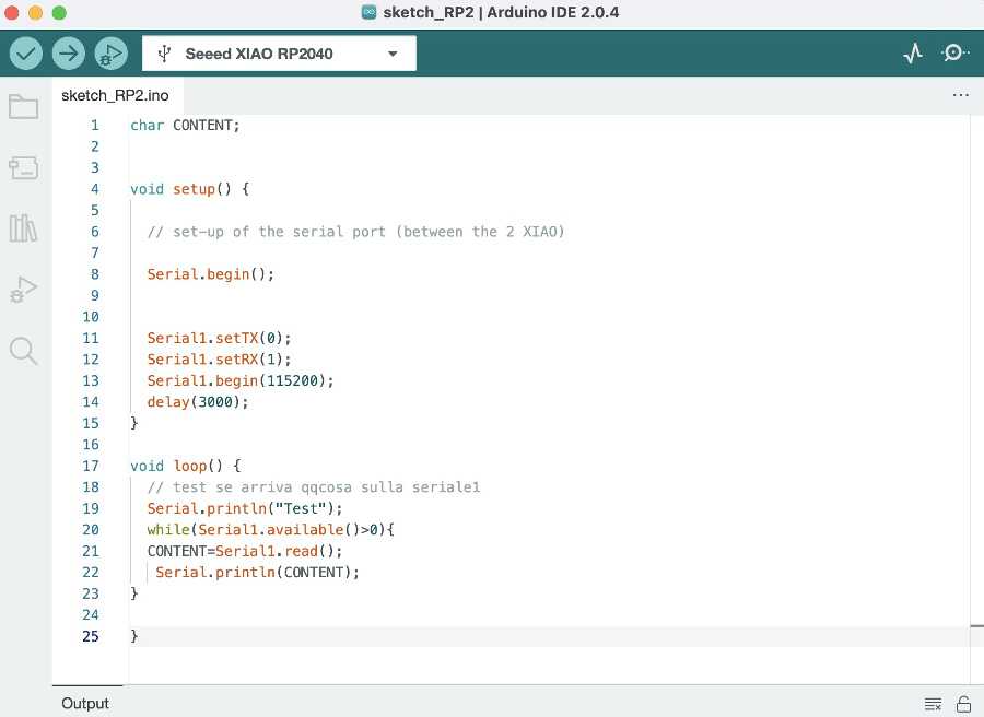
Sketch on RP2
The first test "End2End was not successfull and required some troubleshooting.
The code on RP1 has been modified and adding a certain delay before starting RP1, to allow RP2 to correctly initialize its serial ports before being hit by data coming from from RP1.
After implementation of this change, End2End flow started to work correctly.
Overview of the serial monitor which shows the reception of the message "hello world" byte by byte. Note: after the letter "d", we observe the reception of 2 "empty" bytes. These 2 empty bytes correspond to the symbol "carriage return" (\r) and to the symbol "newline" (\n), that the Serial.println command (used in the RP1 code) automatically put in the queue of the messages it sends.
 RP1 Code
RP2 Code
RP1 Code
RP2 Code