Week09. Output device.
Types of output devices:
Output devices in electronic systems transform electrical energy into another type of energy, such as light, sound or kinetic energy
MOSFET concept:
The MOSFET (Metal–Oxide–Semiconductor-Field-Effect-Transistor is one of the most common type of transistor today. They are primarily used to control conductivity (i.e how much electricity can flow) between its source and drain terminals based on the amount of voltage applied to its gate terminal.
Some output devices like motors, stepper motors can easily require 9V to 12V Voltage and currents in the range of 1A.These voltages and currents are not compatible with the micro-controllers that we use in our FabAcademy projects (max 100mA per PIN). For this consumptions reasons, the energy source need to be taken be sourced anymore by one PIN and need to be supplied elsewhere.
MOFSET and BJT(Bipolar Junction Transistor) are tripolar electronic components that offer great solutions to solve these challenges.
Note: MOFSET are more frequently used compared to BJT.
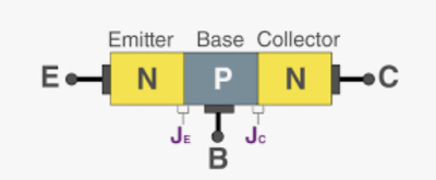
The BJT is also a tripolar component and works in a slightly different way compared to the MOSFET.
BJT can handle currents greater than 7A up to 20A and are mainly used in the field of analogical electronics
Small MOFSETs (without heat dissipation) can manage up to 3A and bigger MOSFETs can manage up to 7A
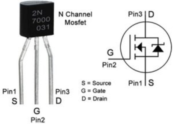
One good example of MOSFET frequently used in FabAcademy is the MOSFET SOT 23. It's a pretty tiny components.
The three poles of the MOSFET are:

Another MOSFET that we also have in our lab is the FDN337N
Related datasheet: https://www.farnell.com/datasheets/2304556.pdf
Let's open the datasheet and have a look at the top most important parameters to check when you are still in the design phase of your PCB:
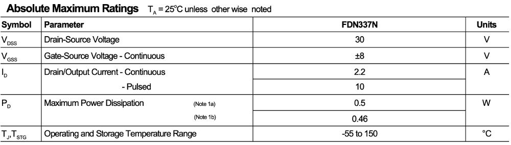
Other important parameter to monitor: VGS(th):

In this case, there is a need of at list 1V on the PIN to make the MOSFET work correctly. Since we have 3.3 V on the PIN, we are in the rights conditions to operate the MOSFET
Assignments
Group assignment:
To be completed
Individual assignment:
This week, I have been testing the Flexinol(R) acting as an output device / special actuator
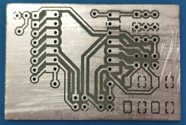
Step1: creation of a generic PCB that is expandable to support the testing activities of the Flexinol
This PCB includes:
The ide behind this PCB is that all the pins of the XIAO will be exposed via pinheader to enable the attachment of any expansion we may need for future experiments.
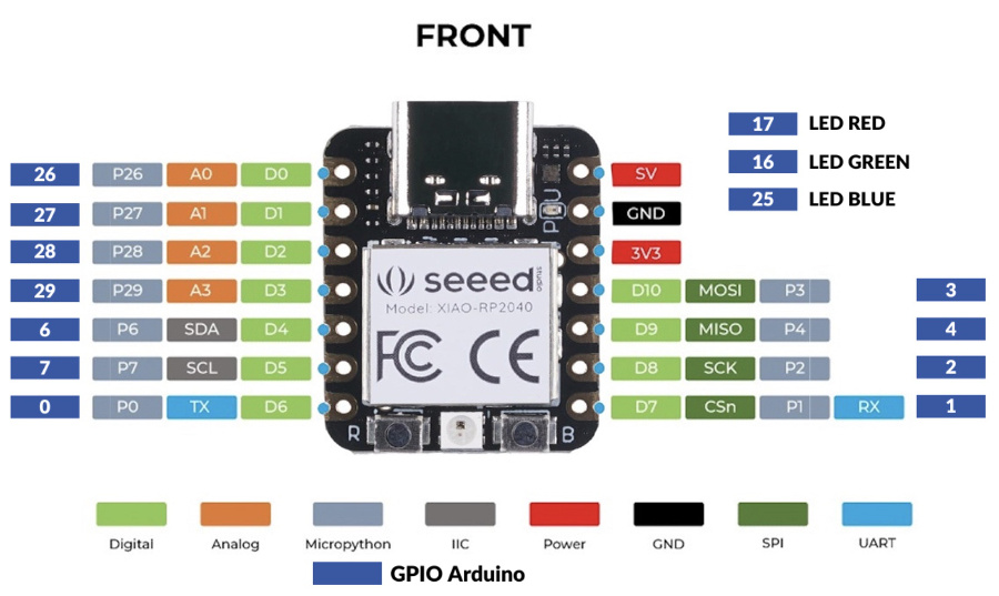
In practical terms and with reference to the schema of the XIAO RP40, following elements will be "expoased":
(*) these 4 I/O PINs can be used in the future to enable SPI communication between boards (communication protocol which will require MISO, MOSI, SCK, CS + 3.3V and GND pins).
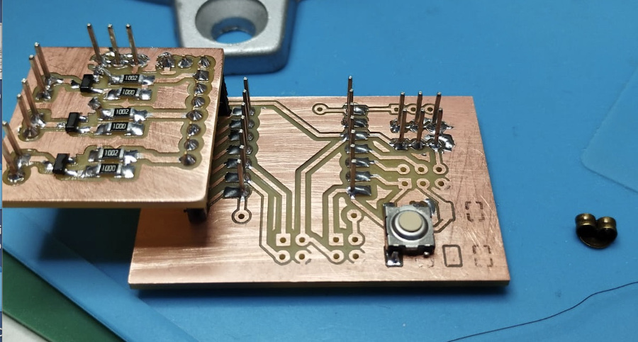
Two button connectors have been connected to the PINs #1 and #2.
To save space, I have not used external pull-up resistors. This has the consequence that if we want to use these buttons, we will activate the internal pull-up resistors via code).
At the bottom, immediately south of the XIAO module, we expose 2 other communication protocols between boards: the I2C protocol (SDA, SCL, 3.3V, GND) and the serial protocol (TX, RX, 3.3V, GND).
In addition to this first PCB, I have created an addition one with the MOSFETs (see image below):
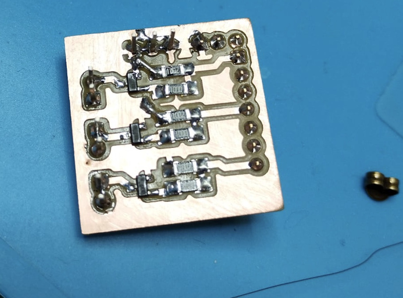
This additional board with the MOSFETs will put us in a position to test any output that requires a large current absorption. There're 3 MOSFETs connected to the PINs #26, #29 and #0. The Drain PIN of each mosfet is connected to 2 pinheads, so you can easily attach anything via jumper cables or via alligator clips. Once the addon board is mounted on the main board we get the pcb + add-on configuration (see photo below):
Set-up to test the Flexinol
The Flexinol is an alloy of nickel an titanium and it cannot be solded with the equipments that we have in our fablab. So the first point to overcome was how to connect this flexinol wire to the board
The first tentative consisted in using earring holders (see image below)
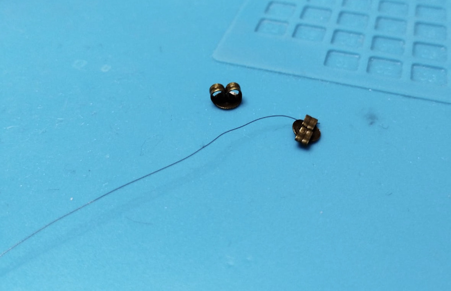 The current continuity is ensured but unfortunately we vannot solder it.
Second tentative was made using tiny copper rivets, used to build homemade dual layer PCBs (see image below)
The current continuity is ensured but unfortunately we vannot solder it.
Second tentative was made using tiny copper rivets, used to build homemade dual layer PCBs (see image below)
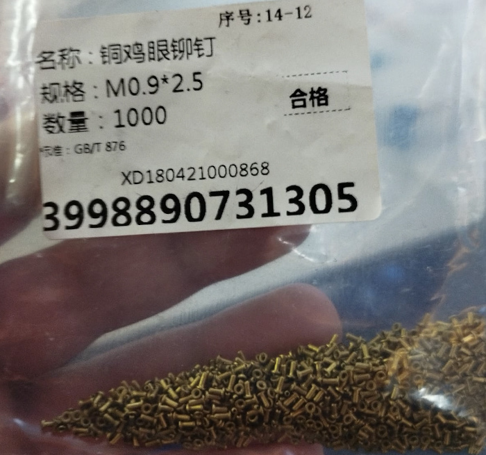
I passed the flexinol thread (diameter 0,37 micrometer) through the rivet hole and crushed them with a hammer (see result of the operation below):
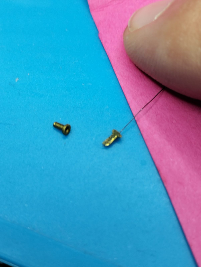
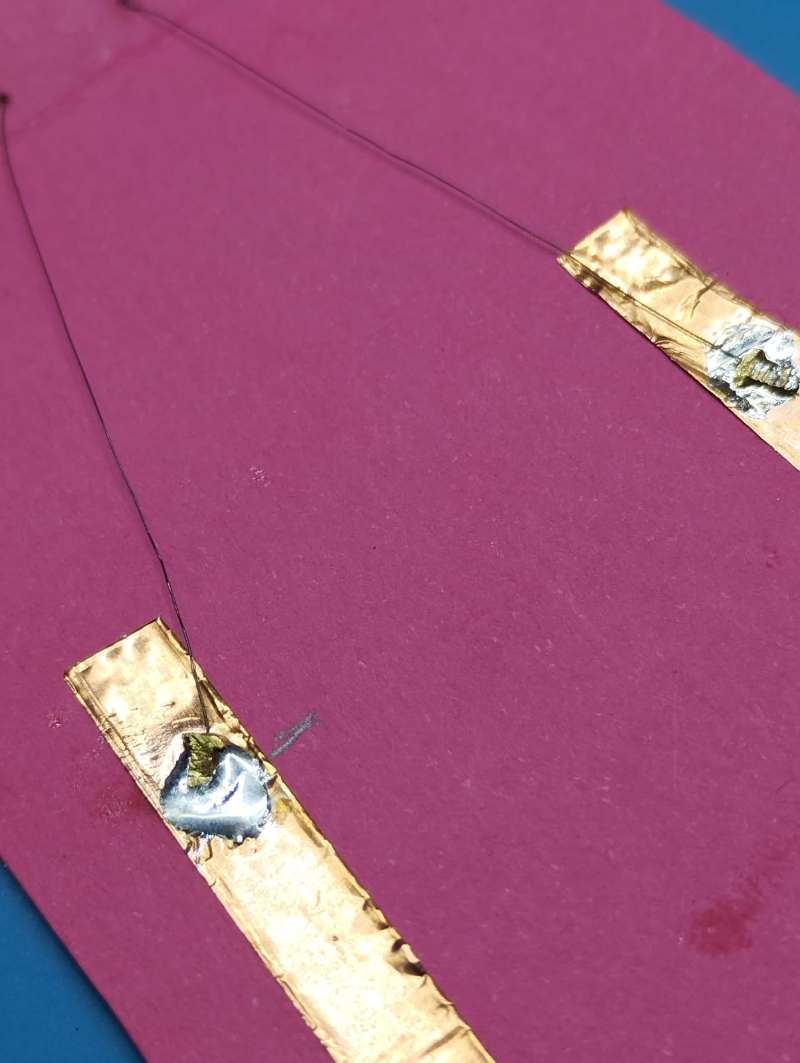
At this point, it was easy to weld everything onto the cardboard (see reults below):
At this point it was easy to connect the set-up with a power source. I have used a LiPo battery (3.7V, 600mAh) that had been previously tested with the multimeter to assess the voltage: 2.9V.
This voltage was close to the theoretical voltage calculated for the test: 3V.
Micropython code created:
Link to the code written in Micropython: link
Link to the python codeThe code is very simple and meant to run the test. The button connector pin has been set as input pin (with internal pull-up), the pin connected to the gate of the lowest mosfet as the output pin, and i used the RGB led mounted on the XIAO to have a visual feedback. When the button is pressed, the LED turns blue and the mosfet is "opened", allowing the battery current to flow through the flexinol, causing its contraction".
Video of the experiment: link