Week08. Electronic production
Good soldering practices:
For people like me who never performed soldering in the past, taking good habits from the very beginning is extremely important
The soldering material:
Soldering station:
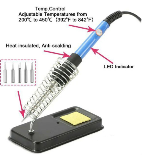
Using a soldering station makes your life easier and is highly recommended.
Types of soldering iron tips:
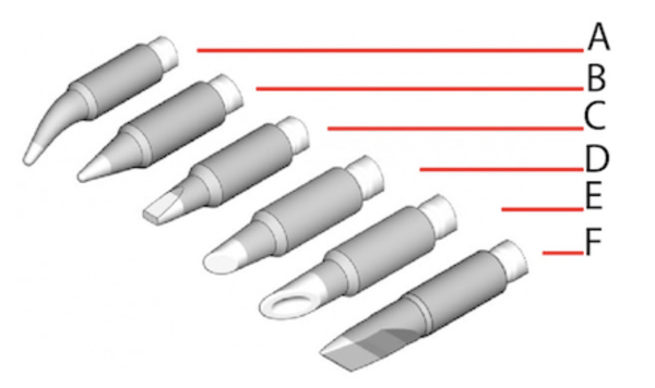
(A) Needle (I-series) tip: the ends of a needle tip are pointed, and hence suitable for applications that involve very high precision => not suitable for soldering large components.
(B) Conical (B-series)tip: a conical tip has a conical taper with a rounded end and delivers heat to a small defined area. The tip can be used for flexible applications and the soldering can be performed from any angle. Conical tips are used for general purpose applications.
(C) Beveled tip: a beveled tip is similar to a conical tip with two of its ends flattened to resemble a ground-up pencil. The flat sides can hold more solder as compared to a conical tip and can be used to transfer a lot of heat to more demanding joints. A beveled tip is highly versatile, hence useful for everyday use.
(D) Chisel(D-series): a chisel tip is similar to a beveled tip, but only one side is flattened. The tip resembles a chisel and has a larger surface area compared to a conical tip. These tips are used in applications that require a lot of heat transfer, like soldering thick wires, or even desoldering.
(E) Hollow Point tip: similar in looks to the chisel type tips, these tips allow for correcting bridging. The tips have a spherical indentation where the chisel type is flat.
(F) Knife (K-series): a knifetip has a slanted tip, thus resembling the shape of a knife. These tips are typically used for drag soldering, where the tip is dragged across many pins on an integrated circuit, to increase the soldering accuracy and efficiency. A knife tip is also suitable to fix solder bridges.
Do not forget to add water on the sponge of the station before starting your soldering work. After you are certain that the tip is totally coated in solder, wipe the tip off on the wet sponge to remove all the flux residue. Do this immediately so there is no time for the flux to dry out and solidify.
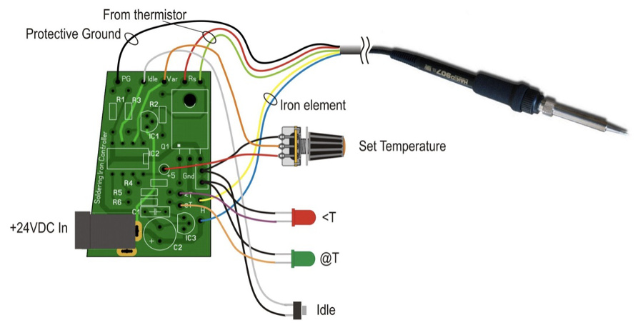
Just to reconnect to the week we learned about electronic design, below a simplified project of the soldering iron and station with heat regulation, temperature sensor (thermistor):
Soldering lead types:

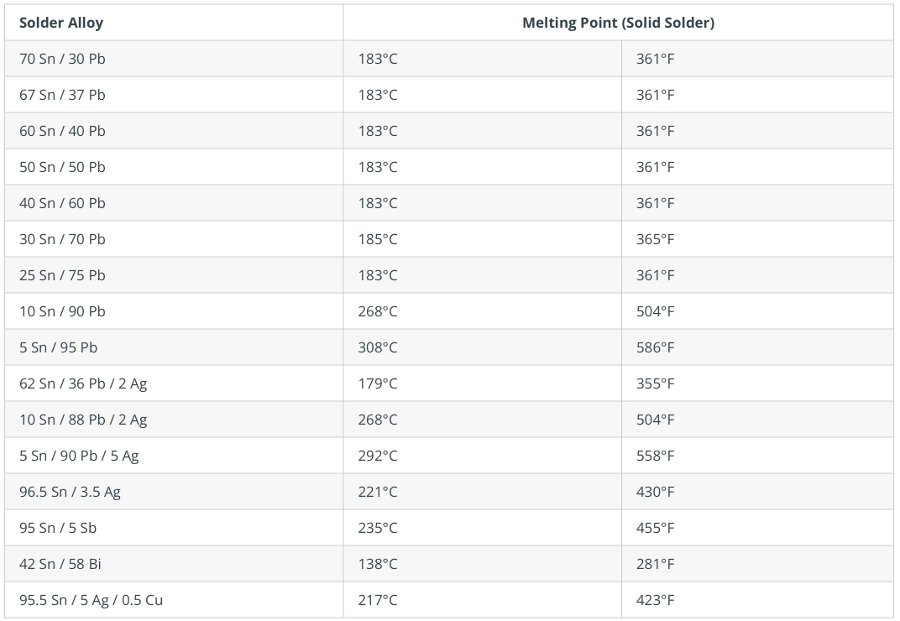
The filler element is nothing but the Solder, which is a metal alloy. Solder Alloys usually consists of the following elements: Lead (Pb), Tin (Sn), Silver (Ag), Bismuth (Bi), Antimony (Sb), Indium (In), and Cadmium (Cd). Lead (Pb) and Tin (Sn) are the main elements generaly used for soldering electronic components. Lead (Pb) usage is decreasing rapidely due to its toxicity but is still largely used for small projects.
The key criteria for selecting a Solder is that the melting point of the solder should be lower than the melting points of the metals that have to be joined/p>
The melting point of the solder depends on the mixture of alloys. Below a summary of the melting points for the different types of alloys:
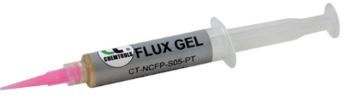
Soldering flux:
The soldering flux has to be used systematicaly in soldering or desoldering processes. This flux removes an oxide film on the surface and as a consequence it It increases the wetting ability of the solder, causing it to flow more uniformly over surfaces without balling-up (dewetting).
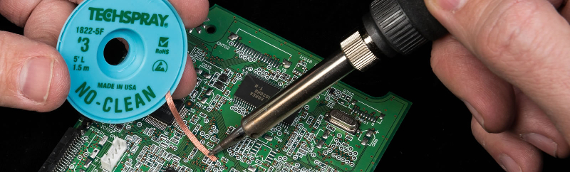
Desoldering wire braid solder remover:
How to use it: simply place the end of the wick over the solder you want to remove and then place your heated solder tip over it. The braid heats up and encourages the solder to “wick” into it.
>
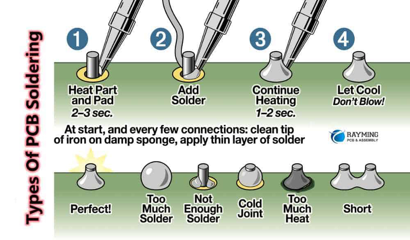
Very good summary and visual representation found on the web illustraying good and bad soldering:
 ///ADDD different key steps of the soldering process: https://www.instructables.com/Simple-PCB-soldering/
Key steps to follow in the soldering process:
1. Place the component in the hole on the board as per the marking, and fix it in the position by bending the leads.
2. Switch on the power supply of the soldering iron and wait for the tip to get heated. This might take a few minutes.
3. Place the solder on the board and touch the tip of the iron on the solder for a second so that it melts.
4. Remove the iron and solder wire.
5. Check whether the joint formed by the solder is proper. A good solder joint will be conical in shape. If the shape is not formed correctly, cut off the component lead and perform the process once again.
6. If the solder forms sticky chunks instead of getting melted properly, it might be due to oxidation at the soldering iron tips. Tinning the iron is highly recommended, at least before and after the soldering process
Source: https://tameson.com/pages/soldering-iron-tips
Key quality atributes for good solder joint quality:
Always keep in mind that safety comes first when soldering !!!

PCB production:
The most standard way to produce PCB is etching: it consists in removing copper from the surface of the PCB to reveal the desired circuit pattern. During the ectching process, all copper is removed except for the circuitry that is protected by tin plating.
PROs of etching: batch process, very high resolution. CONs:etching is not a sustainable process, it implies a huge water consumption and production of nasty chemical wastes. The set-up for etching is pretty heavy
Mainly for the heaviness of the set-up process, we will be using the machining and a table-top milling machine that will mecanicaly remove the material.
Using milling machine is not the fastest process but the simplest in terms of set-up. In addition, the waste is not creating risks from a hazard perspective.
We will be typically producing PCBs with only one layer and to overcome wire cross-overs, we will use 0 ohm resistance as a workaround.
The milling machine is offering advantages compared to the breaboards: the breadboards have poor electrical performances. Any move of a breadboard set-up usually leads to a malfunction of the system and requires troubleshooting
Accuracy of the milling machines is reasonably high: in the range of 0.010 inch
Assignments
Group assignment:
characterize the design rules for your in-house PCB production process extra credit: send a PCB out to a board house
Individual assignment:
make and test the development board that you designed to interact and communicate with an embedded microcontroller. extra credit: make it with another process
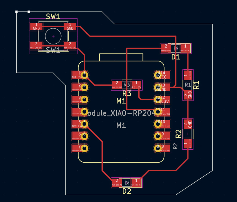
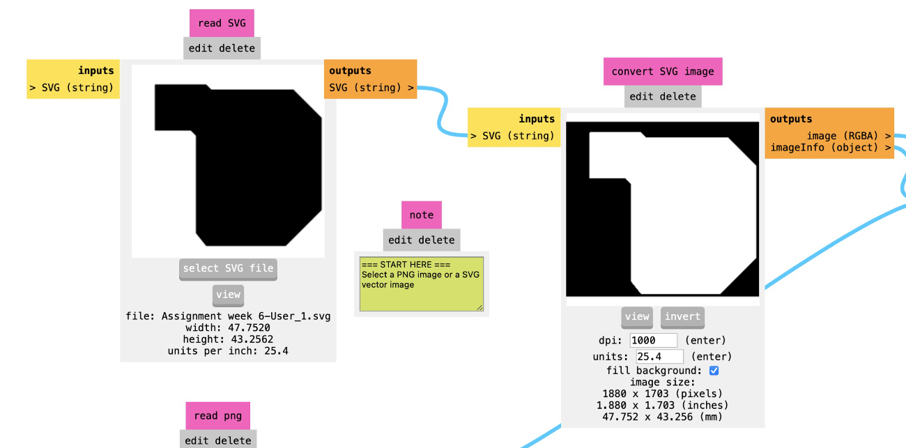
Let's take the .pcb file of the PCB we had designed during the week06- Electronic Design.
Run KiCAD
Open the pcb file
For a sake of verification, I first re-ran a DRC check on the .pcb file and no error came-out. So green light to proceed with next steps
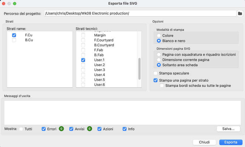
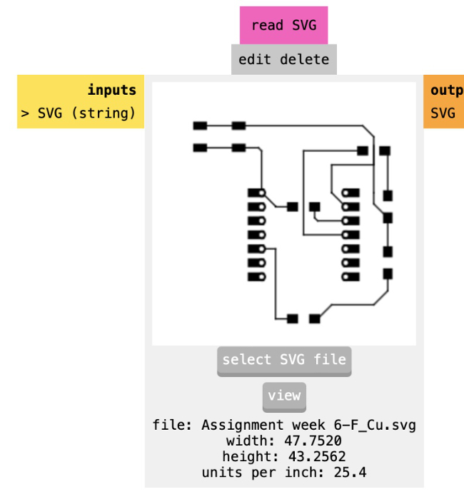
Then the next step is to export the KiCad project into .svg file(s)
Selection of the F.Cu layer
File => export => SVG
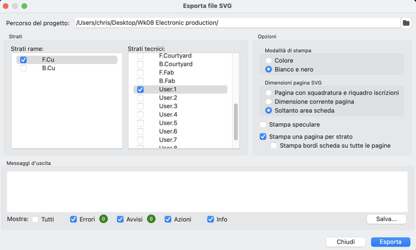
Selection of the User.1 layer
File => export => SVG
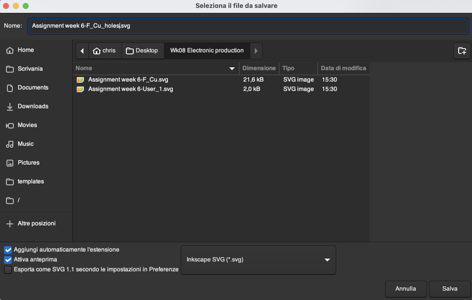
Two files have been created in my local directory:
Next step: download and installation of INKSCAPE tool
INKSCAPE is Inkscape is an open-source vector graphics editor that we will be using to re-treat the .SVG files

/////
Next step: transformation of .SVG files into specifc .GCode format used by the Roland milling machine (Roland SRM-20) that is available in our FabLab in Siena
For this purpose, FabAcademy has luckily developed an online platform called modsproject (https://modsproject.org)
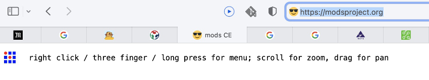
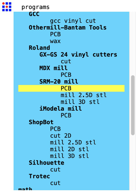
Follow the path: Programs > Open program > Machines > Roland > SRM – 20 > PCB

Overview of the workflow:
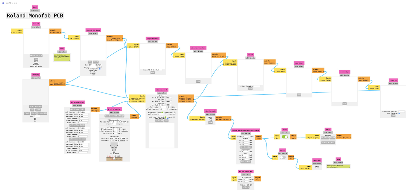
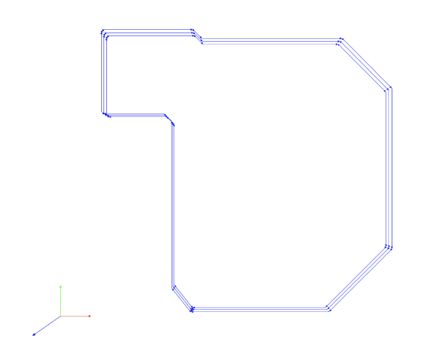
Open the .SVG file corresponding to the traces:

In the section "Origin" of the workflow, modify the values of the x,y,z initially valued 10 to zero.
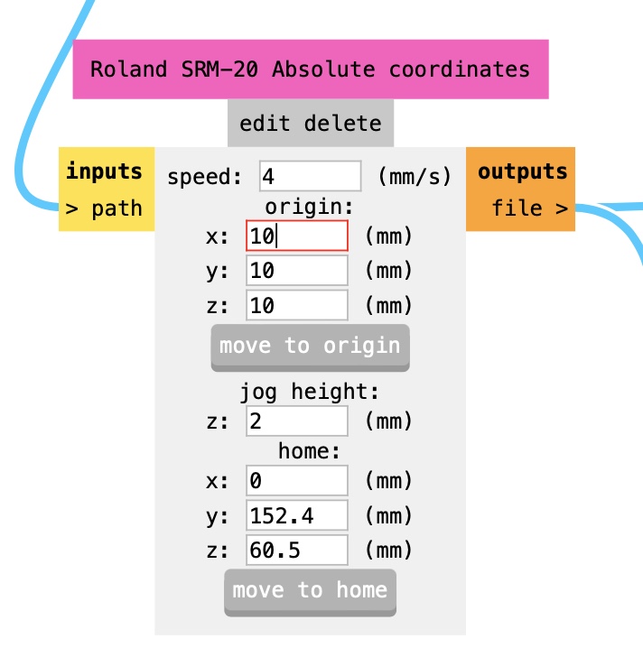
The jog height parameters must be kept and should never me modified.
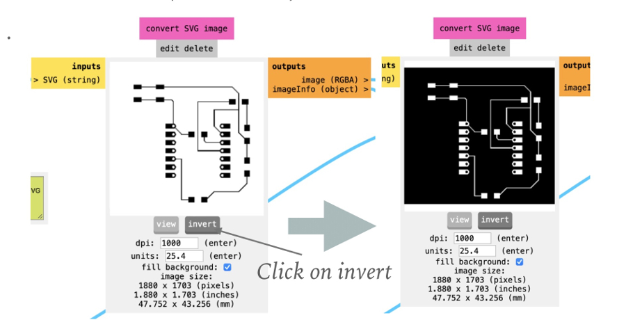
Important note: on the diagram, by convention the milling machine will remove the material on all the "black" parts
So do not forget to click on "Invert" in the "Convert SVG Image" menu to have the correct set-up
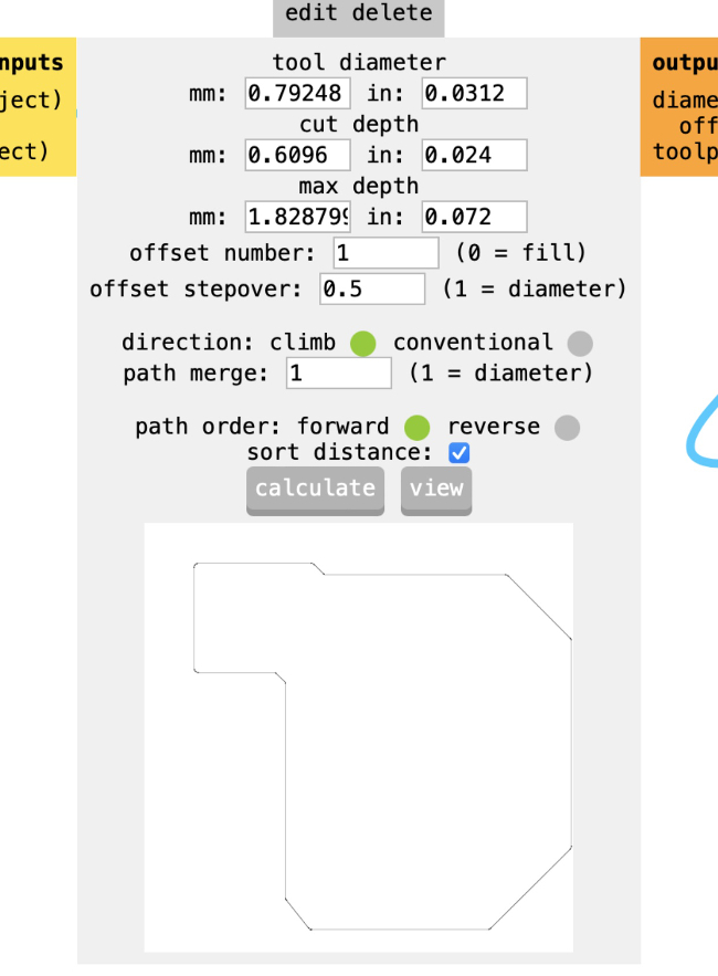
Set-up the correct values in the menu "Set PCB Default"
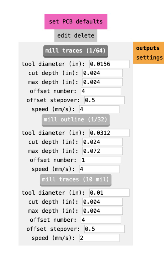
When you have done with the modification / check of the parameters, click on "calculate" to generate the .GCode file.
"Max depth" is always a multiple of "cut depth"
"Offset number": 4 (by value)"
"Offset stepover: 0,5 (by default). Stepover parameter has a key stake in the quality.
The difficulty is to find the right balance between speed (4 mm/s for instance, depth cut and offset stepover:
When it comes to the machining time, consider that the total length of a toolpath will approximately double if you cut the stepover in half
That's why it makes sense to run different experiments to understand if cutting the stepover in half double the quality of my part
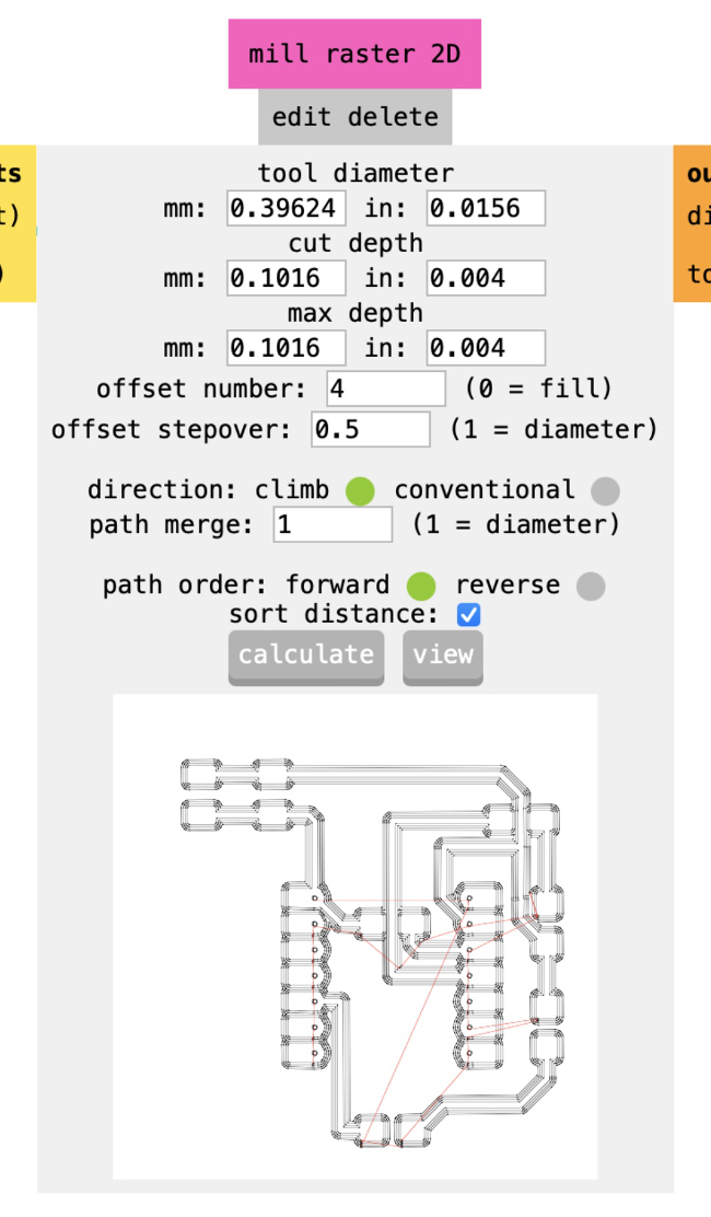
Click on View to visualize and check the overall path of the milling bits
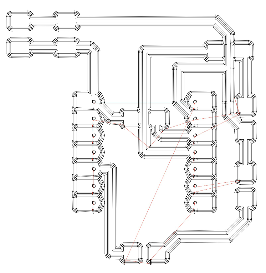
After completing final checks, I saved the files on my local folder and transfered them on a USB key
Export on USB key of .rml trace file readable by Rolland machineSimilar steps have to be repeated for the outline .svg file of the outline layer of the PCB project
Open the .SVG file corresponding to the outline:

Similar steps were executed for the holes file generated with Inkscape.
Due to the fact that in the end, the holes were created with the milling column (see photo below), I did not inserted the screenshots of the activities in Mods related to the creation of the .rml files for the holes layer
PCB milling using the Roland SRM-20
The main PCB boards that we use to mill our PCBs are FR1 board (dimensions to be added) and FR2 (140mmx90mm) that are low-costs PCBs that have the great benefit to be contituted of materials that are not hazardous (always remember that safety comes first !). The milling process will remove part of the copper layer of the FR1 board according to the scheme created with KiCad in order to create the electric wires and pathways
We use to dimensions of mill bits for our assignment:
Milling machine set-up:
Do the proper set-up of the Roland SRM-20 using the VPanel Desktop.
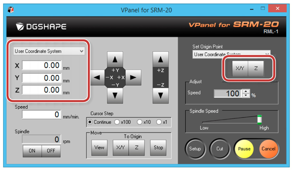
Before executing any milling operatioon, do not forget to set the origin point. It means that you have to set the origins for the 3 dimensions: X, Y and Z.
The X and Y origins are determined by the cutting data and the location of the PCB board while you normally align the origin Z with the surface of the material.
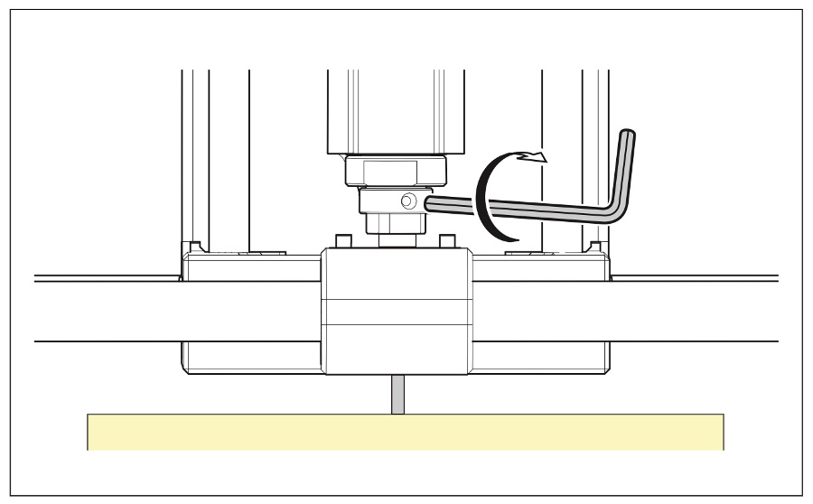
Loose the set screw, and then adjust the cutting tool so that its tip contacts the surface of the material (see image below):
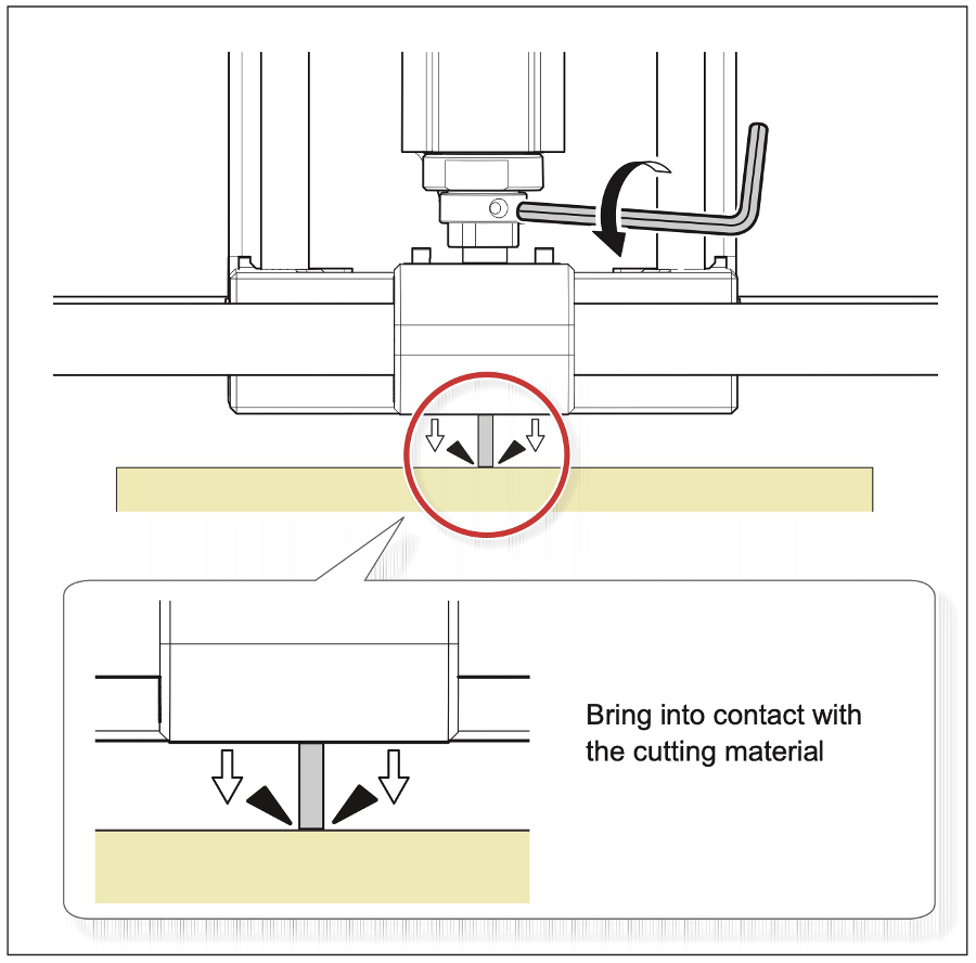
Tighten the cutting tool in place again with the set screw.
Always keep in mind to take the size of the material and the length of the cutting tool into consideration when you setting the origins !! in this way you will avoid damaging the milling tips .
Important to note that you need to keep X/Y origins the same during the overall process (wire, holes, outline) while Z origin whill be changed at each process step and change of the milling bit
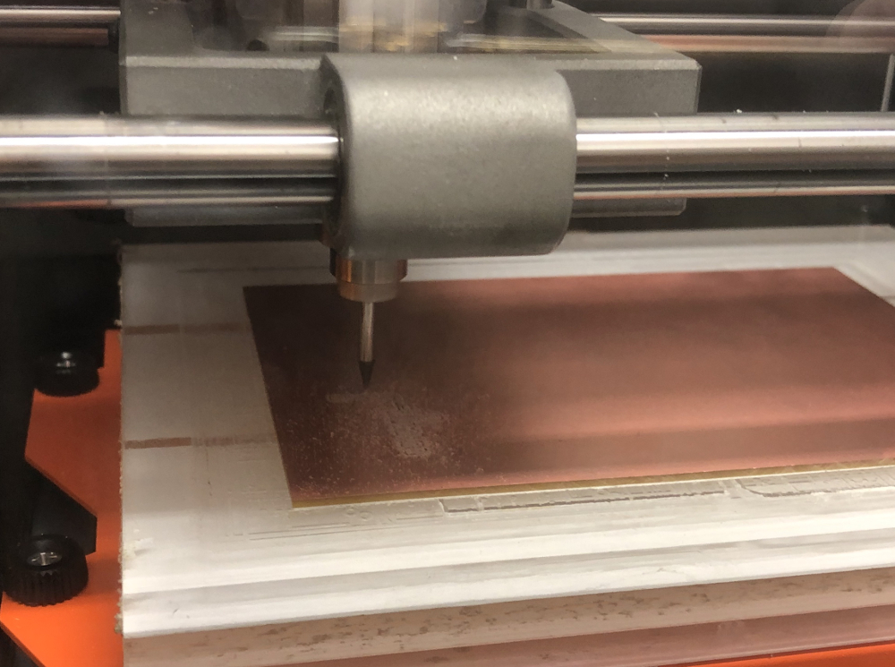
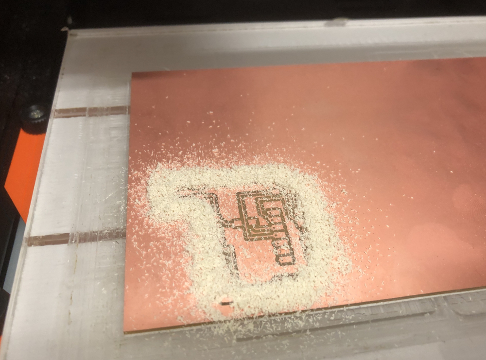
Milling operations sequence:

The first attempt using a FR1 board was not successull. Despite the use of double-sided tape, the plate gradually detached and began to vibrate. Since the milling operations did not proceed correctly, I decided to kill the process.
For the second attempt, I have used a wider plate leading to avoid that it would detach from the surface.
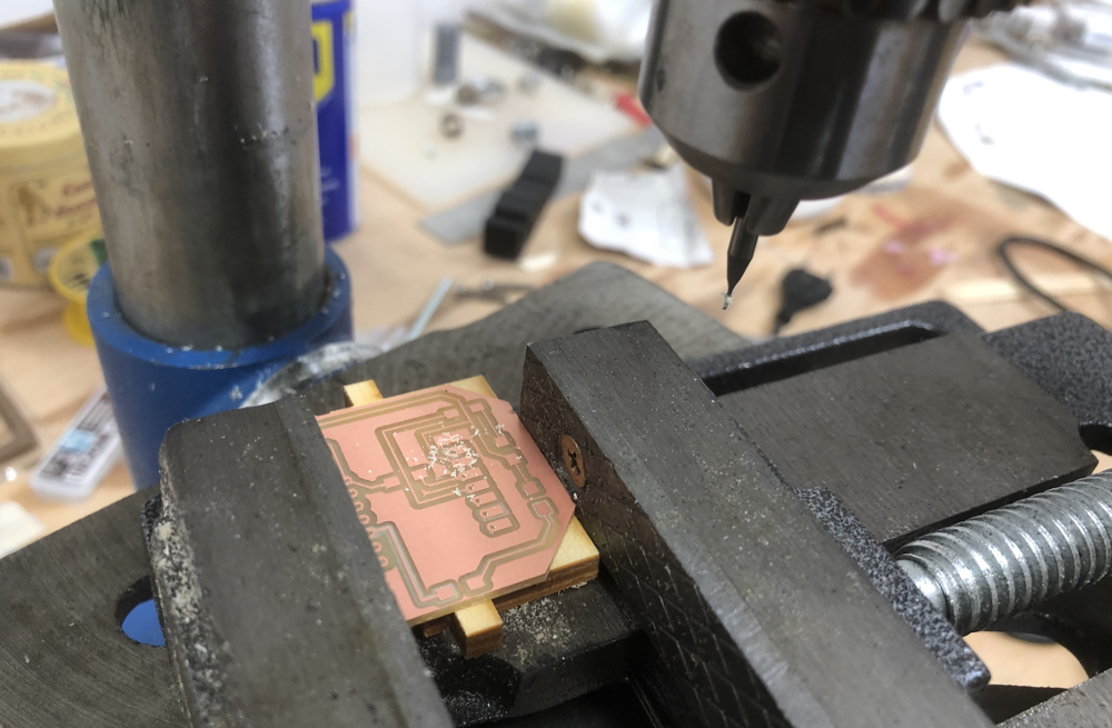
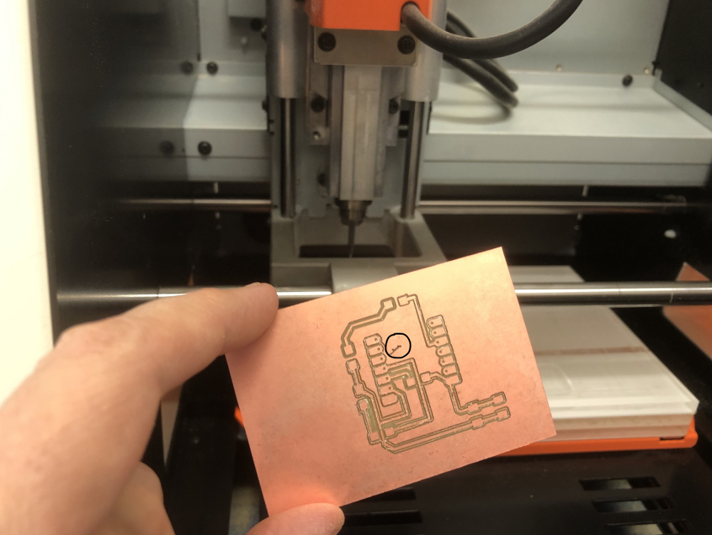
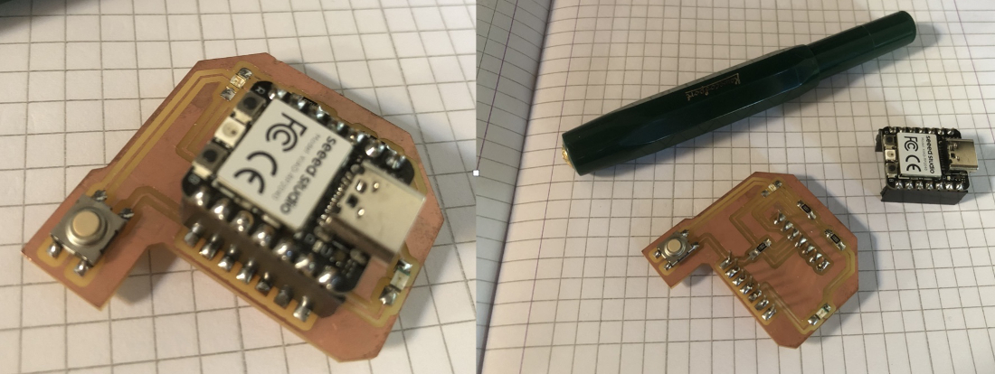
The PCB just milled is definitely ok after accurate visual check.
In the end, we have decided to go manual for the creation of the holes and it was successfull at the first attempt :)
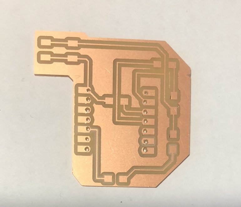
The PCB has been finally cleaned with tepid water and dried with a tissue paper.
Soldering the components.
As previously mentioned, it was the first time that I had the opportunity to perform soldering activties.
Activities proceeded smoothly without issue to be mentioned. It took about 1,5 hour to get soldering activities done.
At completion of the soldering activities, I have cleaned the PCB with alcool since FLUX would corrode the PCB.
Basic checks were performed on the PCB: visual inspection and some continuity checks with the voltmeter.
Programming the newly created PCB:
The PCB inludes 2 LEDs (one RED and One Blue) and one connector.
One Led Blue / red on PIN #5, one LED Blue / Red on PIN #11, one connector on PIN #1
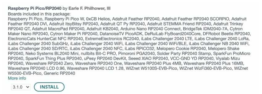
Installion of Seeeduino XIAO board to Arduino IDE
Run Arduino IDE & Navigate to File > Preferences, and fill “Additional Boards Manager URLs” with the url below:
https://github.com/earlephilhower/arduino-pico/releases/download/global/package_rp2040_index.json
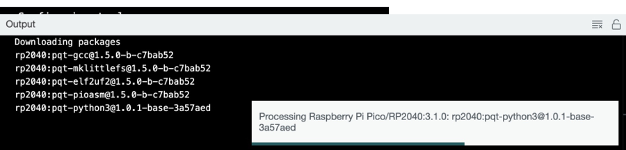
Download and installation of the packages successfully completed
Programming the PCB
To test our PCB with the connector and the 2 LEDs, a simple firts peace of code has been created using Arduino IDE:
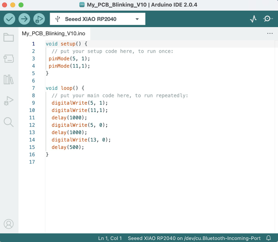
Verification of the code written using the proper button on the menu Bar.
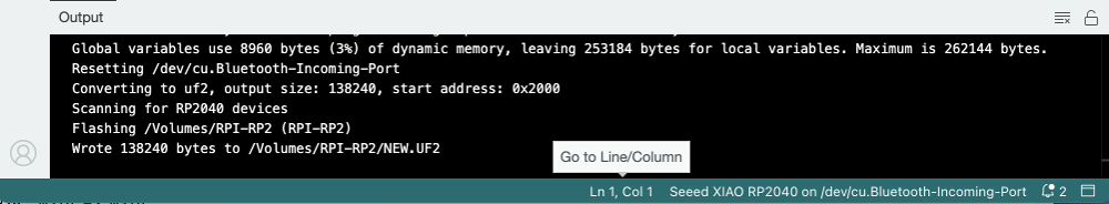
Since verification is successfull, we can use the upload button to push the Arduino code to the XIAO rp2040 connected through the USB port/p>

As per screen below, the upload on the rp2040 was successfull:
 // tutorial: https://docs.arduino.cc/library-examples/curie-ble/Genuino101CurieBLEButtonLED