6. Electronic design
key learnings.
Electric laws.
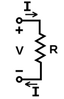
Ohm's law:
States that the current (I) through a conductor between two points is directly proportional to the voltage (V) across the two points. The law Introducins the constant of proportionality, the resistance (R): I = V x R
 Source Wikipedia
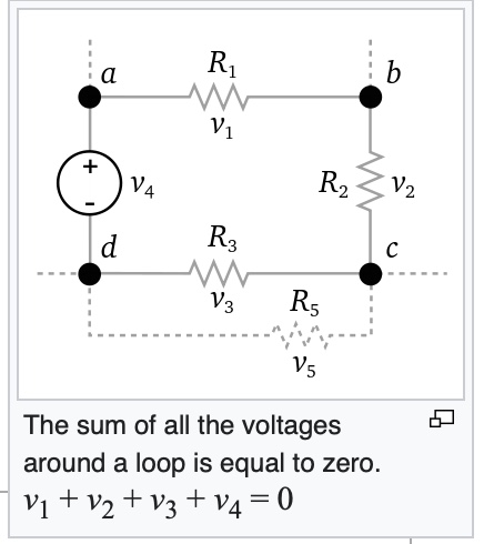
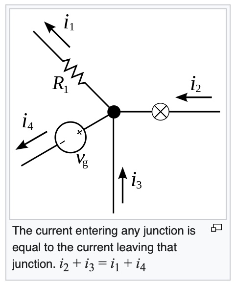
Kirchoff's laws
 Source Wikipedia
Week 06 group assignemnt:
Use the test equipment in your lab to observe the operation of a microcontroller circuit board.
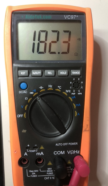
We started our session in the lab with a quick review of the Voltmeter main functionalities
Snapshot of the Voltmeter available in Santa Chiara Lab:
Voltmeters use cases in a nutshell:
For the measurement of the voltage between two points:

Measurement of the voltage between two points:

To test the electric continuity:

To test the capacitance of a capacitor:

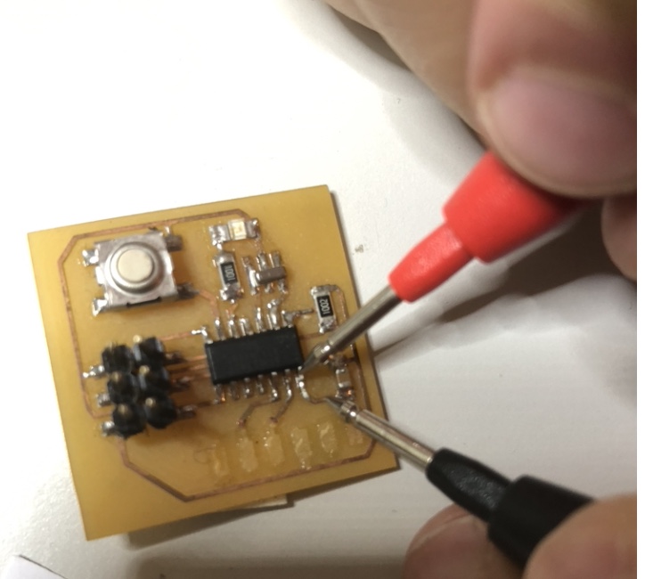
We performed a test of continuity. We took a PCB built in the lab and controlled that there was continuity between one PIN of the micro-controller and the wire:
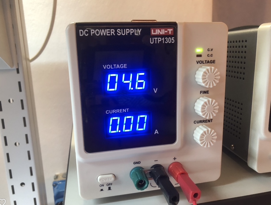
Then we went through the functionalities of the Bench Power Supply (model UTP 1305)
This power supply equipment can manage current in the range [0,32V] and voltage in the range [0,3A]
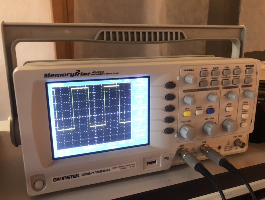
Then we did received explanations on the oscilloscope equipment.
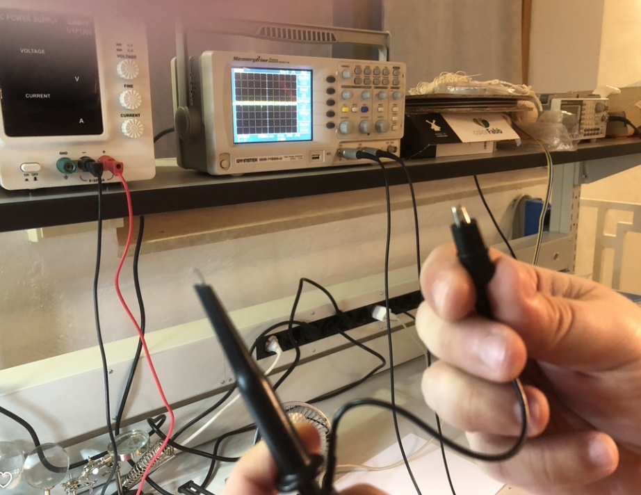
An oscilloscope (informally a scope) is a test instrument that graphically displays varying electrical voltages as a two-dimensional plot of one or more signals as a function of time. The displayed waveform can then be analyzed for properties such as amplitude, frequency, time interval and others....
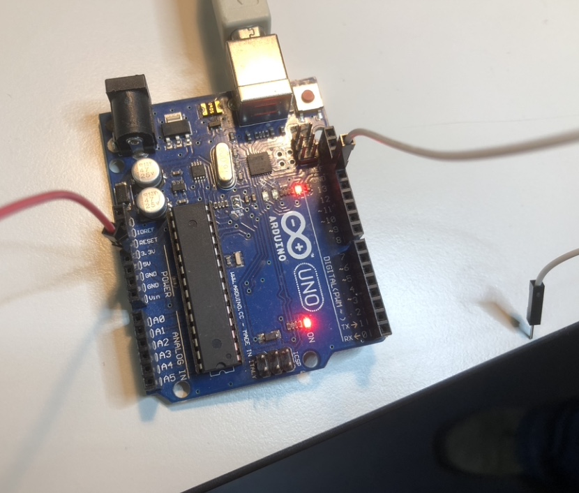
We did some hands-on with the oscilloscope. We took an "Arduino UNO" that had been programmed to make a Led blink every 500ms
We calibrated the oscilloscope correctly to be able to display the max voltage (5V)getting confirmation that every 500ms, we had 5V signal and 0V for the coming 500ms
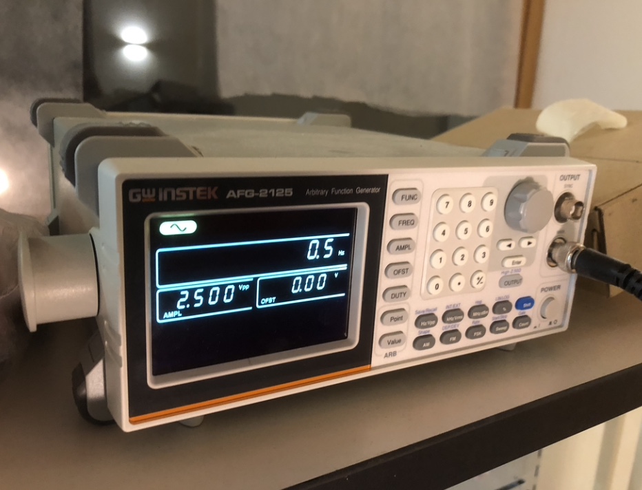
At the end of the session we received information related to the function generator that we will be using in our activities
Individual assignment:
The assignment consists in the design a development of a PCB to interact and communicate with an embedded microcontroller.
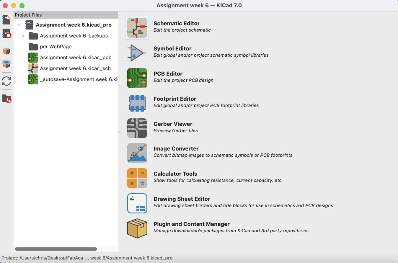
To complete the individual assignment for this week I have used KiCad SW
KidCad EDA
KidCad is a freely available, Opensource and cross-platform tool. KidCad is a suite of different SW that are integrated
KidCad main page
I had to upgrade my MAC OS to a newest version (12.6) to be able to import the Fabacademy libraries of components. It took around 5 hours to complete downlad and installation of this 12.4 Gb SW package
Right after MAC OS updrade and before starting a new project, the following two key libraries have been imported into KiCad:

Step 1: logical design using KidCad schematic editor.
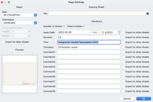
First of all, I have created a new project "Assignment week6 Fabacademy 2023.sch" and updated the project properties:
Then the components of the project were added using the "Add Component symbol" button:

Below the list of components integrated on the PCB:
After adding the components, the wires between the components have been created using the button:

Important note: I did not face overlaping of the wires for this project. In case such trouble would occur, use the Tagging option accessible with this button:

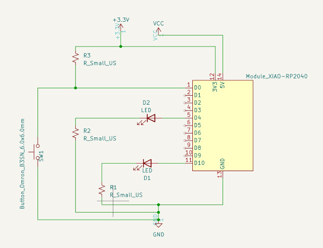
Overview of the final schematic when completed:
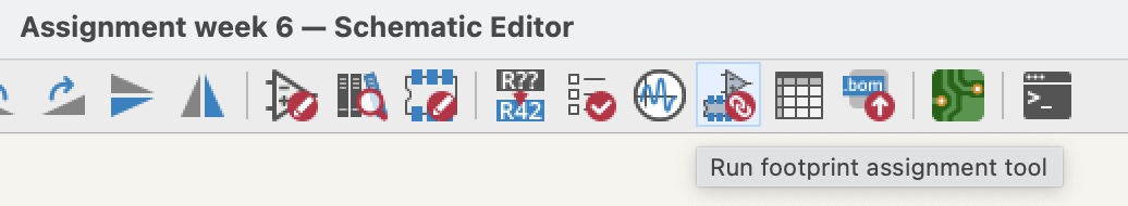
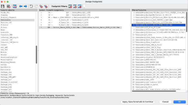
Step2: assignment of the footprints to the components
Following button has to be pressed to start the footprint assignment process:
Then when the footprint assignment process is done, it's time to update the PCB from the schematics.
View available after update of the PCB:

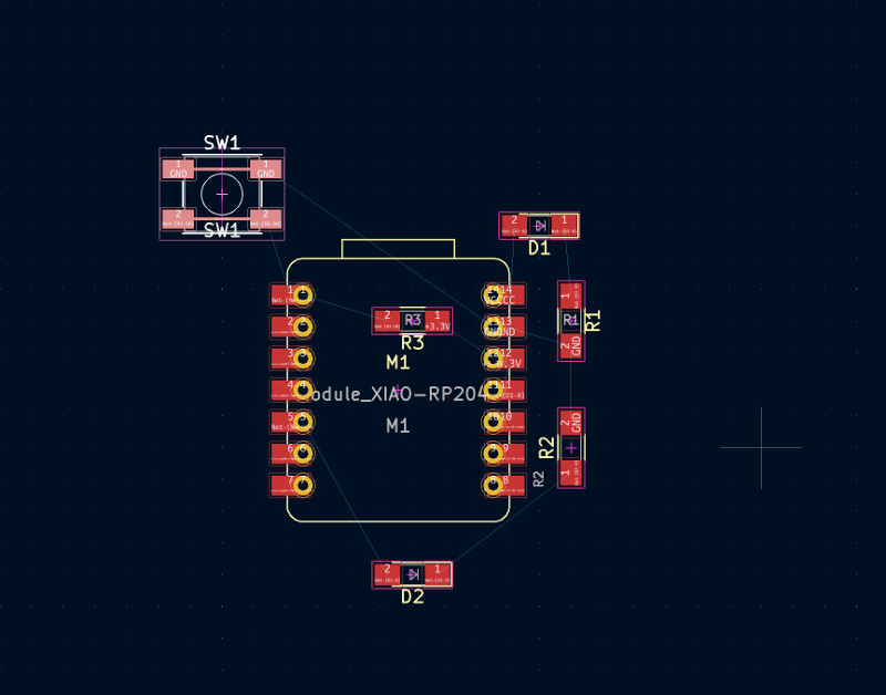
At completion of the process, following preview is available:
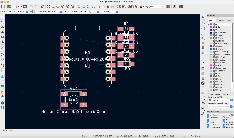
At this point, I started the manual move of the components to remove all tracks crosses:
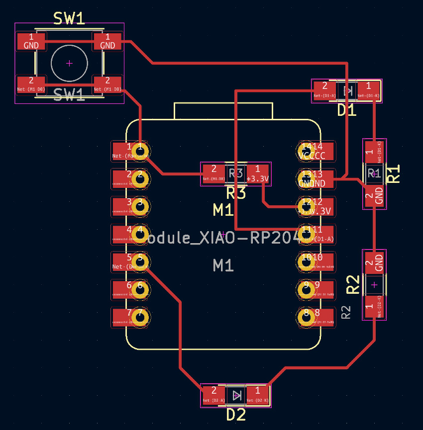
At this point, I proceeded with the operations of routing using the "route tracks" button

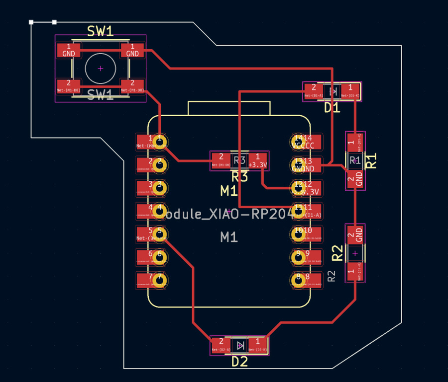
Then I defined the edges of the PCB using the dedicated button
Final result of the PCB with the edges cut:
At this stage, I ran a DRC check and no errors came out:
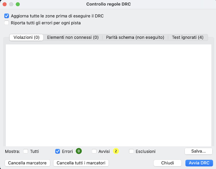 Week06_DRC_Check_OK
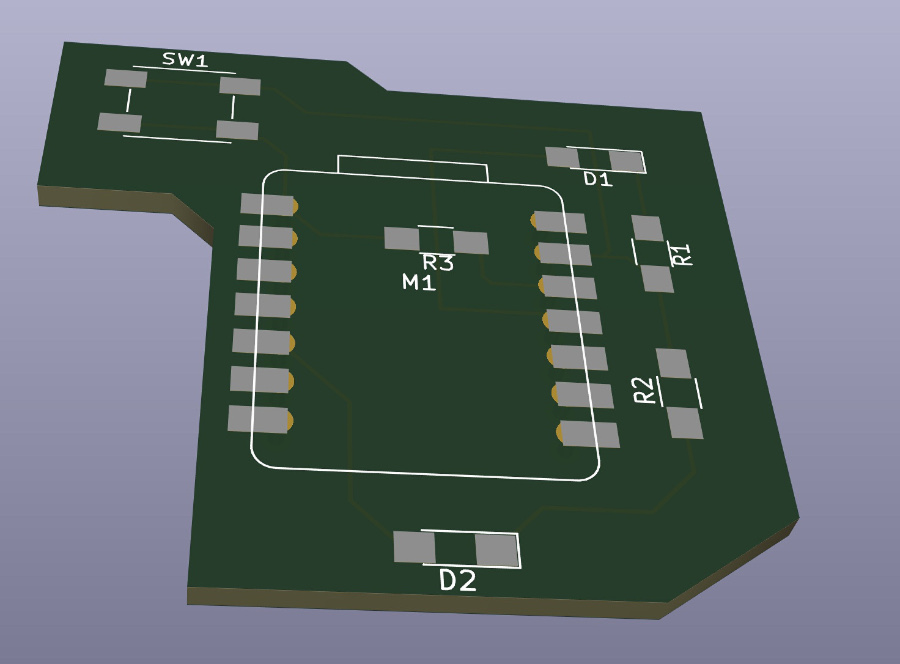
3D preview of the newly createed PCB:
KiCad files related to this assignment:
Files rml for the milling activities on the Rolland machine: