Electronics Production
Assignment to be done:
1.Group Assignment:
Characterize the design rules for your in-house PCB production process
extra credit: send a PCB out to a board house
To be found here
2.Individual Assignment:
Make and test the development board that you designed
to interact and communicate with an embedded microcontroller
extra credit: make it with another process
1. Reflection on what I learned from Group Assignment
The design rules for PCB production process
There are a number of design rules that should be followed for in-house PCB production process:
Trace width and spacing:The width of the traces on the PCB and the spacing between them will depend on the current and voltage levels that they will be carrying. These parameters are typically specified by the design engineer and will be used to determine the minimum trace width and spacing.
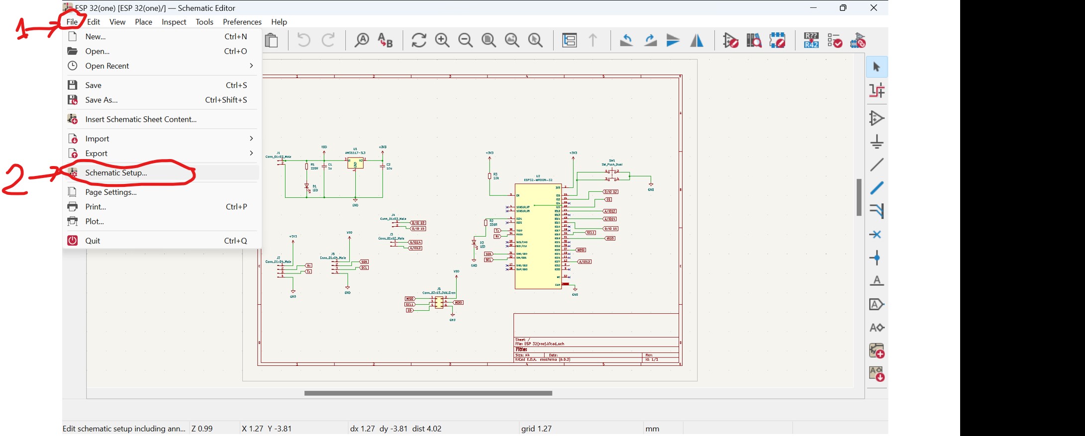
By clicking on schematic setup, its windows opened and choose Net classes and it opens with the name of defaul is named by default then start changing different parameters as you wish. Refer to the image below:
Plunge rate:The plunge rate refers to the speed at which the bit plunges into the material. You'll want to use a slow plunge rate to avoid damaging the bit or the material.
Depth of cut:The depth of cut is the amount of material that the bit removes with each pass. You'll want to use a shallow depth of cut for fine details and a deeper depth of cut for larger cuts.
Traces:The width of your traces will depend on the size of the bit you're using and the spacing between the traces. Generally, you'll want to use a smaller bit for finer details and a larger bit for larger traces.
Outline:The depth of cut for your PCB outline will depend on the thickness of your PCB material. You'll want to use a shallow depth of cut to avoid cutting through the material completely.
Tooling:You'll want to use high-quality milling bits that are designed specifically for PCB milling. These bits should be sharp and precise, and they should be able to withstand the rigors of milling PCBs. You may also want to consider using a dust collection system to reduce the amount of dust and debris generated during the milling process.
Hole size and placement: The size and placement of holes in the PCB are important design parameters that must be carefully considered. The size of the hole will depend on the component that will be mounted in it, and the placement of the holes must allow for efficient routing of the traces.
Via placement and size:Vias are used to connect the different layers of the PCB together. The placement and size of the vias must be carefully considered to ensure that they do not interfere with other components or traces on the board.
Pad size and shape:Pads are used to connect components to the PCB. The size and shape of the pads must be carefully chosen to match the component that will be mounted on them.
Silkscreen and soldermask: Silkscreen and soldermask are used to label the components on the PCB and protect the traces from solder bridges. The design of the silkscreen and soldermask must be carefully considered to ensure that they do not interfere with the placement of components or the routing of traces.
Design for manufacturability:The PCB design must be optimized for manufacturability. This means that the design must be easy to manufacture, test, and assemble. The design should also be optimized for the specific manufacturing process that will be used, whether it is traditional PCB fabrication or a newer technology like 3D printing.
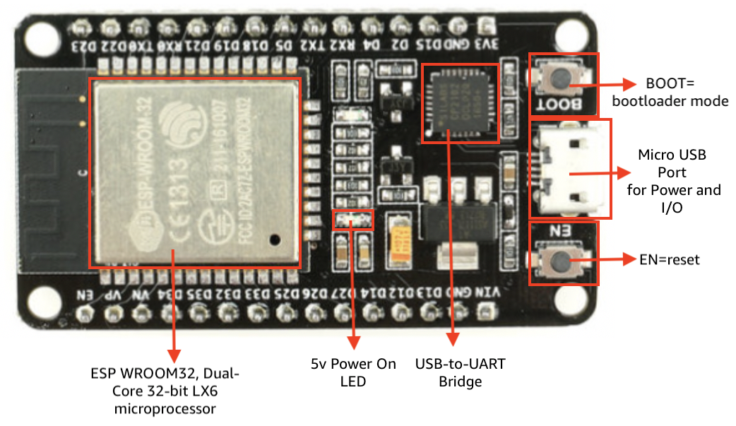
What is development board?
A development board is essentially a printed circuit board with circuitry and hardware for experimenting with specific microcontrollers, microprocessors, or other complex integrated circuits (IC).
A development board is a circuit board that is designed to help developers prototype, test and develop new hardware or software projects. Development boards typically come with a range of features and components such as microprocessors, memory, input/output interfaces, sensors, and communication interfaces that allow developers to experiment with and test various configurations and functionalities. Development boards can be used for a wide range of applications, from designing and testing embedded systems for Internet of Things (IoT) applications to developing new firmware and software for microcontrollers and other electronic devices. They are typically designed to be easy to use and configure, with support for common programming languages and development tools, making them an ideal tool for hobbyists, students, and professionals alike.
Specifically, an IoT development board includes:
A programming interface to program the microcontroller from a computer. A power circuit used to provide stable DC power to the microcontroller. Input components: buttons, switches, etc. Output components such as LEDs. Various I/O pins used for compatibility with sensors, motors, screens, and any other components.
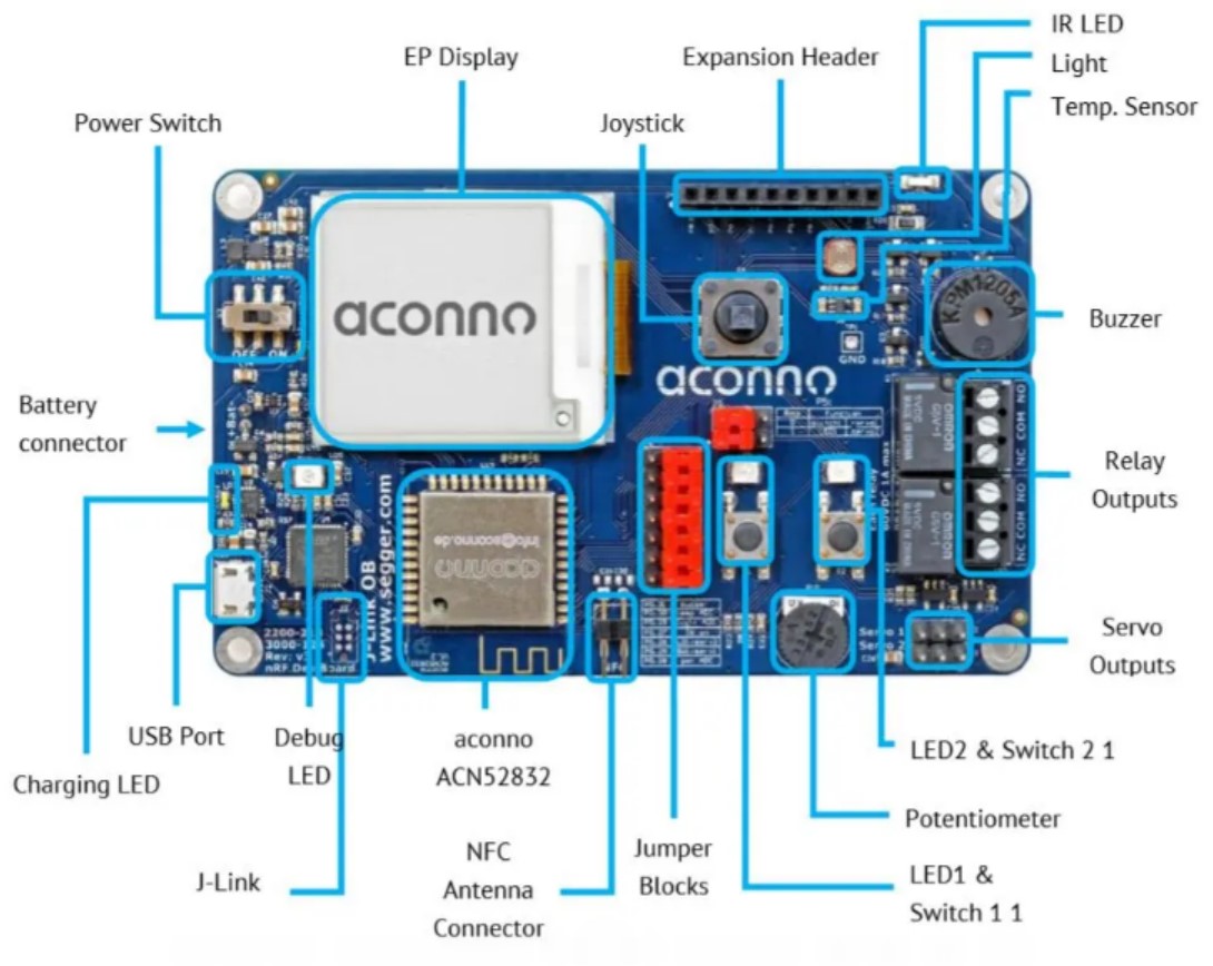
Image below is a typical example of microcontroller board that shows the main parts
There are three devkit categories:
1.Microcontroller - based boards comprised of a small computer, usually built with CMOS processes. These are primarily used in implants, office machines, power tools, and automotive control systems.
2.System-on-Chip SoC boards have more system components integrated into the chip and have memory, audio receivers, PCI, SATA, and USB communication abilities in addition to a microprocessor. Additional electronic components and circuits are the only things required–fewer additional ICs. They allow for more miniaturization and higher processing speeds with less microchip power. This is all at the cost of specialization and development time.
3.Single Board Computers (SBCs) contain all the features of a computer on a single device, including I/O ports, microprocessors, and memory. SBCs are usually larger but are more capable and do not need to rely on expansion slots for additional peripheral capabilities. By refering from Here
Steps to develop a development board
Developing a development board requires a comprehensive understanding of the target microcontroller, programming languages, hardware design, and circuitry. Below are some steps to develop a development board:
- 1. The first step is to identify the microcontroller that you want to use on the development board. Select a microcontroller that is suitable for your project requirements.
- 2. After identifying the microcontroller, create a schematic design for the development board.
ESP32 Board Guide
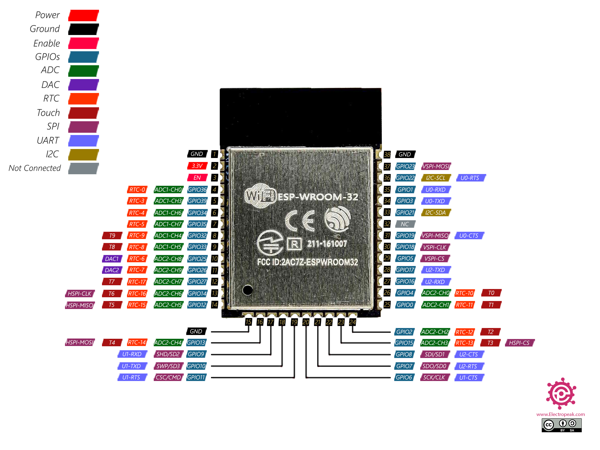
The ESP32 supports three types of I/O modes with each GPIO Pin: Digital, Analog and Internal Sensors
Analog: Used to send/receive analog data using the following functions:
# examples based on Arduino IDE
analogRead();
analogWrite();
Digital: Used to send/receive digital data using the following functions:
# examples based on Arduino IDE
digitalRead();
digitalWrite();
Internal Sensors: This mode allows us to fetch internal sensor data from the ESP32 itself. The three sensors available are as follows:
Internal Temperature Sensor
Hall Effect Sensor
Touch Sensor
These sensors can be accessed by the following functions:
# examples based on Arduino IDE
temprature_sens_read()
hallRead()
touchRead()
reference from here
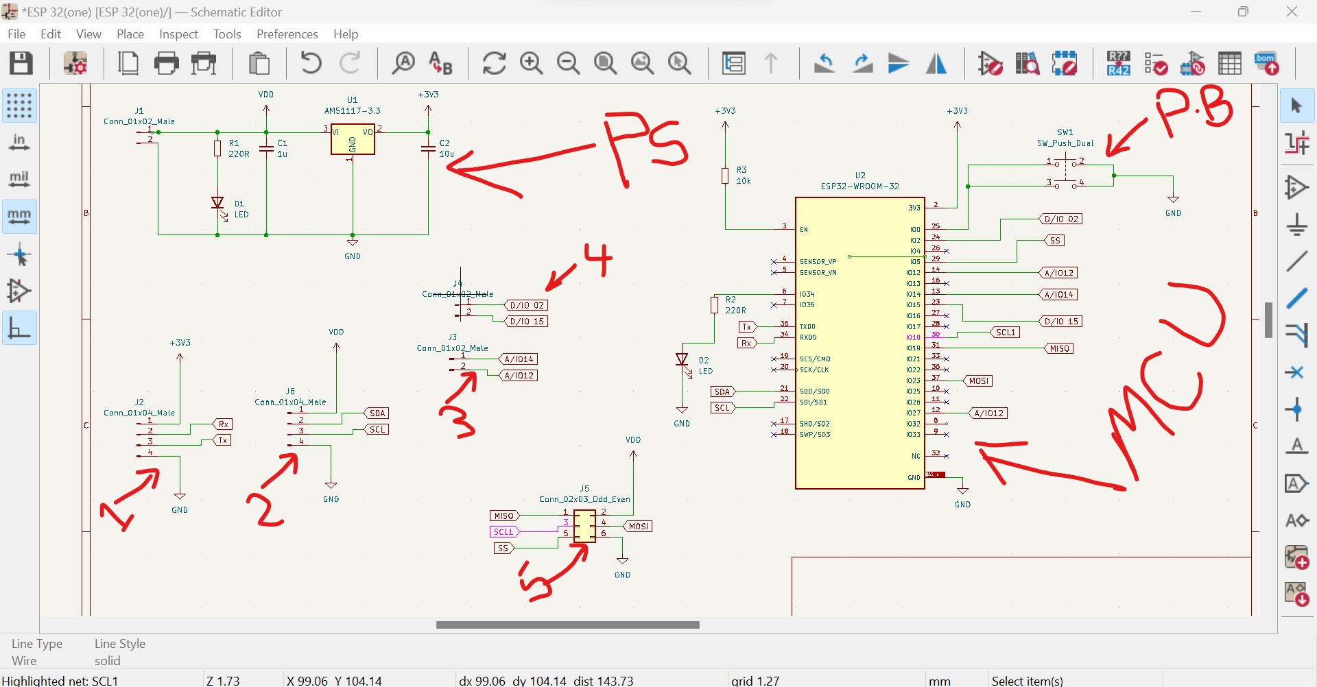
The schematic design includes the power supply circuit, crystal oscillator, reset circuit, programming and debugging interfaces, and other essential components as shown in the diagram below: - 3. Once the schematic design is complete, the next step is to create a PCB layout design for the development board.
The layout design includes placing the components on the board, routing the traces, and ensuring proper clearance and alignment. - 4. Prototype the development board to ensure that it works as expected. Verify the board's functionality by programming the microcontroller and testing its various features.
- 5. After completing the prototyping phase, proceed to the production phase. Fabricate the PCBs, assemble the components, and test the final product to ensure that it meets the required specifications.
- 6. Programming and Debugging: The development board requires a software toolchain, including a compiler, linker, and programmer, to program and debug the microcontroller. Ensure that the software toolchain is compatible with the microcontroller and the development board.
According to my project requirements, I used ESP32 Microcontroller to be used.
ESP32 is a low-cost, low-power system-on-a-chip (SoC) microcontroller with integrated Wi-Fi and Bluetooth capabilities. It is designed and manufactured by Espressif Systems and is popularly used in Internet of Things (IoT) applications and projects due to its wireless connectivity and advanced features. The ESP32 features a dual-core processor, which can operate at speeds of up to 240 MHz, and includes built-in support for Wi-Fi 802.11b/g/n and Bluetooth 4.2. Additionally, it has a large number of general-purpose input/output (GPIO) pins, analog-to-digital converters (ADCs), and other peripheral interfaces, making it highly versatile and adaptable to a wide range of use cases. The ESP32 is also highly programmable and can be programmed using a variety of programming languages, including C and Python, making it accessible to developers of different skill levels and backgrounds. Overall, the ESP32 is a powerful and flexible microcontroller that is ideal for a variety of IoT and embedded applications.
Milling, stuffing, and soldering a printed circuit board (PCB)
Milling: Milling involves using a CNC machine to cut a PCB out of a blank copper-clad board. This process requires a CAD software to create a design file of the circuit board, which is then loaded into the CNC machine. The machine will use a small cutting tool to cut the board according to the designed file.
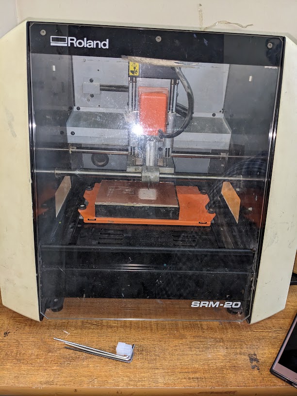
In my work I used The Roland SRM-20 as shown in the following picture:
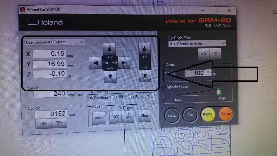
The SRM-20 comes with VPanel software, which allows for easy setup and operation of the machine. The software also includes features for toolpath generation, cutting simulation, and more.
It should be connected to a computer using a USB cable, making it easy to transfer files and control the machine.
Here are the steps I followed to set the origin of the machine before milling my PCB:
- 1. Open the Roland SRM-20 software, VPanel
- 2. Load the Gerber files into VPanel by selecting "File" "Import" and selecting the relevant files
- 3. Once the files are loaded, select "Layout" in the "Model" section of VPanel
- 4. Place the end mill (milling bit) at the starting point for milling on the PCB
- 5. Use the X, Y, and Z axes in VPanel to move the end mill to the exact position that you want to set as the origin point for milling
- 6. The origin point is now set, and the next is begin milling the PCB
Stuffing: Once the board is milled, the components can be inserted into the board's through-holes or surface-mount pads with the following steps:
A.Here I gathered the components required for the PCB and ensure that they are correctly identified,and even Check if the components are not damaged or defective.
B.Identify the location of each component on the PCB
C.Begin inserting the components into the board's through-holes or surface-mount pads in right way
D.Once all components have been inserted, double-check the placement of each component to make sure they are in the correct location, and in the correct orientation
E.Inspect the board for any bridging or short circuits between adjacent pads that may cause malfunction
F.Once you have confirmed the location and orientation of all the components, apply solder to the pads of through-hole components or surface-mount pads of SMD components to create a strong and durable connection
G.Clean the board with a suitable solvent to remove any excess flux or residue from the soldering process
Soldering: Soldering involves heating up the solder on the component and the PCB pads to create a solid connection. This can be done using a soldering iron or a reflow oven. It's important to use the correct type of solder for the application, and to ensure that the solder joints are strong and free from defects.
Soldering is a process of joining two metal components using a filler metal called solder. Here are the basic steps involved in soldering:
- 1. Clean the metal surfaces to be joined using a wire brush or sandpaper to remove any rust, dirt, or debris
- 2. Heat the metal surfaces using a soldering iron, torch, or hot air gun until they reach the melting point of the solder
- 3. Apply the solder to the joint, allowing it to melt and flow into the joint by capillary action. The solder should be applied to the heated joint, not directly to the soldering iron.
- 4. Allow the joint to cool and solidify. Do not move the joint or disturb it until it has completely cooled
- 5. Clean the joint with a brush or cloth to remove any excess flux or solder residue
- 6. Inspect the joint for any signs of cracking, voids, or other defects. If necessary, reheat the joint and add more solder to fill any voids
Design and Production of a Microcontroller programmer
A microcontroller programmer or microcontroller burner is a hardware device accompanied with software which is used to transfer the machine language code to the microcontroller/EEPROM from the PC
As I will need my Microcontroller to communicate with my Personnel computer or to be programmed through it, I have to produce also a programmer that will help me to load the instuctions into microcontroller from my computer.
I chose to use ESP32 due to its advantages, The ESP32 is the successor to the ESP8266. It adds extra CPU cores, faster Wi-Fi, more GPIO, and supports Bluetooth 4.2 and Bluetooth Low Energy.
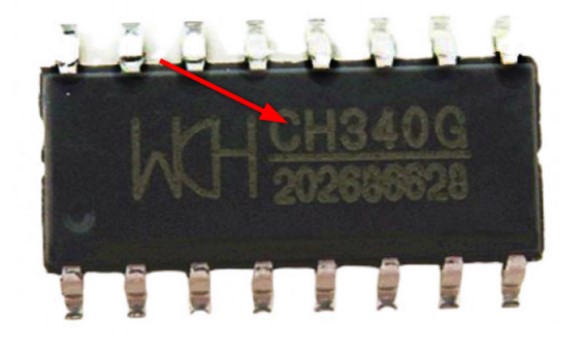
CH340G programmer for ESP32
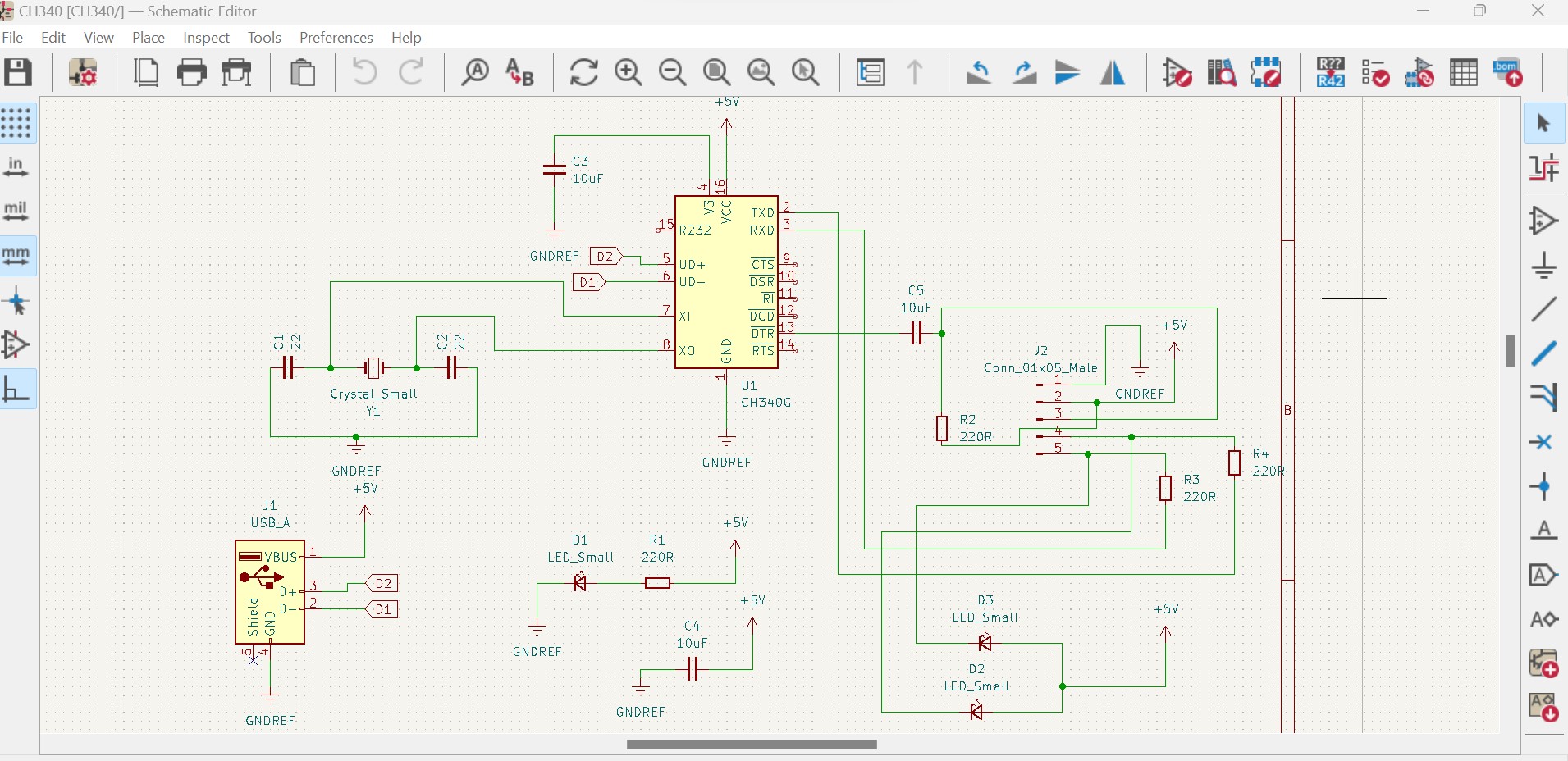
The device is built around cheap and popular CH340G chip,ESP32 is a microcontroller board and to communicate with a PC, ESP32 has onboard USB to UART bridge. Using this ESP32 can receive instruction from all UART devices. To establish this communication CH340 chip is used and before we can set up ESP32 with the PC the chip drivers must be installed in the PC.
Steps to Install Serial Drivers for ESP32 CH340 Chip:
1: ESP32 CH340 USB to UART Bridge:USB to UART is like a language translator that converts one set of information to an other. It interfaces two devices to exchange information and data. USB to UART is used in microcontroller boards like Arduino, NodeMcu, ESP32 and ESP8266. Using CH340 chip serial communication is established between PC and microcontroller.Most of the boards including ESP32 uses CH340 for UART communication.
2: How to Identify ESP32 Boards UART Chip:The first and simple step to identify the chip name is by reading it over the chip itself. Most of the time model numbers are written on chips. And most of these chips have the same package file.
3: How to Check ESP32 Drivers Installed or Not:To check drivers’ installation, we can use two different methods:Using Arduino IDE or Using Device Manager
3.1: Using Arduino IDE:Connect the ESP32 with the PC and open Arduino IDE then go to Tools>Port. If the drivers were not installed the port option will be grayed out.
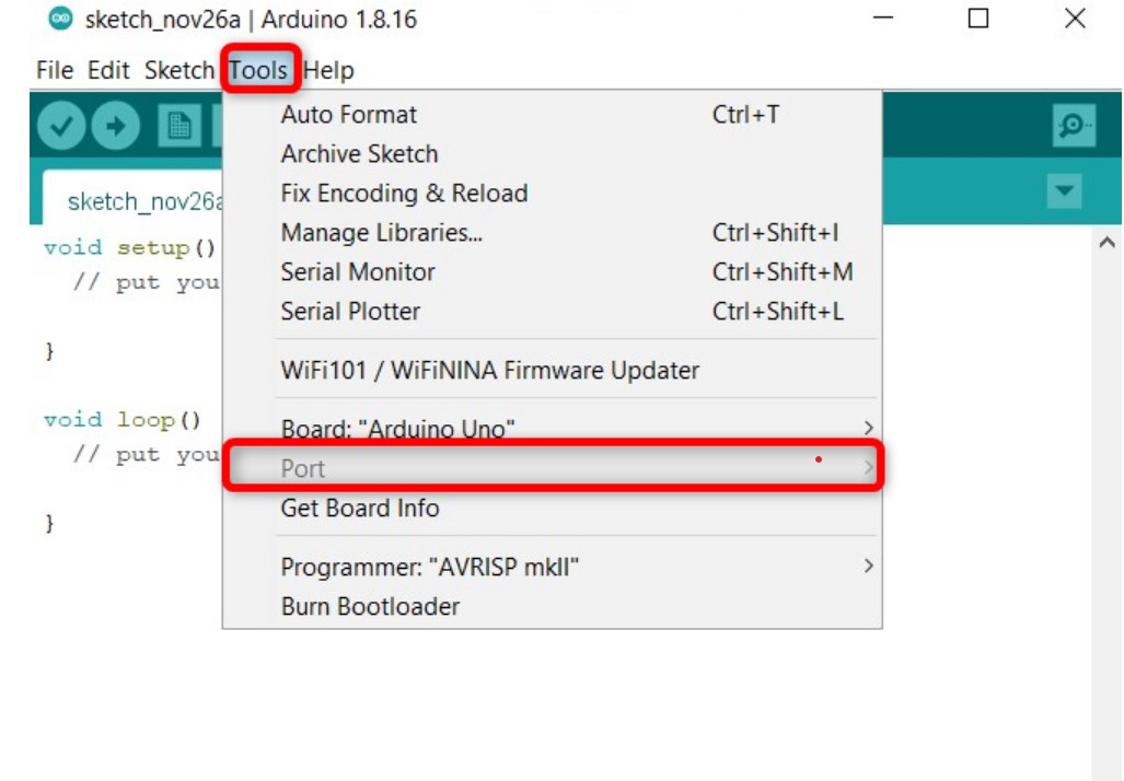
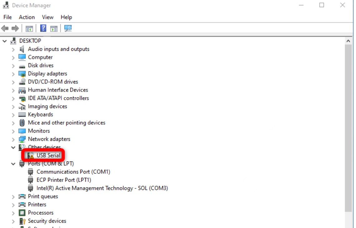
3.2: Using Device Manager:Another way of checking ESP32 drivers is connect ESP32 with PC and open Device Manager then search for the drivers under devices or COM & LPT section. If the drivers were not available a yellow warning symbol can be seen.
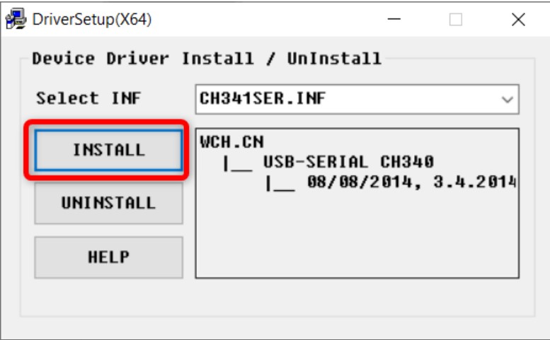
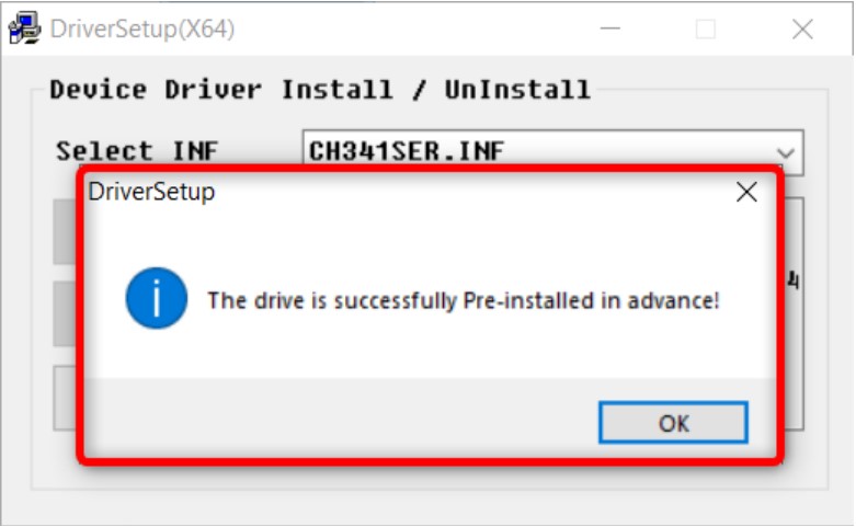
4: Installing CH340 Drivers for ESP32 in Windows:
For serial communication between PC and ESP32 UART drivers are needed. To install ESP32 drivers, first connect the board with the PC.
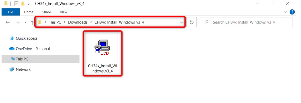
Step 1: Download drivers from https://www.wch.cn/downloads/CH341SER_ZIP.html

Step 2: After download is finished unzip the drivers file into a new folder. Double click to open the installation file.
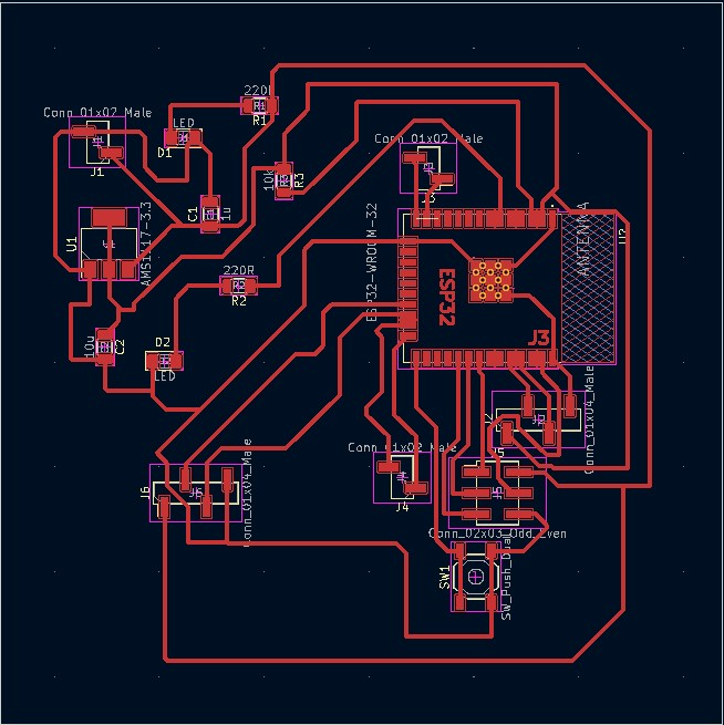
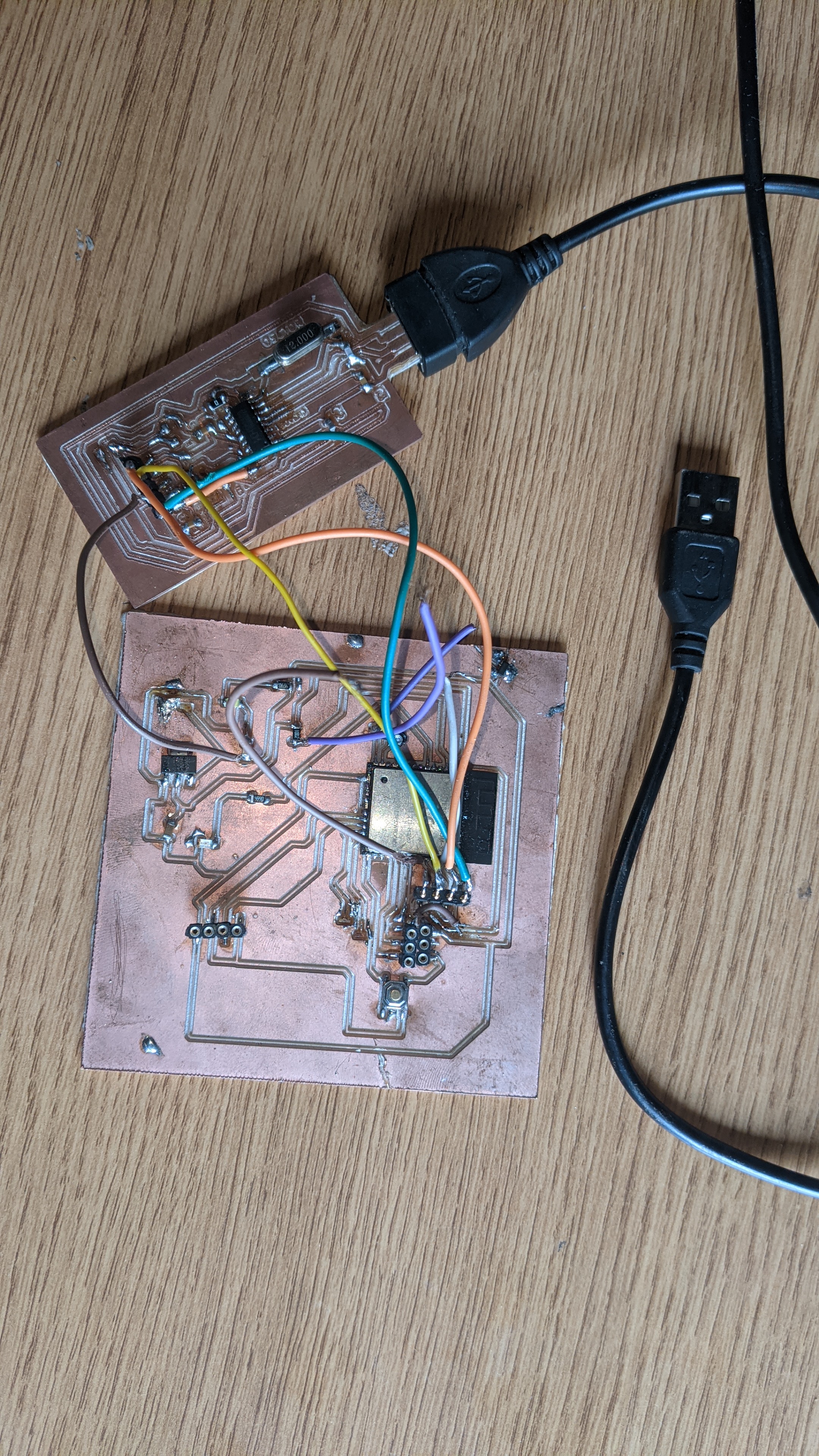
Design of CH340 to ESP32 programmer
The bellow designs have been done by using Kicad.
Schematic Design:
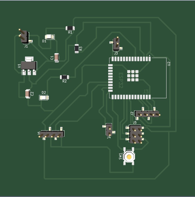
PCB Design:
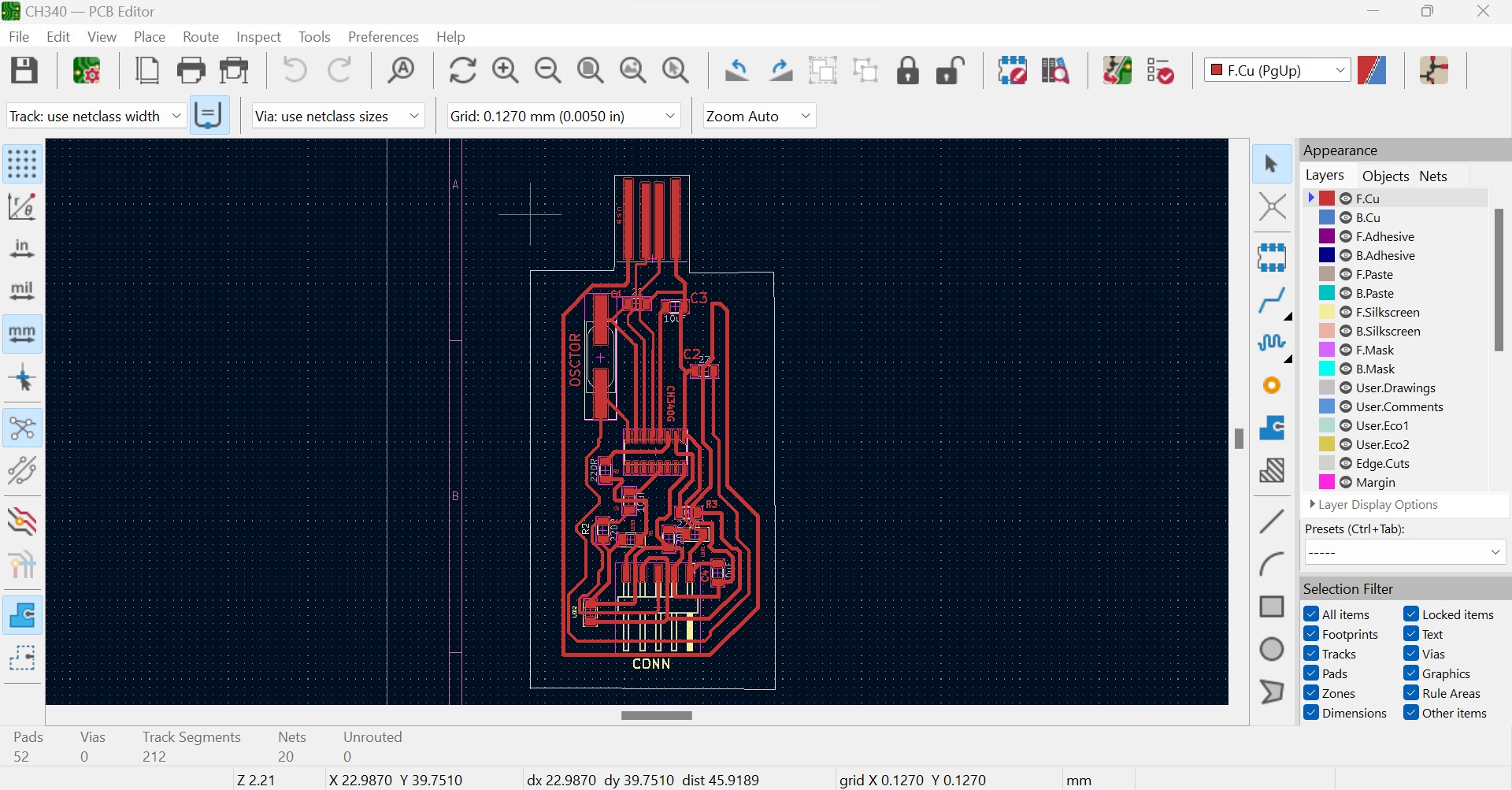

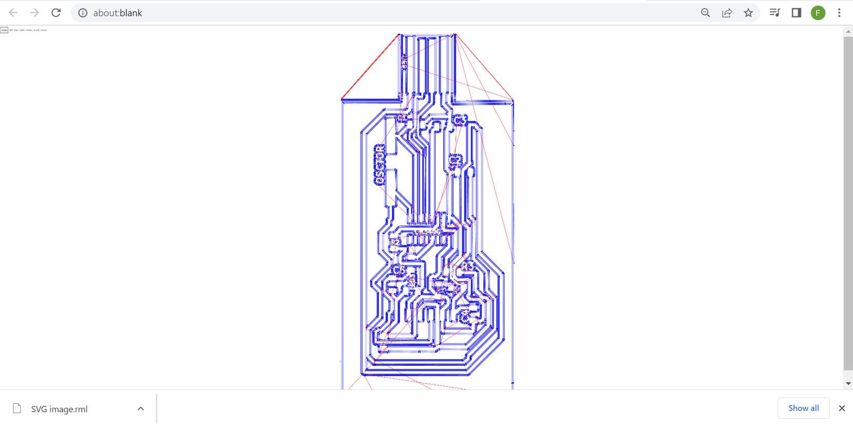
Converting the designed PCB into G-code to be cutted by milling machine
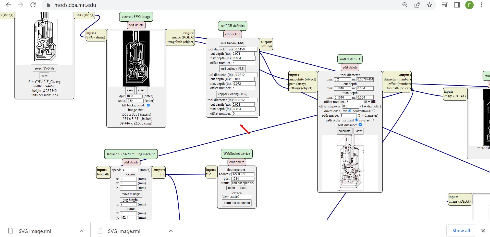
After converting designed pcb into G-code:
Then down here there is a produced PCB after milling:
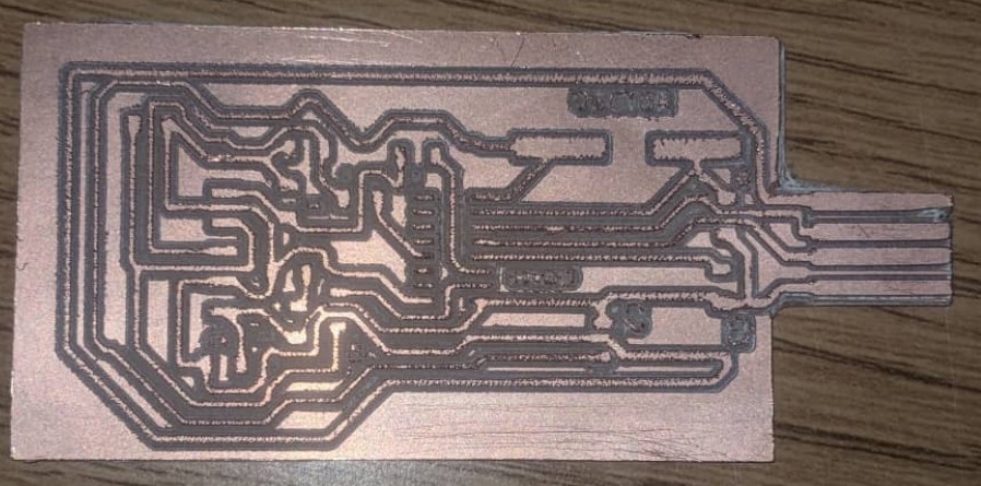
Image: Final pcb of programmer
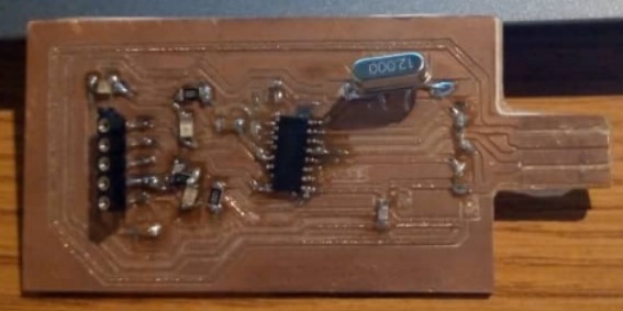
After soldering the components on the board and checking any mistake done by using multimeter, I connected it on my computer to in order to be sure that it is working

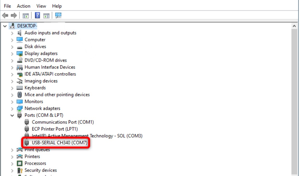
Step 5: To check whether the driver is installed or not you can confirm it by opening Device Manager and check the driver under COM & LPT section.
As you can see, my CH340 is connected on port COM6 which assure me that my board is well working.
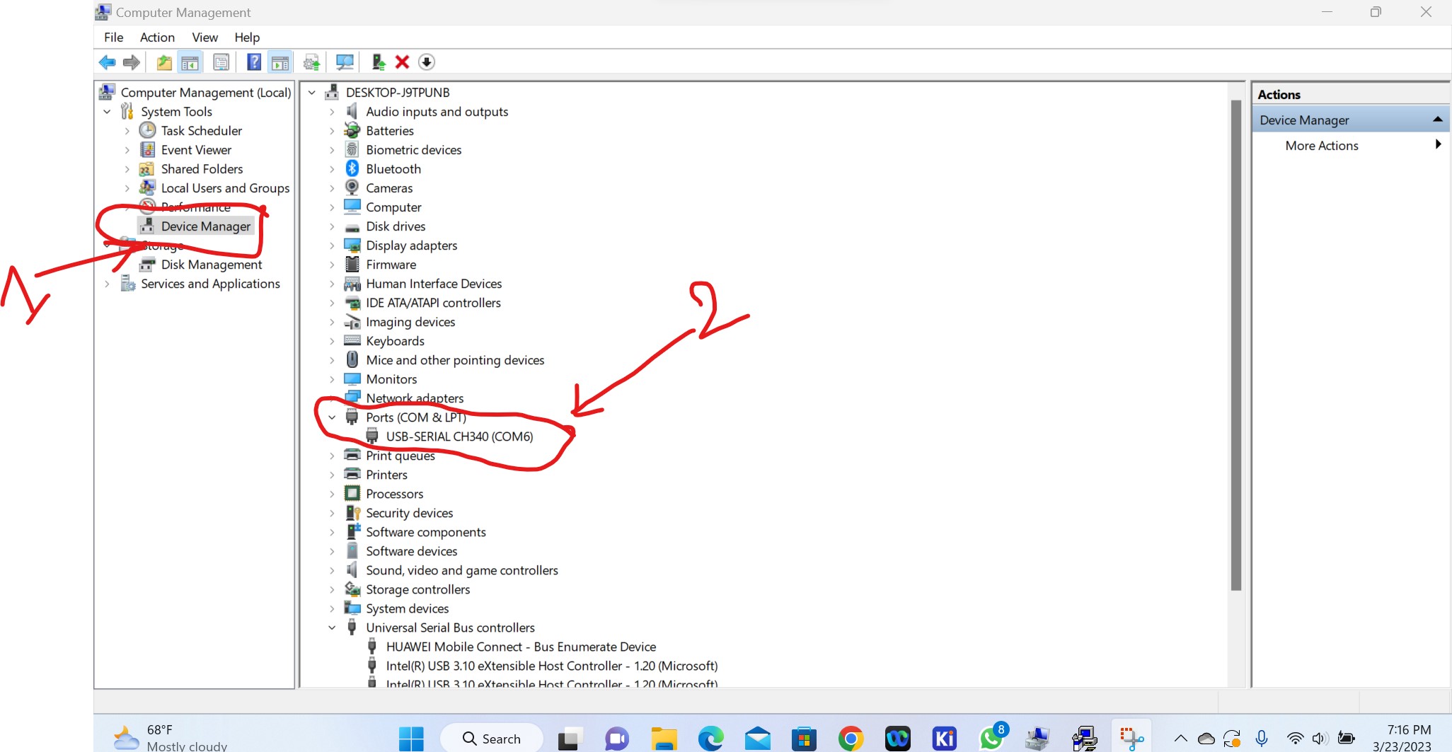
Image: Now the drivers are installed as shown in above photo
Testing my programmer

To test if my programmer works I just used it to program an ESP32 board. As shown by image and the following video, I just uploaded the simple codes to count from zero to 1000 into ESP32 board by using my CH340 programmer:
      int a;
void setup() {
Serial.begin(9600);
}

void loop() {
for (a = 0; a<= 1000; a++){
  Serial.println(a);
  delay(700);
}

}
As I have designed a programmer that should be connected on the port of computer, the head of my board is some how small on the down side to fit well in the port of computer, What I did is to support it with any piece of material on that side as it can't cause the short circuit because that side doesn't have any connection(as my pcb is single sided).
The files including SVGs can be downloaded via here