Electronics Production
Assignment activities:
Group assignment:
Characterize the design rules for your in-house PCB production process
extra credit: send a PCB out to a board house
II.Group Assignment:
If you want to explore the group Assignment Click
Here
PCB design rules refer to a set of guidelines and specifications that dictate how a printed circuit board (PCB) should be designed to ensure it functions properly and can be manufactured efficiently and cost-effectively. Here are some common PCB design rules:
Reference
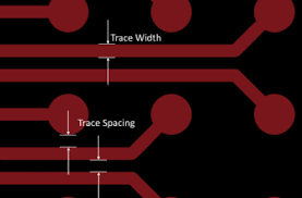
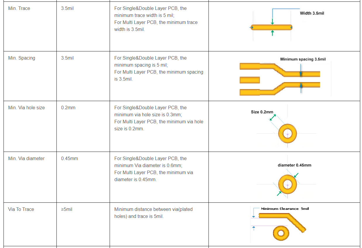 1.Trace width and spacing:
These rules define the minimum width and spacing required for the traces on the PCB. The width of the traces determines their current carrying capacity, and the spacing helps prevent electrical interference and arcing between traces.
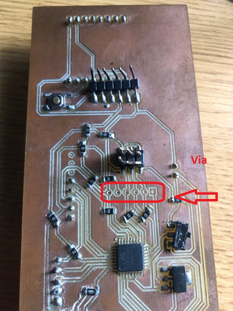
 2.Via design:
Vias are used to connect different layers of the PCB together. Via design rules define the minimum size and spacing requirements for vias, as well as the minimum distance between vias and other PCB features.
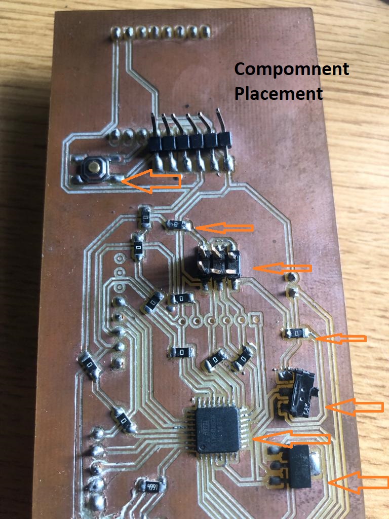
 3.Component placement:
Components should be placed in a way that minimizes electrical interference and maximizes signal integrity. This involves considering the location of sensitive components, such as high-speed devices, and ensuring they are placed away from noisy components like power supplies and motors.
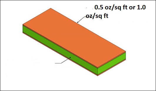
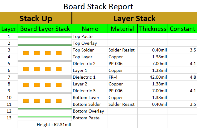
 4.Copper thickness:
Copper thickness affects the current carrying capacity of the PCB. Design rules should specify the minimum and maximum copper thickness for different layers of the PCB.
Reference on Copper Thinkness
Individual Assignment
Designing a programmer that interacts and communicates with an embedded microcontroller, such as the CH340, involves the following steps:
The 1st step we choose communication protocal Determine the communication protocol: Decide on the communication protocol that will be used to communicate between the programmer and the microcontroller. In this Assignment we prefer to use
UART as communicatio Protocol.
What is UART?: UART stands for Universal Asynchronous Receiver/Transmitter. It is a type of serial communication protocol that is commonly used to communicate between microcontrollers, sensors, and other embedded devices.
UART is a half-duplex protocol, which means that data can only be transmitted in one direction at a time. However, because it is asynchronous, there is no need for a clock signal to be transmitted along with the data. Instead, the transmitter and receiver agree on a common baud rate (the rate at which data is transmitted) and the number of data bits, stop bits, and parity bits in each message.
In UART communication, data is transmitted as a series of bits. Each message is typically structured as a sequence of start bits, data bits, optional parity bits, and stop bits. The start bit is used to signal the beginning of a new message, while the stop bit is used to signal the end of the message.
UART is a simple and widely used communication protocol that is supported by most microcontrollers and embedded devices. It is often used in applications where low data rates are sufficient, such as in control systems, data acquisition, and monitoring applications.
If you want to read more about UART Click Here
2nd Step we Choose Microcontroller: Select the microcontroller that will be used in the programmer. Ensure that it is compatible with the communication protocol chosen in step 1 and has sufficient processing power and memory to perform the required tasks. In this Assignment we prefer to use
CH340
What is CH340? CH340 is a USB to serial converter chip that is commonly used in embedded systems to provide a USB interface for communication with a microcontroller or other device. The chip is manufactured by WCH, a Chinese semiconductor company.
The CH340 chip provides a low-cost, simple way to add USB connectivity to embedded systems that do not have native USB support. It is often used in applications such as Arduino and other microcontroller-based projects.
The CH340 chip supports several standard communication protocols, including UART, I2C, and SPI, and is compatible with a wide range of operating systems, including Windows, Linux, and Mac OS X. It operates at speeds of up to 2 Mbps and is designed to be low-power, making it ideal for battery-powered devices.
The CH340 chip is available in several different package types, including SSOP-20, SOP-16, and DIP-16, and is widely available from electronics suppliers and distributors. Its low cost and ease of use make it a popular choice for hobbyists and professional engineers alike.
If you want to read more about CH340 chip Click Here
3rd we choose Components required:
- 1.Ch340g
- 2. 12MHz crystal
- 3. 1k resistors
- 4. 100nf capacitors
- 5. 0805 package led
4th Step Design the schematic: Create a schematic diagram that shows the connections between the components in the programmer circuit. This includes the microcontroller, the CH340 USB to serial converter chip, and any other components such as LEDs or buttons.
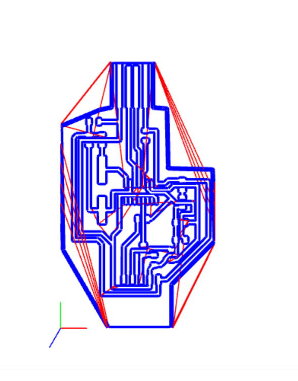
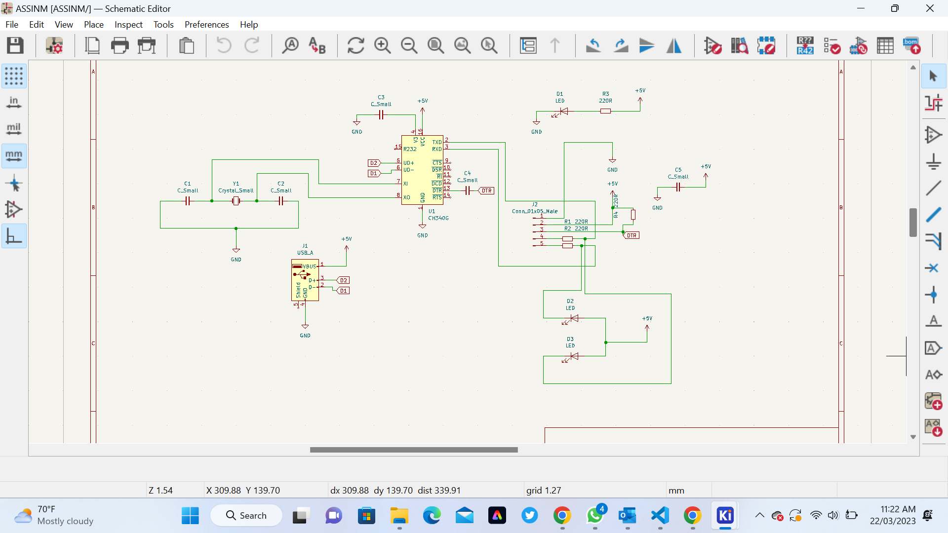 5th Step Create a PCB layout
: Using KiCad or another PCB design tool, create a PCB layout based on the schematic diagram. This involves placing the components on the board and routing the traces that connect them.
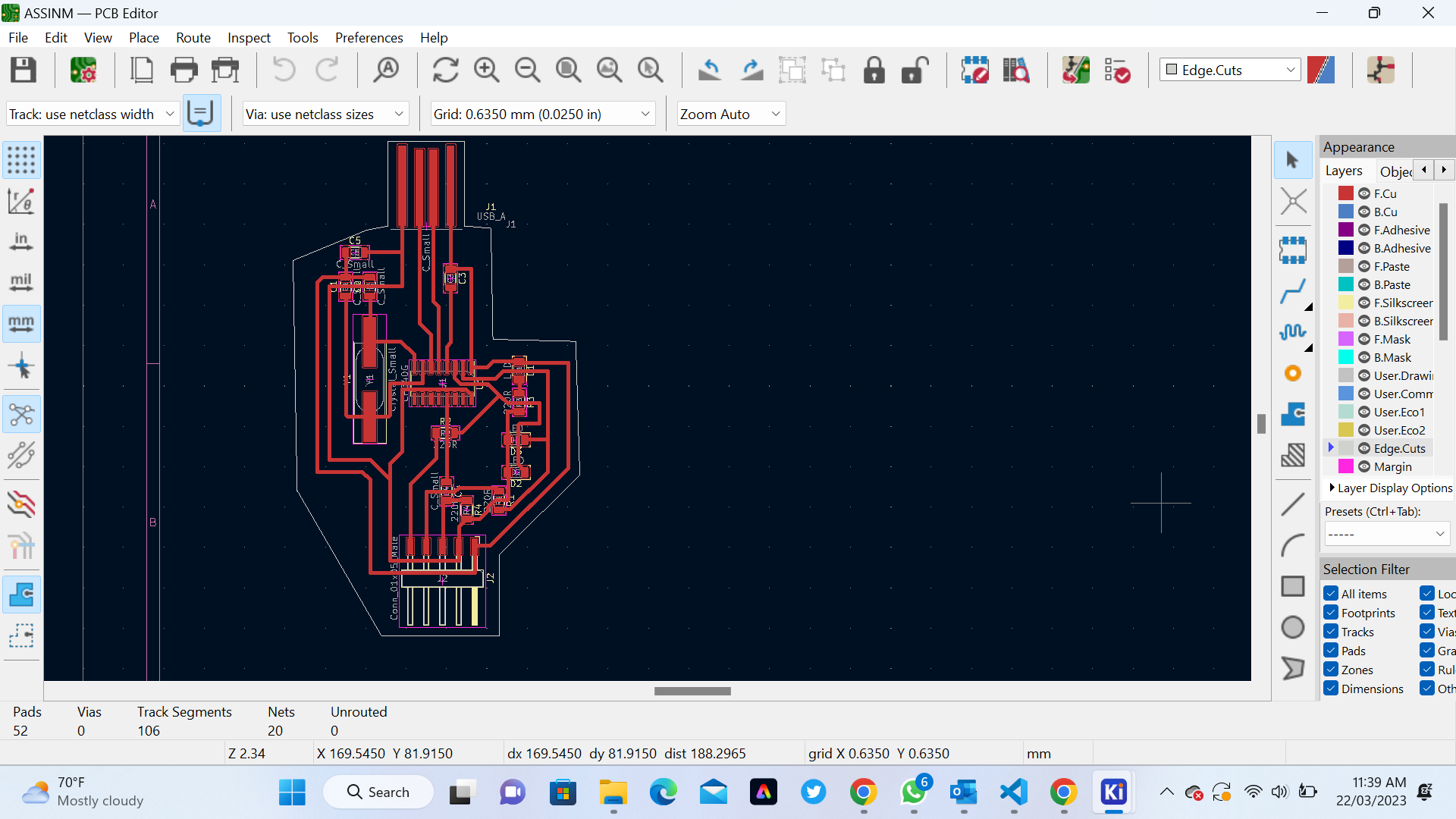 6th Step Generate Gerber files:
 Once the PCB layout is complete, generate Gerber files that can be used to manufacture the PCB. These files include information on the size and placement of the components, the routing of the traces, and other details needed to create the PCB.
We used this Module
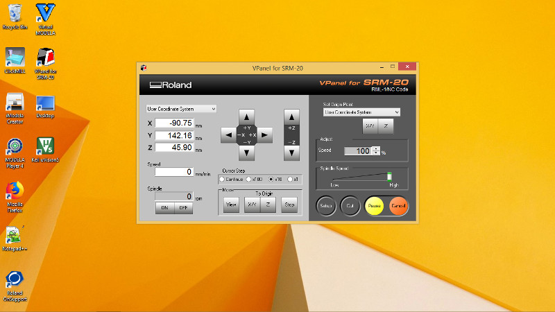
After downloading the .rml file, we have to import it in the VPanel for SRM-20 software in order to trace it. Here I had to first set the XYZ axes positions:
After I prepare for Taping PCB Board
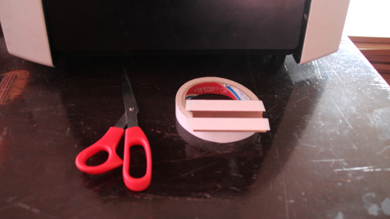
Next, I fixed it to the sacrificial board that is fixed on the machine bed:
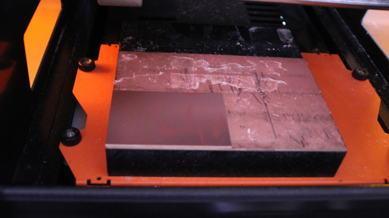
To mill a PCB, you will need a CNC milling machine (Roland MonoFab SRM-20) that is capable of handling PCBs and The software will generate the necessary G-code instructions to control the CNC machine.
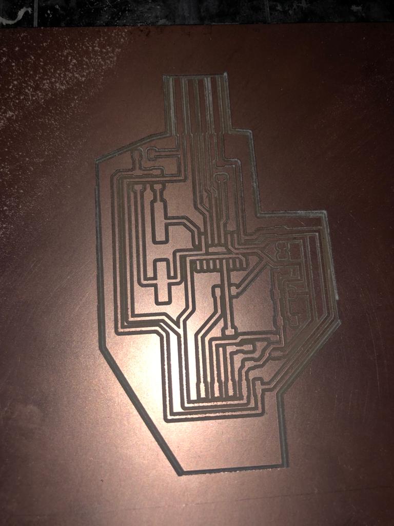
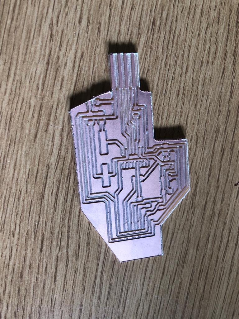
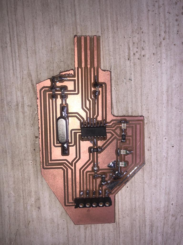
This is my PCB after milling
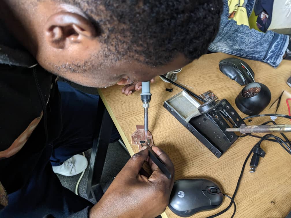
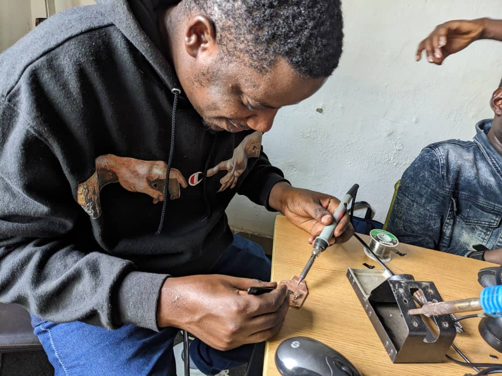
Here I started soldering Components to PCB
Here is the final result after soldering:
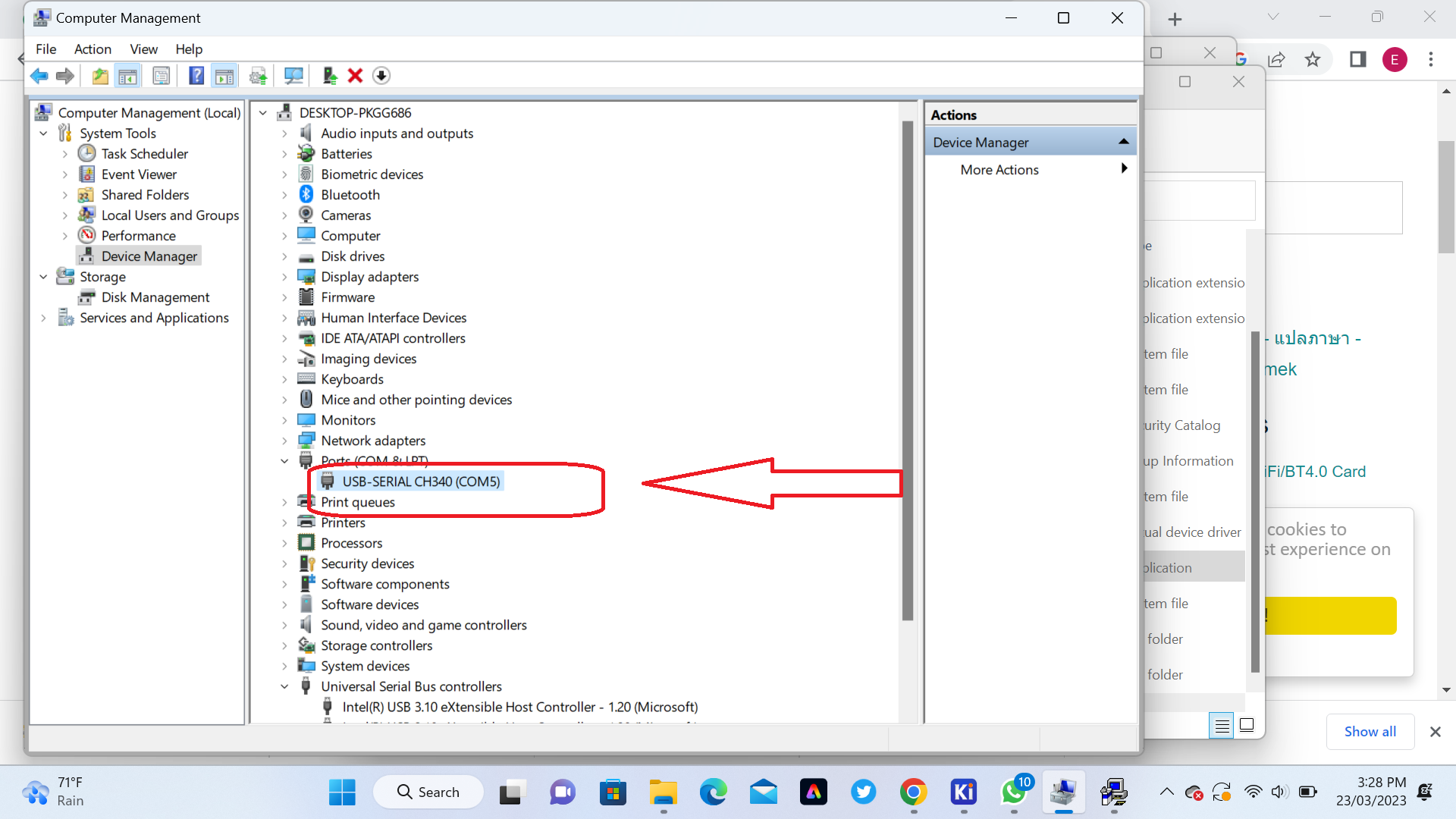
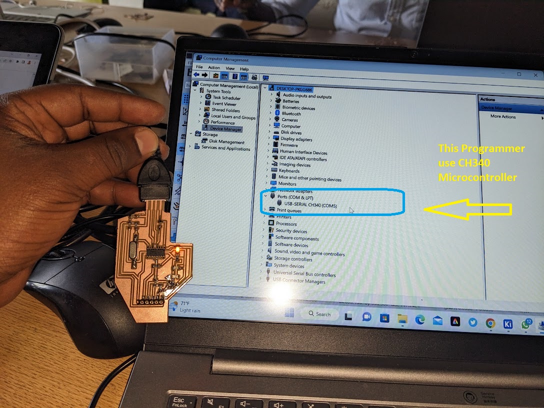
We connect Computer and our Programmer (Ch340G) but unfortunately its drivers not updated, we update these drivers as shown on following screen shots
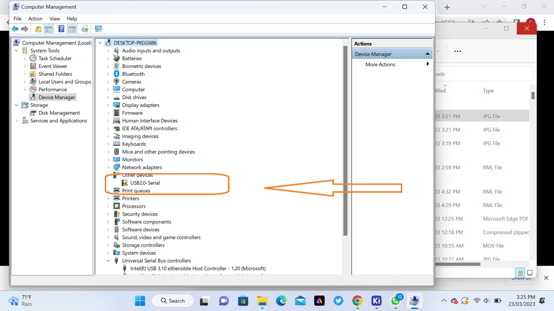
The next task was to download and install
Ch340G drivers on this link
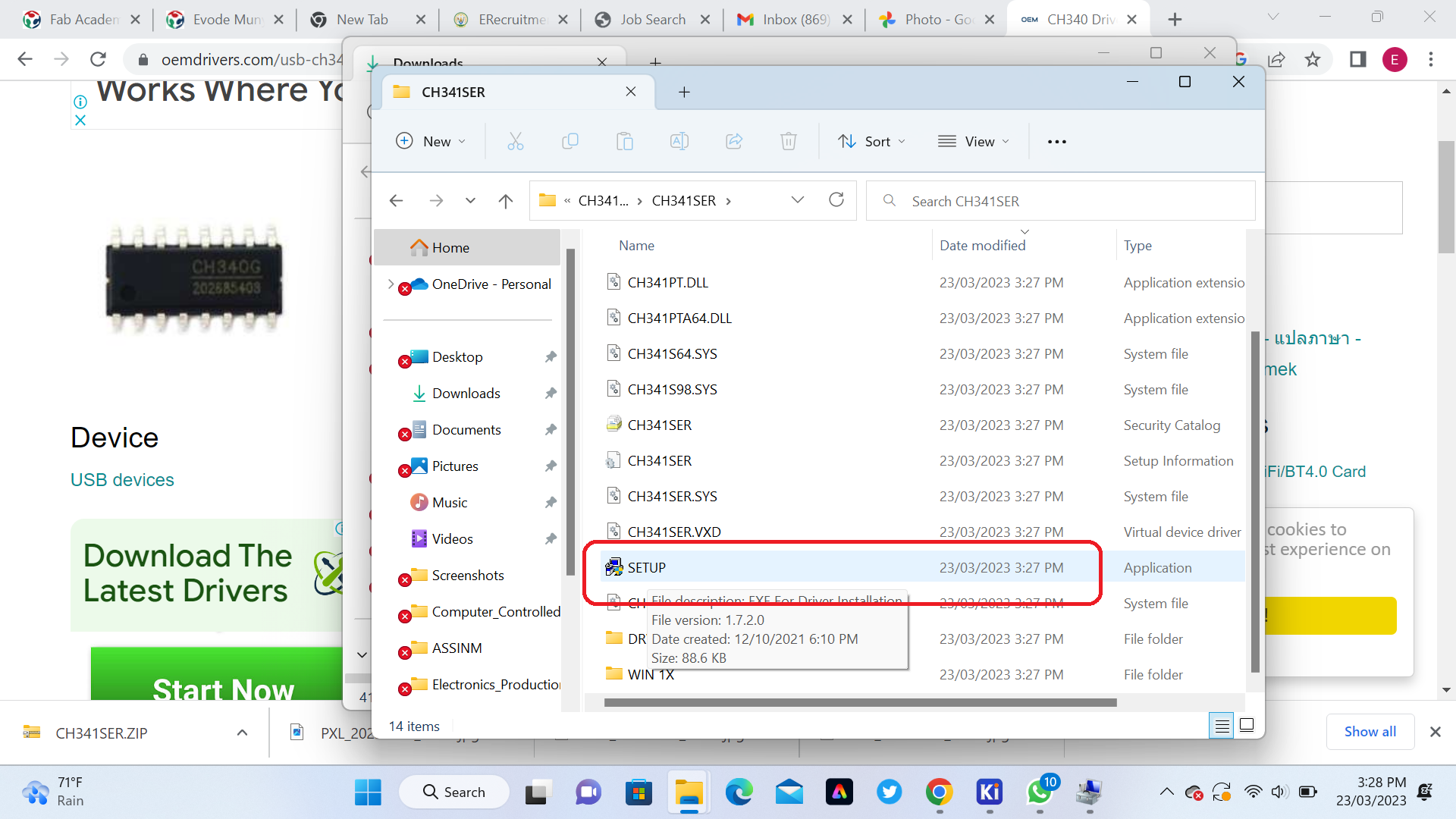
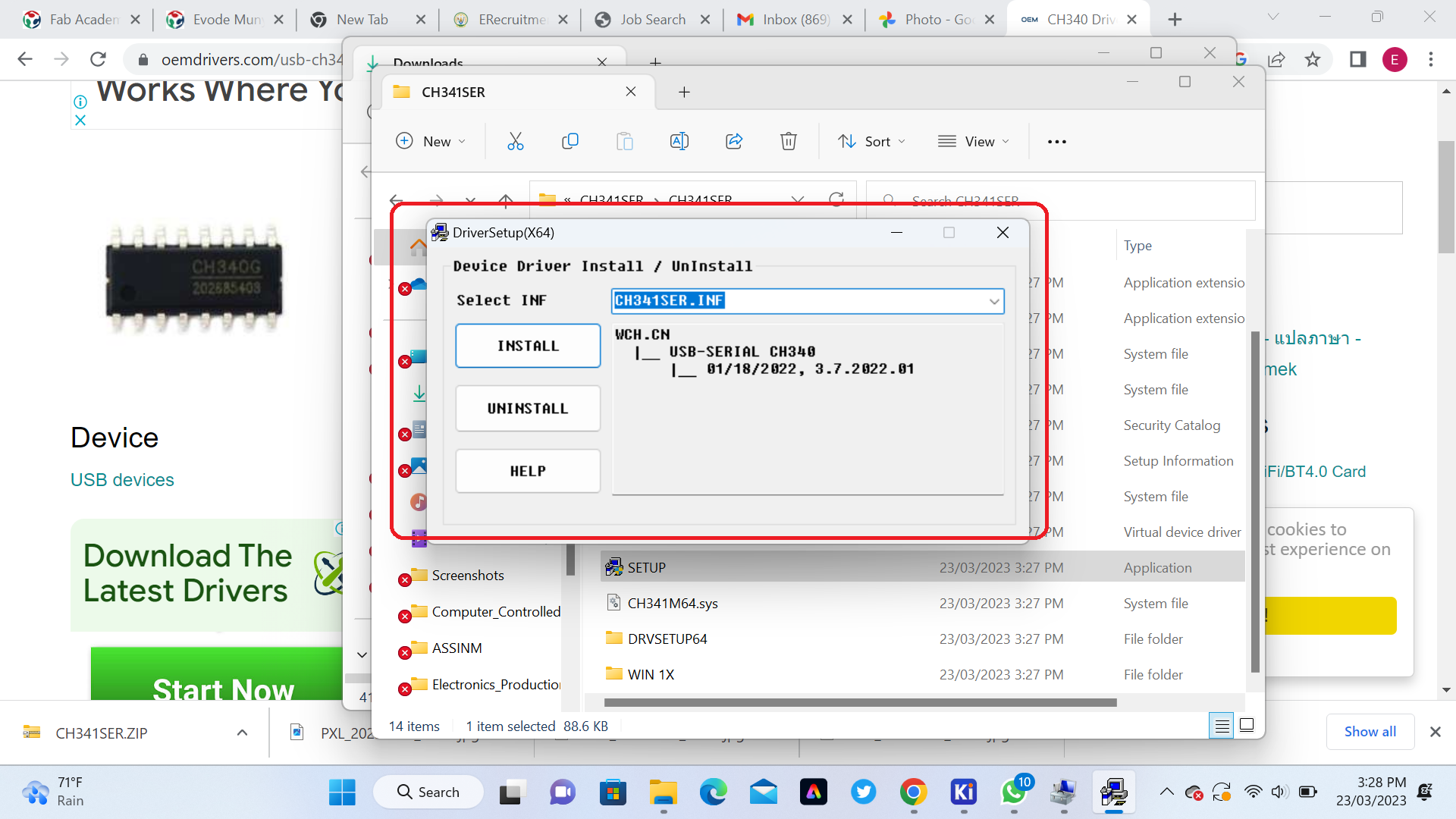
Now the drivers was updated as shown on below Screenshot
Wowwwwwwww Here is my programmer connected to my Computer
.jpg)
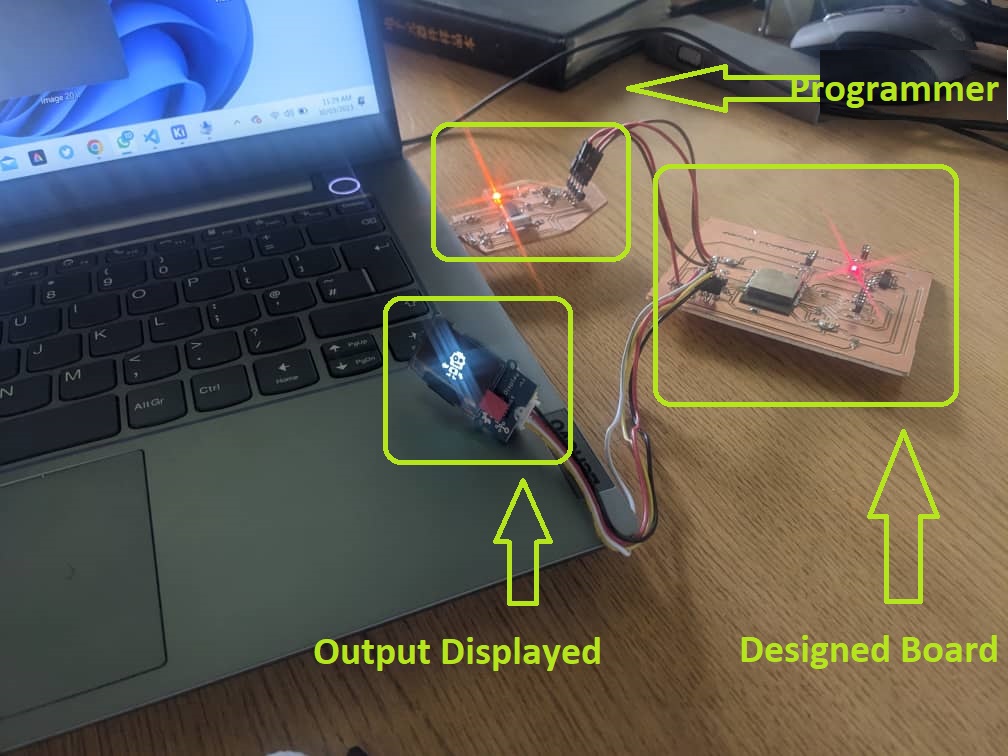
 By using a Programmer upload Arduino code which diplay image of robot, This board used in this image was designe in Output Week Here is a picture of my output which display an image in OLED Screen
// Include the correct display library
// For a connection via I2C using Wire include
#include "DFRobot_OLED12864.h"

// Initialize the OLED display using Wire library
DFRobot_OLED12864  display(0x3c);

void drawLines()
{
  for (int16_t i=0; i=0; i-=4) {
    display.drawLine(0, DISPLAY_HEIGHT-1, DISPLAY_WIDTH-1, i);
    display.display();
    delay(10);
  }
  delay(250);

  display.clear();
  for (int16_t i=DISPLAY_WIDTH-1; i>=0; i-=4) {
    display.drawLine(DISPLAY_WIDTH-1, DISPLAY_HEIGHT-1, i, 0);
    display.display();
    delay(10);
  }
  for (int16_t i=DISPLAY_HEIGHT-1; i>=0; i-=4) {
    display.drawLine(DISPLAY_WIDTH-1, DISPLAY_HEIGHT-1, 0, i);
    display.display();
    delay(10);
  }
  delay(250);
  display.clear();
  for (int16_t i=0; i
If you want to learn about my designers,
kindly click here for downloading my files
1