Week 6: Electronic Design
Group assignment
Use the test equipment in your lab to observe the operation of a microcontroller circuit boardIndividual assignment
Design a development board to interact and communicate with an embedded microcontroller
Extra-credit: Try another design workflow
Extra-credit: Make a case for it and Extra-credit:Simulate its operation
Design of a development board to interact and communicate with an embedded microcontroller
KiCard is an open-source software suite for Electronic Design Automation (EDA) that allows users to design schematics and printed circuit boards (PCBs) for electronic circuits. It offers a range of tools for schematic capture, PCB layout, and 3D visualization, making it a popular choice among hobbyists and professionals alike.
A Printed Circuit Board (PCB) is a board made of insulating material with conductive pathways etched onto its surface, used for connecting and supporting electronic components. PCBs are essential for the construction of electronic devices and are widely used in various industries, from consumer electronics to aerospace and medical devices.
PCBs can be mounted on microcontrollers using surface-mount technology (SMT) or through-hole technology (THT), depending on the design and application requirements. SMT allows for smaller and more compact designs, while THT provides more secure connections for larger components and higher power applications.
A development board, also known as a prototyping board or a dev board, is a type of printed circuit board (PCB) designed for prototyping and testing electronic circuits and systems.
It typically contains a microcontroller, sensors, connectors, and other components that allow for easy experimentation with different hardware and software configurations. These boards often come with preloaded firmware or programming tools that allow developers to quickly start building and testing their projects.
Designing PCB
I am going to design a development board to interact and communicate with an embedded microcontroller like the Attiny45, and when the user press on the button indicated "1", the corresponding LED will blink until you release the button.
First thing: Download and install KiCad:
You can download KiCad from the official website from here and then Choose the appropriate version for the operating system and follow the installation instructions.
Launch KiCad:
Once the installation is complete, you can launch KiCad by clicking on the application icon in your program menu or desktop shortcut.
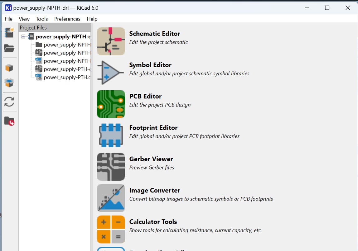
Create a new project: When KiCad launches, you will see the KiCad Project Manager. Click on "New Project" to create a new project. You will be prompted to select a project name and location.
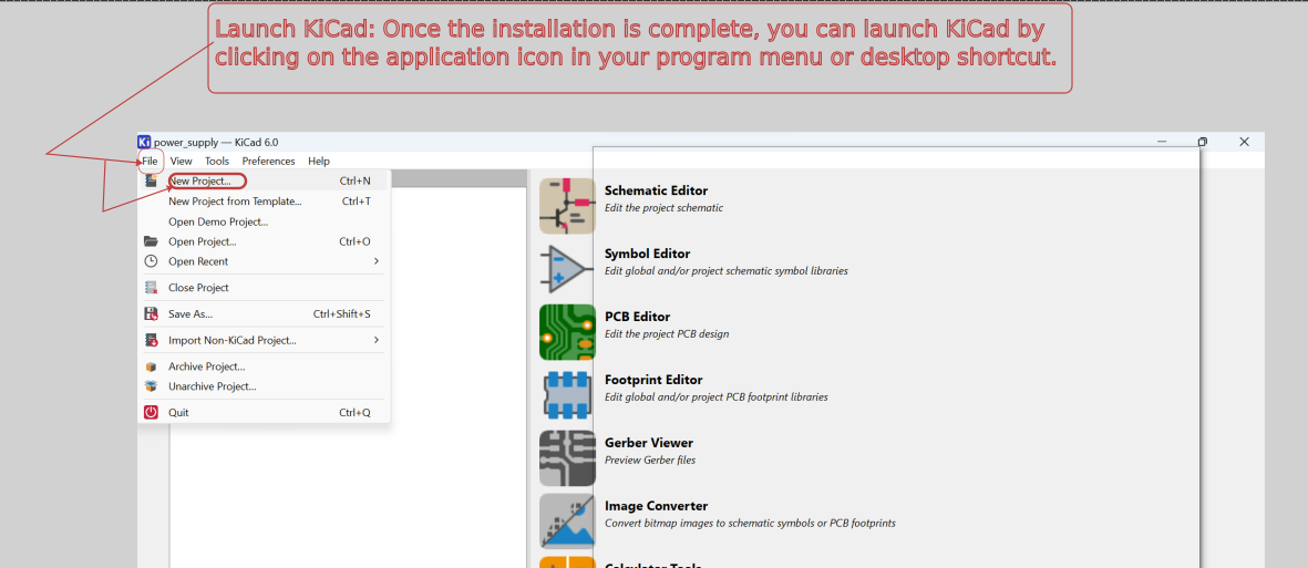
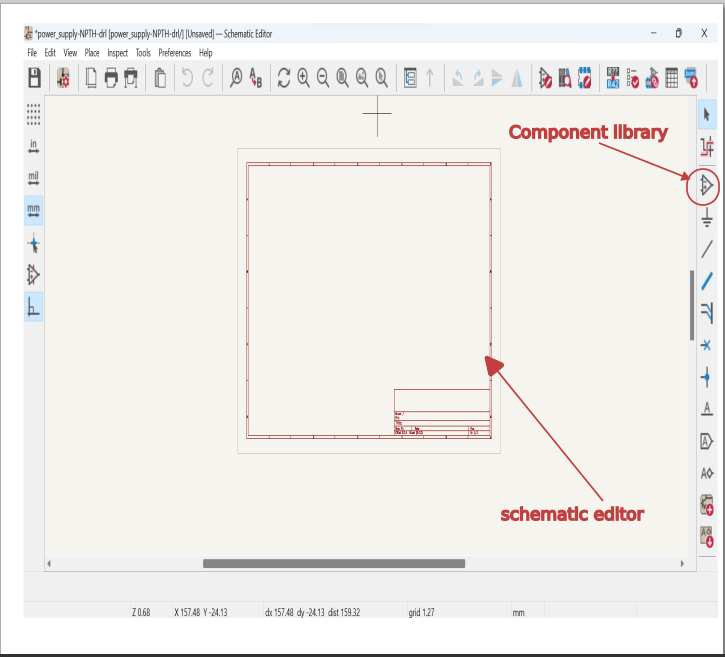
- Create new schematic by clicking on new, project, schematic; and
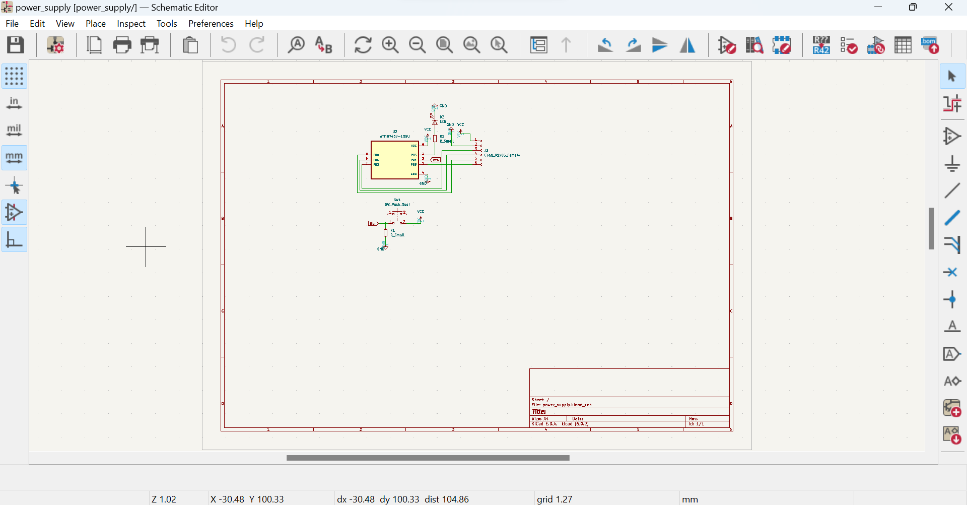
- Load the components into schematic editor and arrange them into the schematic diagram
Design the printed circuit board (PCB): Use the schematic diagram to design the PCB layout, placing and routing all the components on the board.
3D Model of the designed PCB:
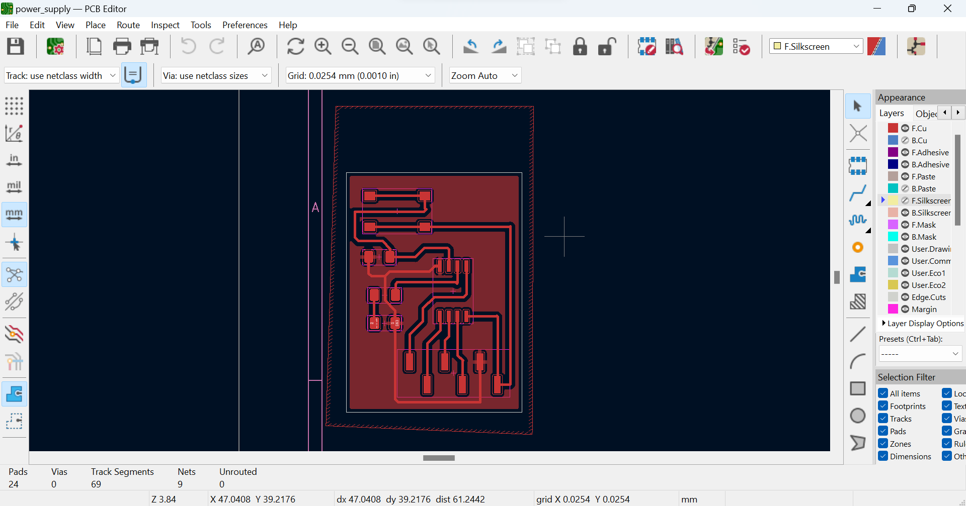
| From the above resulted PCB, I am going to fill all zones to ground (GND): |
|---|
| - Save image as SVG format to be processed for milling machine |
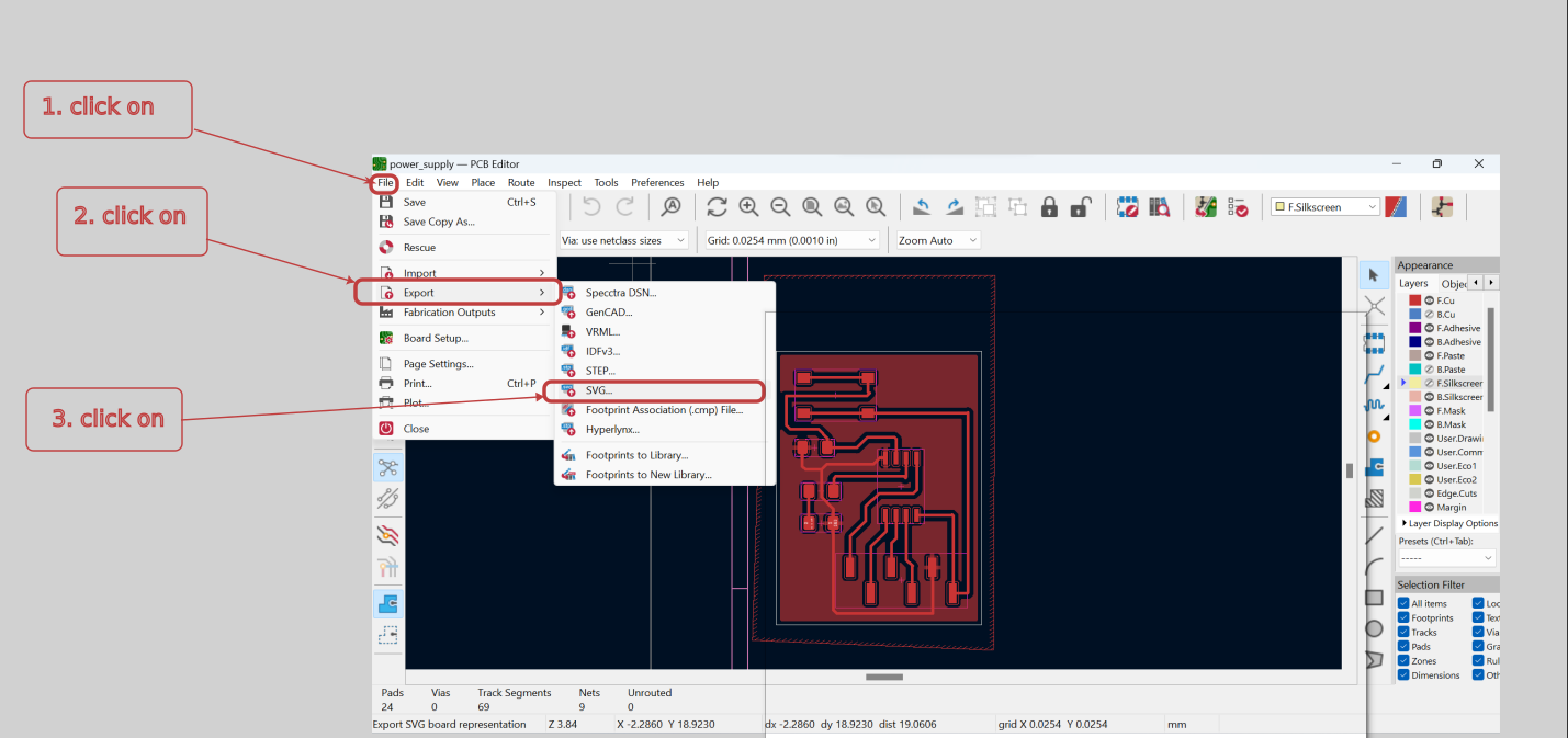
|
| - Export front layer and we set it in black and white including board edges |
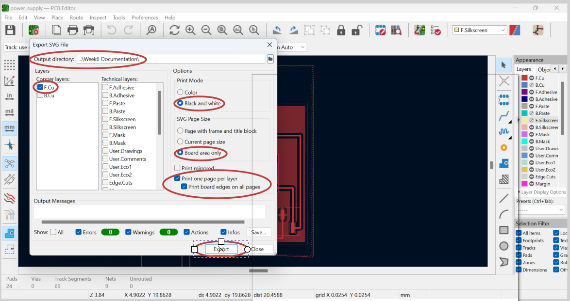
|
| - Below here is the exported SVG image opened in web browser |
After designing the board, move on to generate the Gerber files which are used to manufacture the PCB and they will be used to mill the board traces.
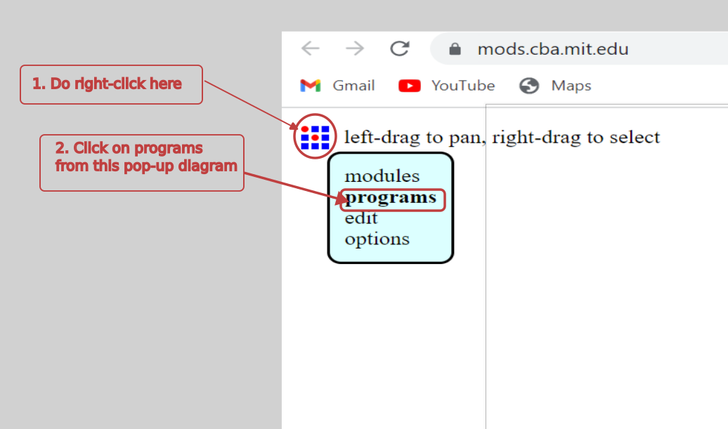
|
|
|
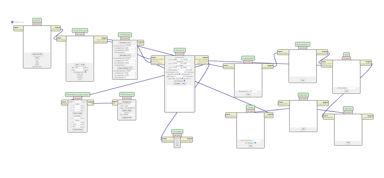 This interface allows you to set all the necessary parameters for the final file that the Roland CNC machine will use to create the traces on your PCB. |
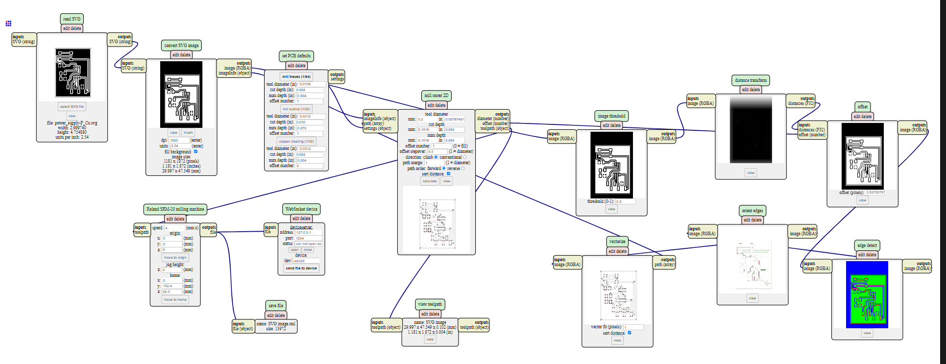 - In order to acquire the highest possible image resolution, set the DPI to 1000 and invert the image; - Choose the mill traces; - Set the offset number to any value you like for the CNC and the tool diameter; and - Do invert, so that the machine traces on the black area instead of the white one. |
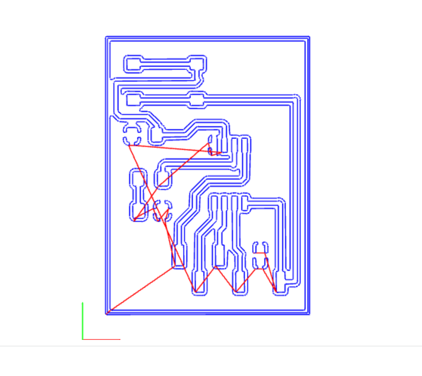 This is the produced tracing path that the milling machine will follow |
| Use Roland SRM-20 Milling machine |
|---|
|
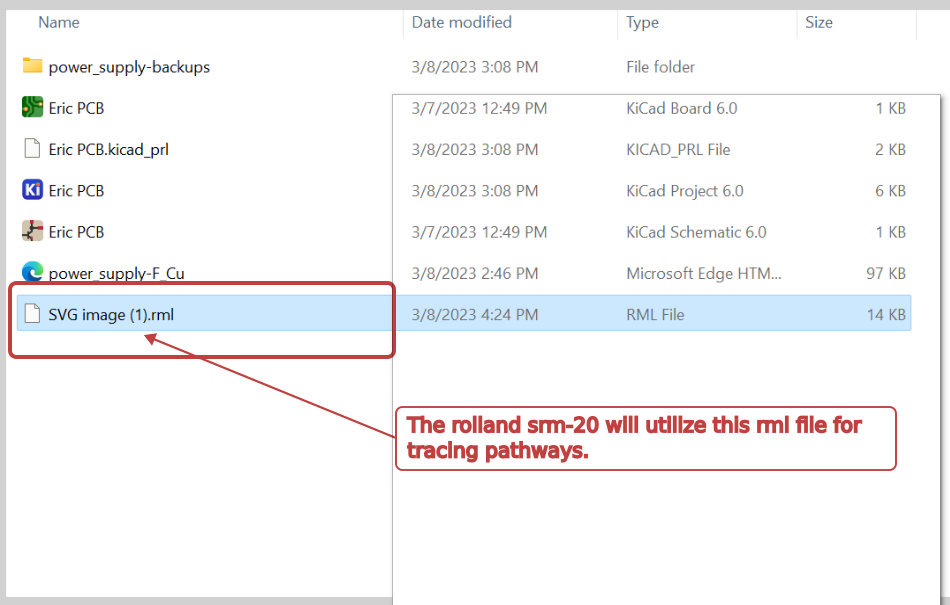
The Roland SRM-20 is a desktop milling machine designed for creating 3D models and prototypes from various materials such as plastics, woods, and metals. It has a compact size and user-friendly software, making it suitable for use in small workshops or labs. It offers high precision and accuracy, enabling users to produce intricate designs with ease.
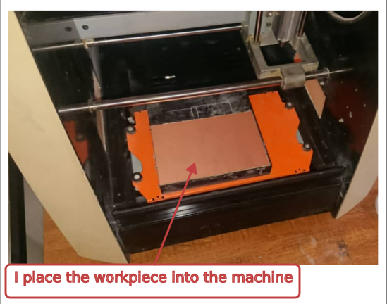
|
Load the design file: Load the design file into the milling software (e.g., Roland SRM-20's Virtual Modela) and set the cutting parameters (e.g., milling speed, depth, cut path).
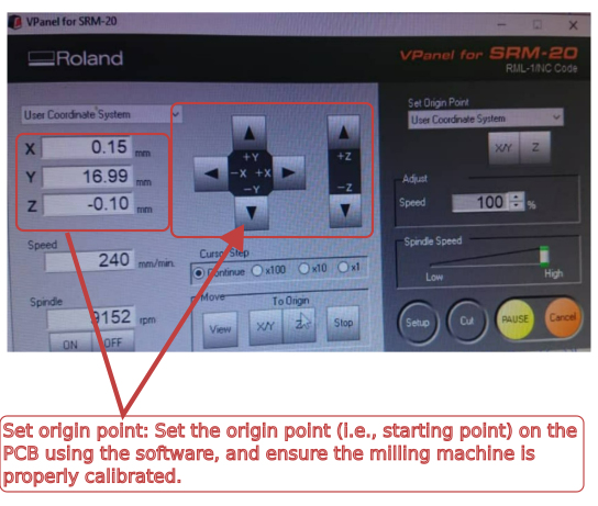
|
Here below is the flesh generated PCB 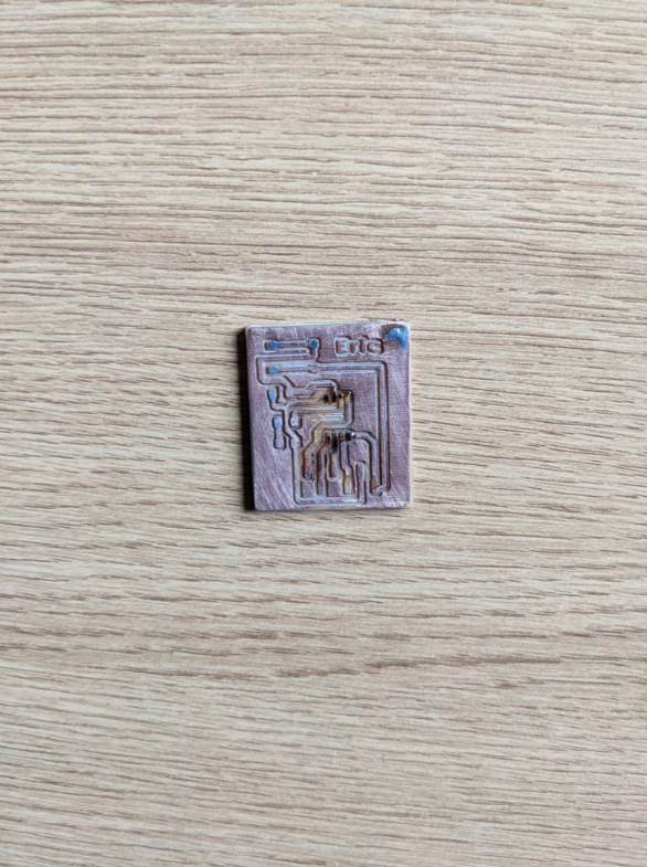
|
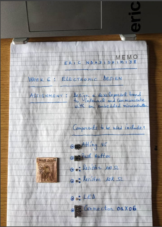
Here below is the generated PCB on the paper while listing all components to be used:
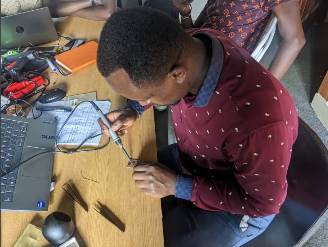
Me while soldering needed components on the board:
Soldering the last component (Push button) on the board:
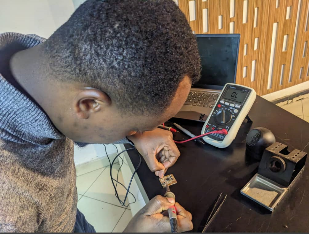
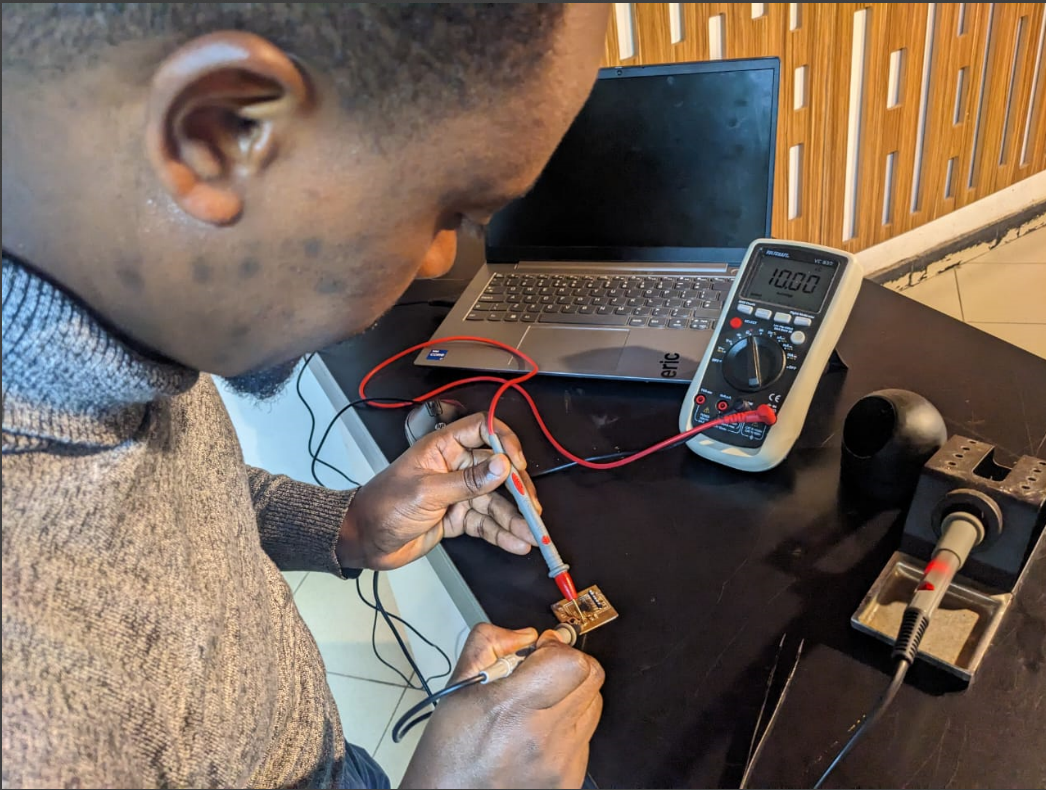
Using multimeter to test board component (Tessing 10K Resistor):
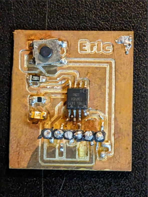
Below here is picture of the PCB with soldered components
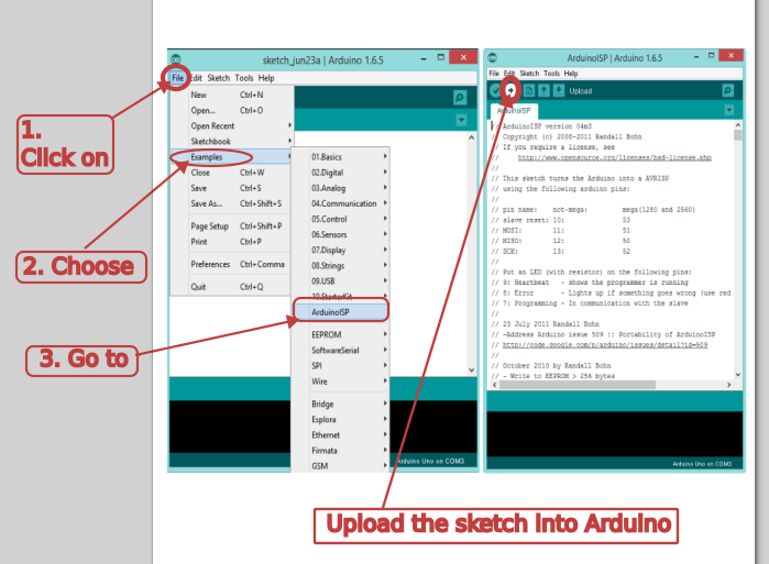
After soldering, the next step is to ensure that it is functioning properly. This involves loading a bootloader before running the initial sketch.
A bootloader is a small program that initializes the main program or firmware of a microcontroller unit (MCU) or other electronic devices. It is typically stored in non-volatile memory, such as flash memory, and is executed when the device is powered on or reset. Its main function is to prepare the MCU for the execution of the main program by initializing necessary hardware resources and loading the main program into the appropriate memory locations.
Connect Arduino to the computer using a USB cable.
               int led=3;

               void setup()
               {
               pinMode(led,OUTPUT);
               }

               void loop()
               {
               digitalWrite(led, HIGH);
               delay(150);
               digitalWrite(led, LOW);
               delay(150);
               }
See the below photo showing blinking LED 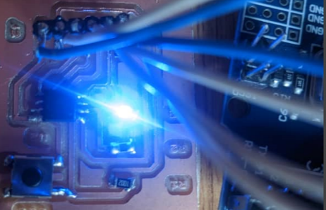
Watch the next video here on right side to see how the ATtiny45 microcontroller successfully blinks the LED