- design idea
- schematic design
- pcb designer design idea: we make pcb from existing idea that is planned before jumping to any step
assignment is about ELECTRONICS PRODUCTION
Group Assignment https://fabacademy.org/2023/labs/rwanda/Group_Assignment/electronic_production.htmlelctronics production is The electronics industry is the economic sector that produces electronic devices.
It emerged in the 20th century and is today one of the largest global industries. about this instruction visit https://en.wikipedia.org/wiki/Electronics_industry
also refer to this LINK HERE
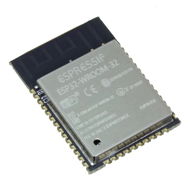
for the assignment mentions i make a pcb board and integrate with embedded microcontroller
so i have used ESP32-WROOM-32 based esp32 microcontroller and CH340 as programmer
to make pcb board there are few steps needed to be followed
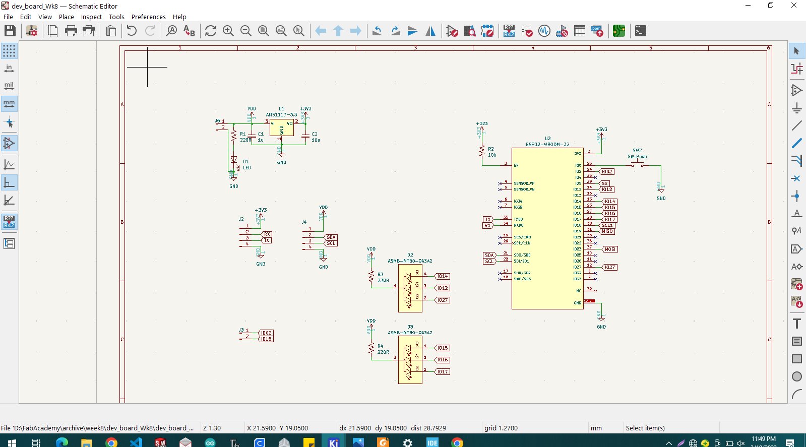
schematic design: this part of design contains componets symbols where we make connections between several components according
to the electrical rule connection and this prepares pcb design
PCB designer: this part brigs us to the final step where we deals with real world, everything we made in schematic
has relations to the pcb any componets symbols in schematic, means that every symbol placed has to be assigned with suitable footprint
at the end we have we make connections between components footprint that are placed on motherboard
so to make pcb designer i have used Kicad software
to implement through these steps there are some requirements, the software used to design schematic and pcb layout design or EDA
EDA is a category of software tools for designing electronic systems such as integrated circuits and printed circuit boards.
The tools work together in a design flow that chip designers use to design and analyze entire semiconductor chips.
Since a modern semiconductor chip can have billions of components, EDA tools are essential for their design;
this article in particular describes EDA specifically with respect to integrated circuits (ICs). refer to this link
for my case i have used Kicad designer and i followed this link https://www.kicad.org/download/ to download the software
then after downloading the software and installed it, it was time to launch the software and start designing which has view layout as it s shown below
what is Kicad
KiCad is an open source software suite for Electronic Design Automation (EDA). The programs handle Schematic Capture,and PCB Layout with Gerber output. The suite runs on Windows, Linux and macOS and is licensed under GNU GPL v3. more about licad visit link https://www.kicad.org/about/kicad/
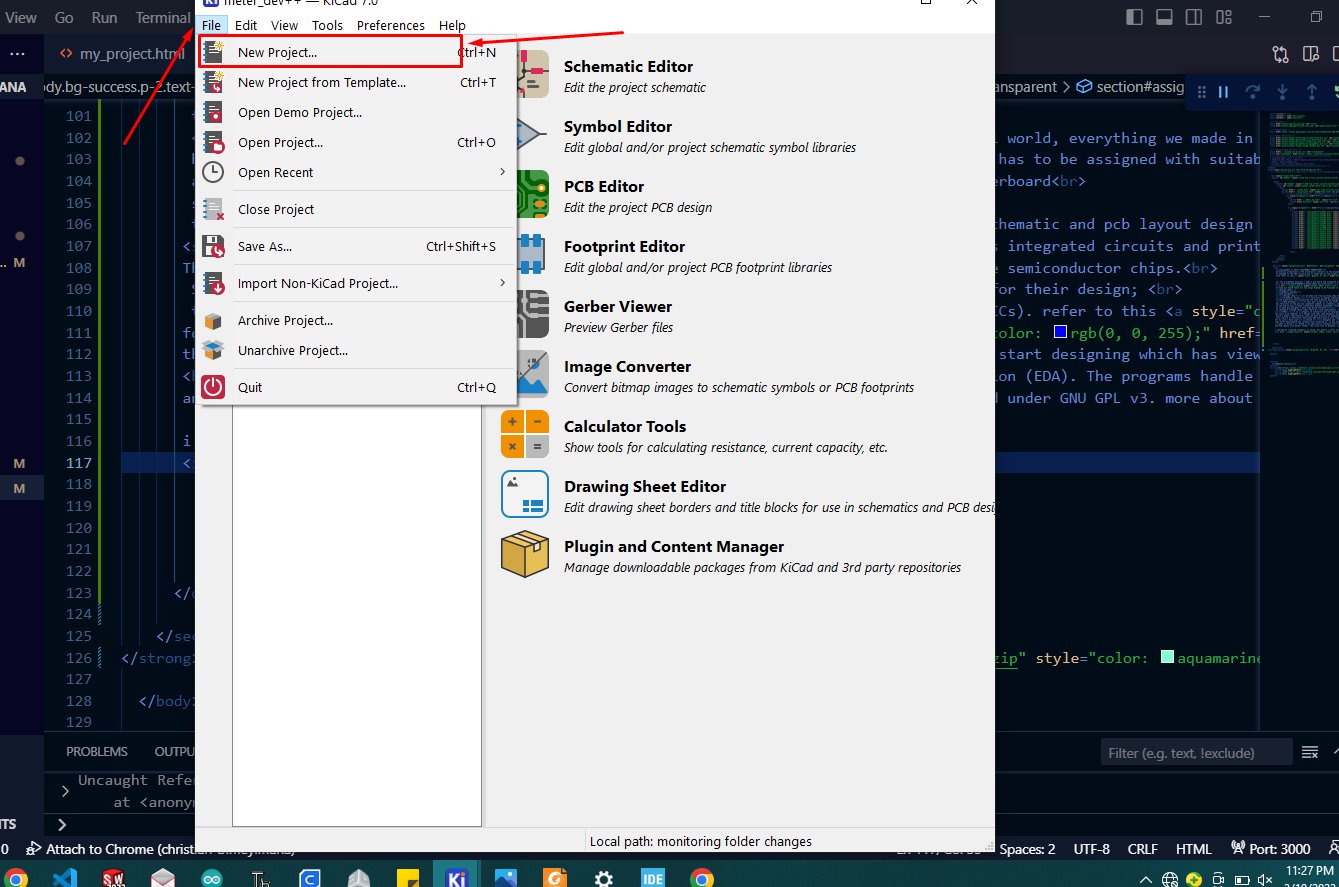
i started by creating schematic in kicad, but before i start with creating new project
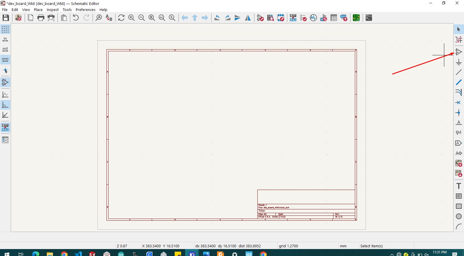
after creating new project that is exactly kicad project format, and that is also kicad user interface schematic editor
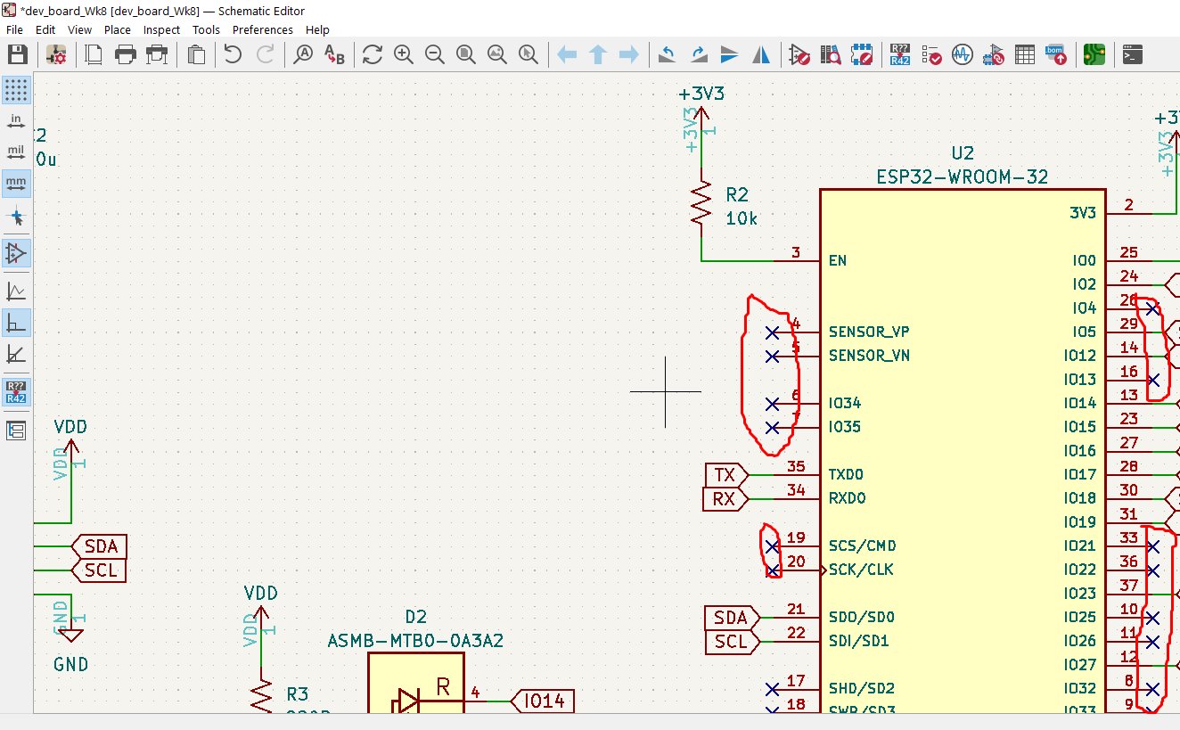
so to click on the shown icon it opens symbol components library, and i searched esp-wromm-32 as i am using it

similar with all other components i place them all and then arranged and make connections where they belong
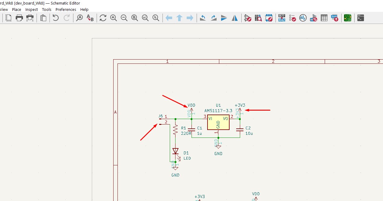
i have made different parts such as voltage regulator with output of 3.3v
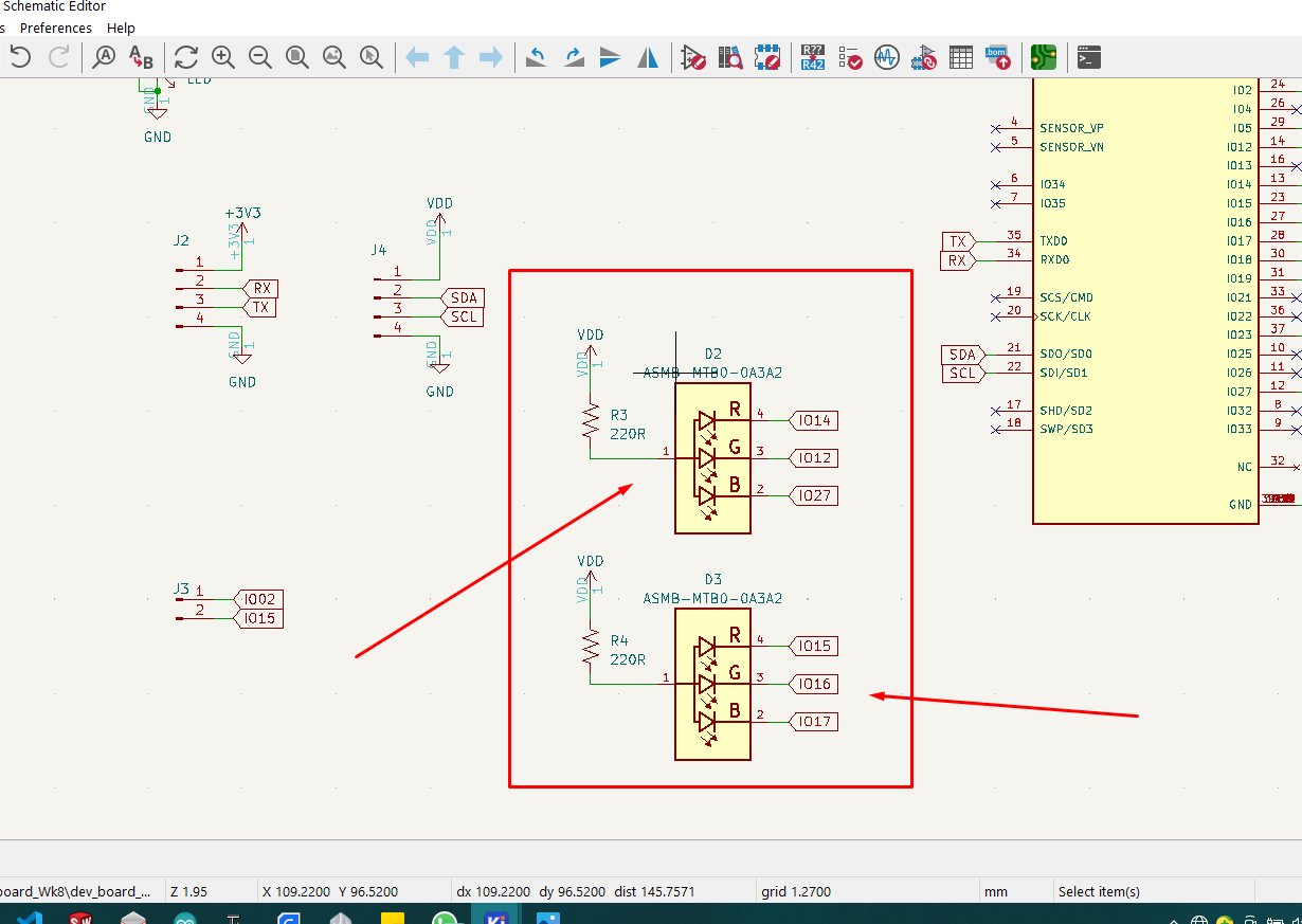
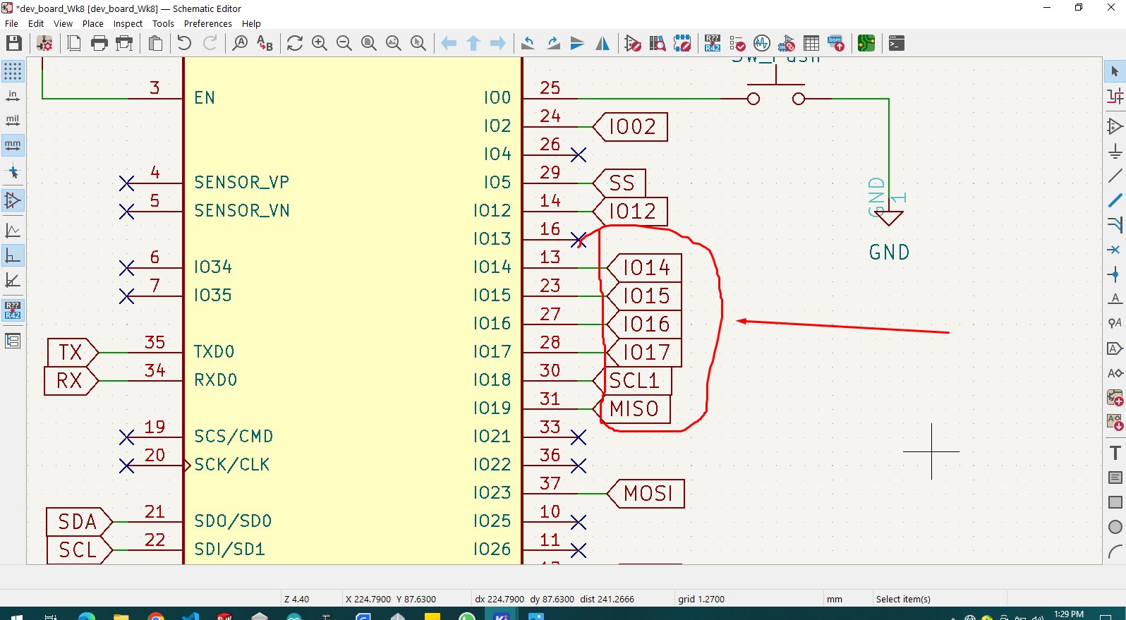
the part of microcotroller where we have ESP32-WROOM-32, connectors and the RGB leds for indication of embedded integration
after making all those connections we the following results
this is the part of the voltage regulator 5v in to 3.3v

and also this the part of leds
connectors

so i searched again for 3.3v and vdd, so these are power flag that connects all pins with it, and hey indicates power rail
followed by lebel, this tools connects two parts without using wires connections where each side has lebel with the same name
so the following is called no connection i have used it on pins which aren't conected on anywhere or unused press Q on keyboard
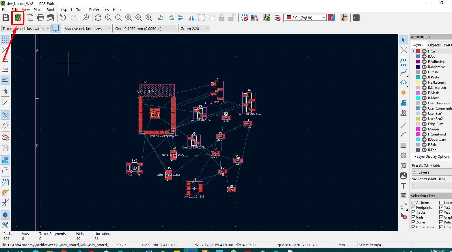
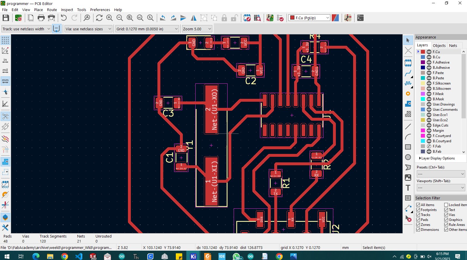
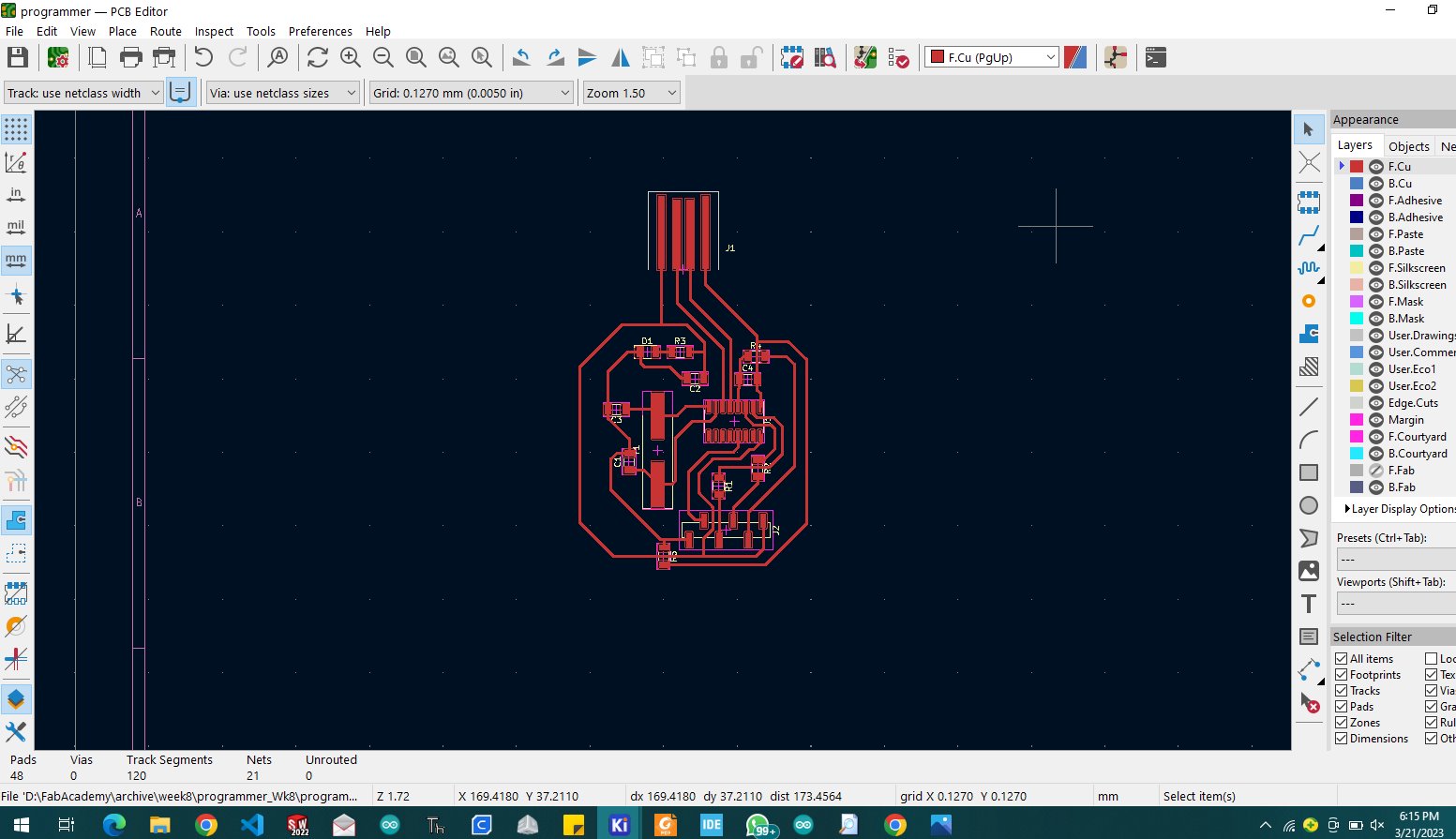
when done with schematic i have clicked on shown icon for pcb editor or navigate to tools>>switch to PCB editor
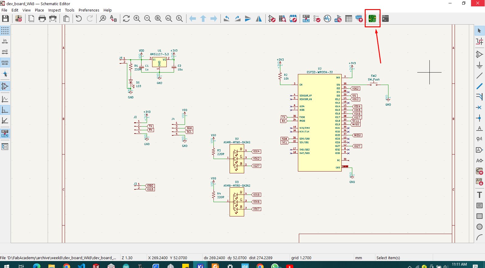
new interface opens where to design pcb, and i clicked on marked icon to integrate schematic with pcb editor
or click from tabs click on tools>>update pcb from schematic

new window opens up and then i click on the button "update pcb"
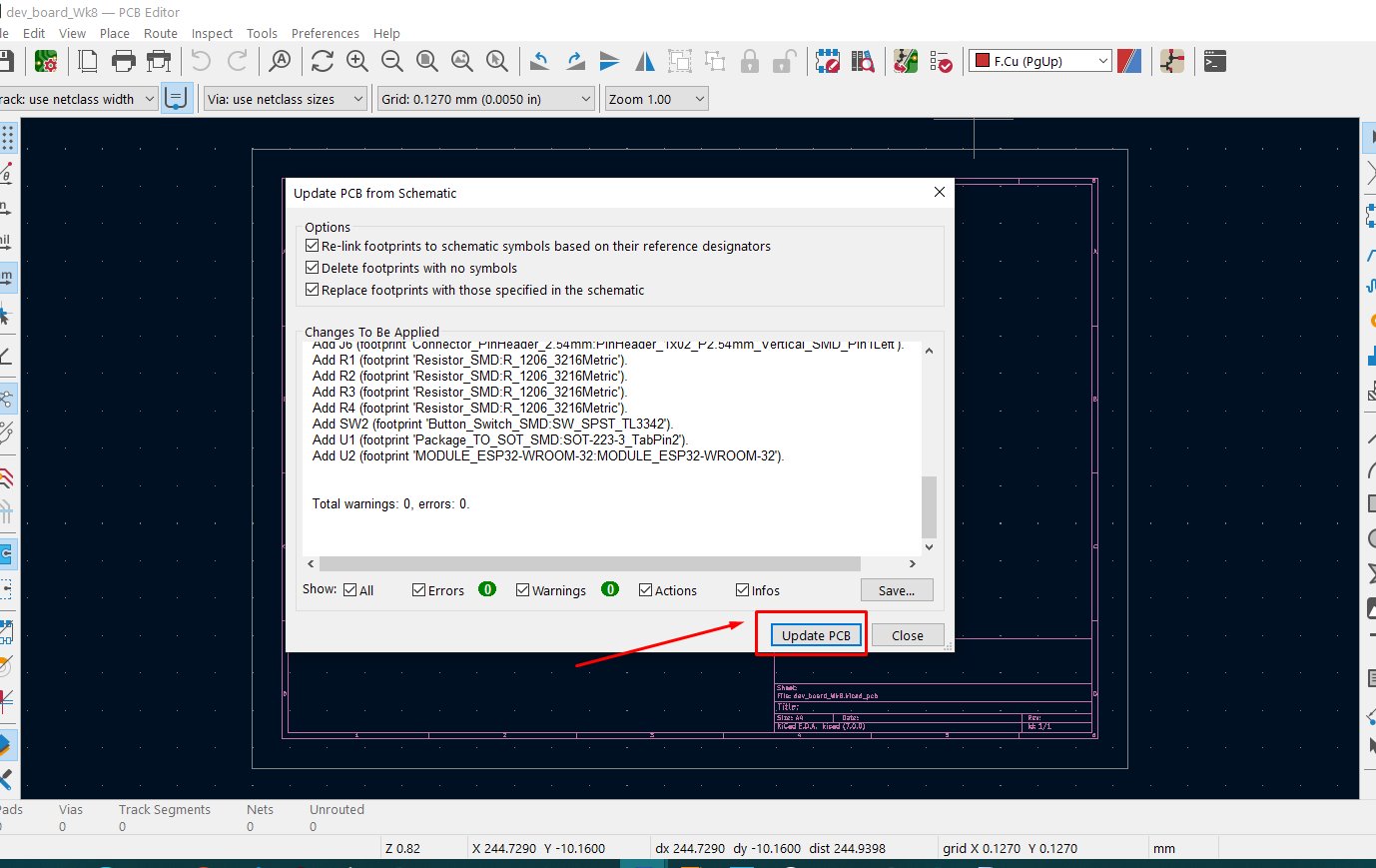
then all components loaded from schematic to be autoplaced to the pcb editor
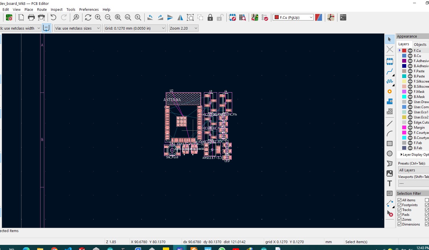
trying to arrange the components accordingly
so after arranging the components together where i can trace then correctly
i clicked on shown icon for tracing and making joints between components
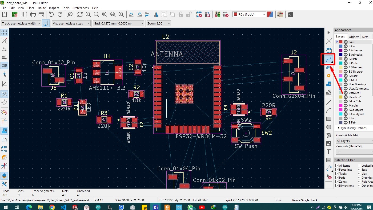
i have joined all componets which are made according to schematic and looks like this
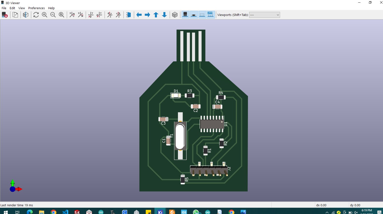
so with the help of shortcut "alt+3" automatically opens 3d model for refering how real pcb looks like

the above pcb i have developed was intended to use it for another and more purposes
where it can be used as development board which can be used to integrate input devices
and the output devices
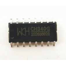
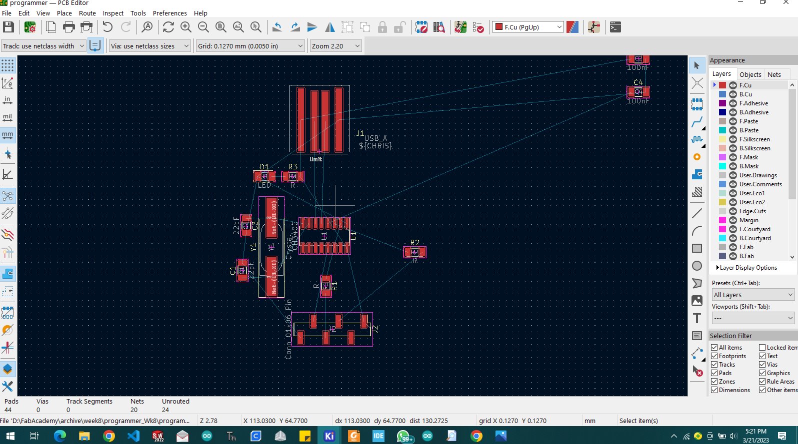
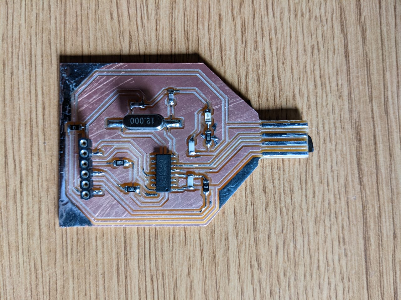
programmer this programmer uses CH340G that convert uart interface to USB interface
the CH340G IC
so this programmer can also helps to flash the above pcb board using esp32
download HERE CH340G datasheet
all footprint associated with symbols loaded
and i started arranging all footprints in a right way to make easy for tracing
i clicked on the marked icon to starting tracing

moving trace from one point to another point

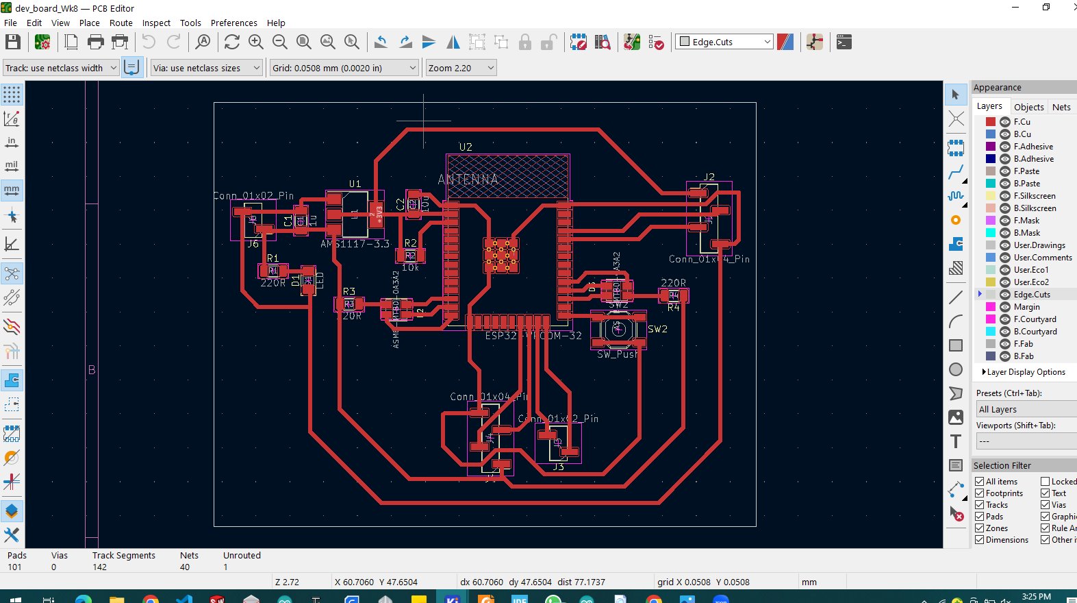
on layers i select the edge cut layer so that i can make the layout of the whole pcb
helps the machine to recognize the layout of the board to cutout

about pcb design rules i have used trace clearence of 3mm the trace width of 5mm enough to drive current
but my trace width i made it bit bigger than needed because my milling machine would cut it out
it is better to make it little bit bigger when you are working with high power tracks
link HERE
for this webpade they explains more in deep about pcb design rules learn more https://www.7pcb.com/blog/pcb-design-rules
from this explains and guide through how to follow with pcb design rules
for my design there's some of the rules has to be modified to start designing depending on my design application and idea
first i click on file from software tabs then choose board setup
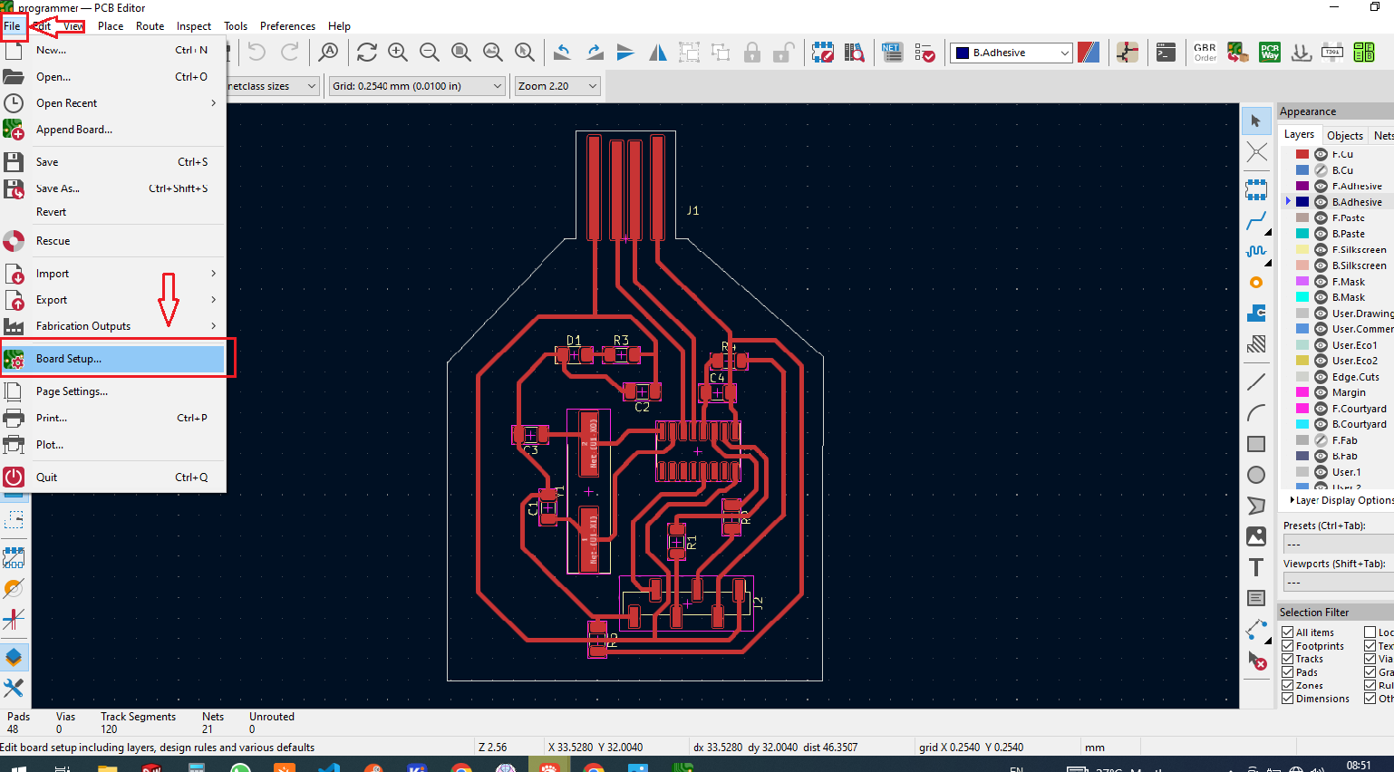
i started with board stackup then to physical stackup in this section i change layers to 2 layers as they are minimum layers and let the others as defaul

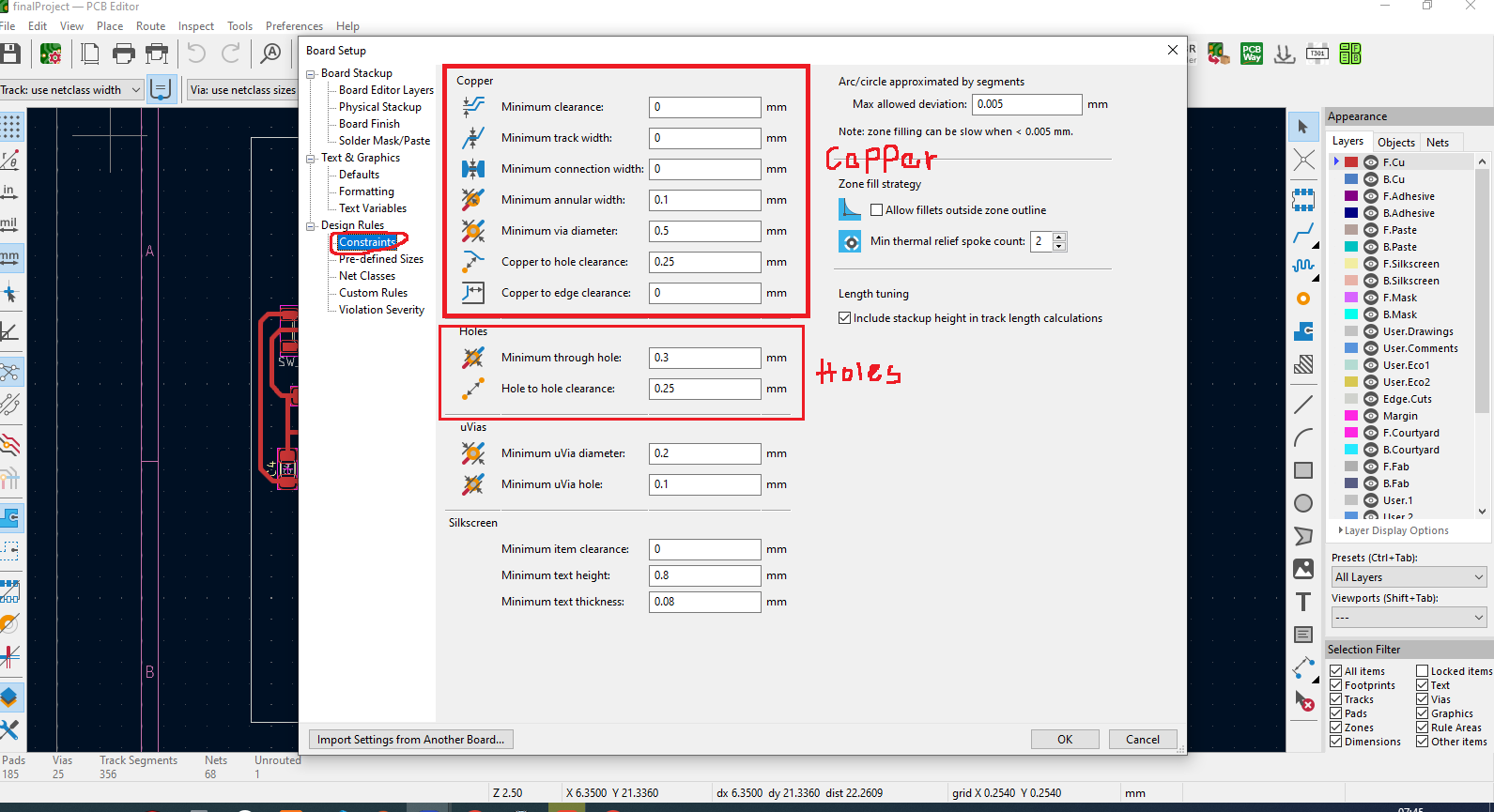
then for the following in design rules >> constrains there are two parts shown in the image copper and holes
in these sections we set the minimum values in design and so all other parameters shown
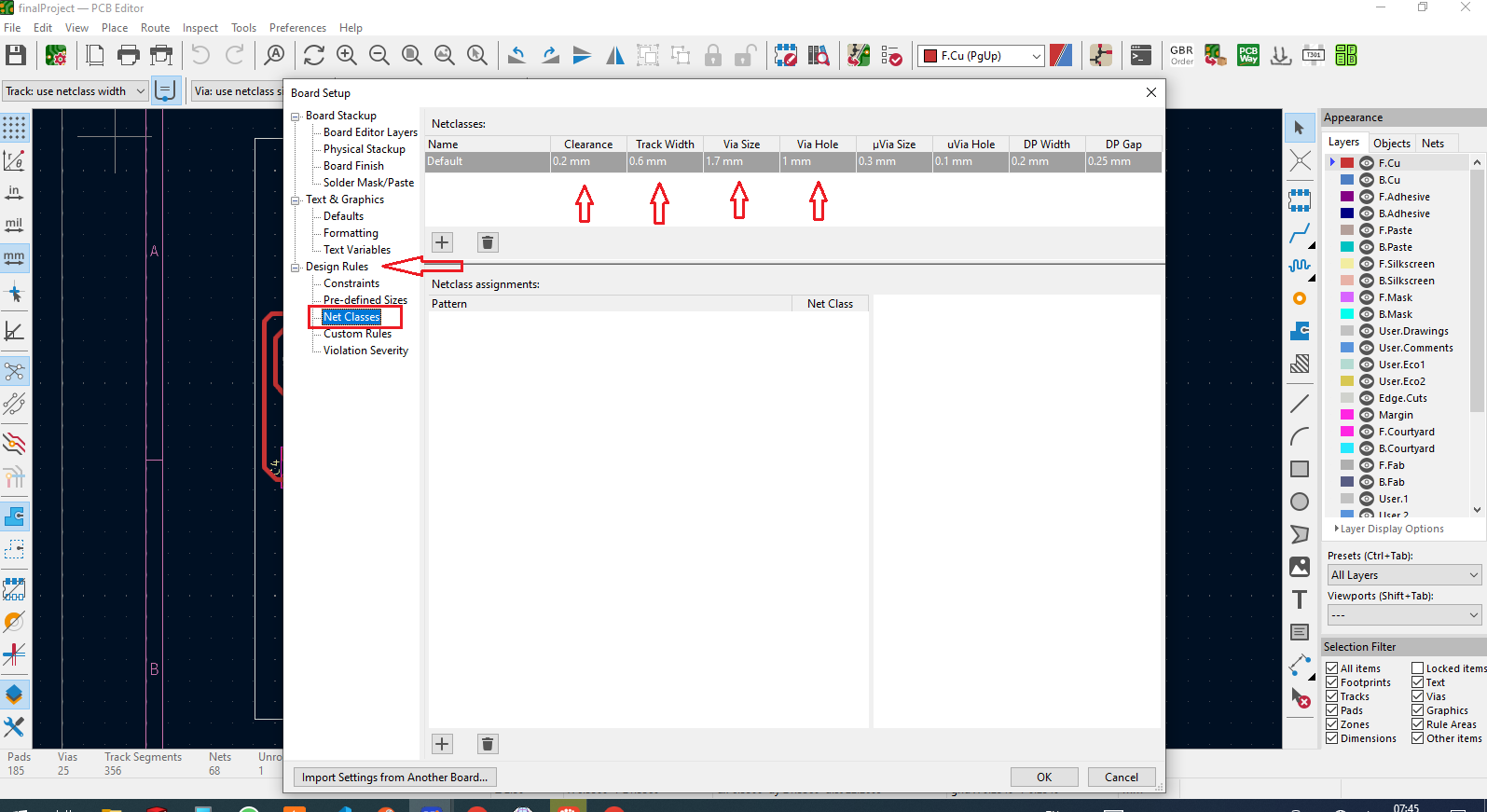
then in design rules >> net classes i set the values of clearance, track width, via size and via hole
depending on board application type we can set the clearence between tracks and pads and set the track width depending on
how much current is driven in pcb track lines,

by opening view>>3d view or shortcut of alt+3 opens 3d model of pcb
then by exporting svg file for generating G-code for milling navigate to file>>export>>SVG

i chose both front copper and edgcuts
and also choose to black and white output
print one page per layer to save them as separated file front copper and edge cuts
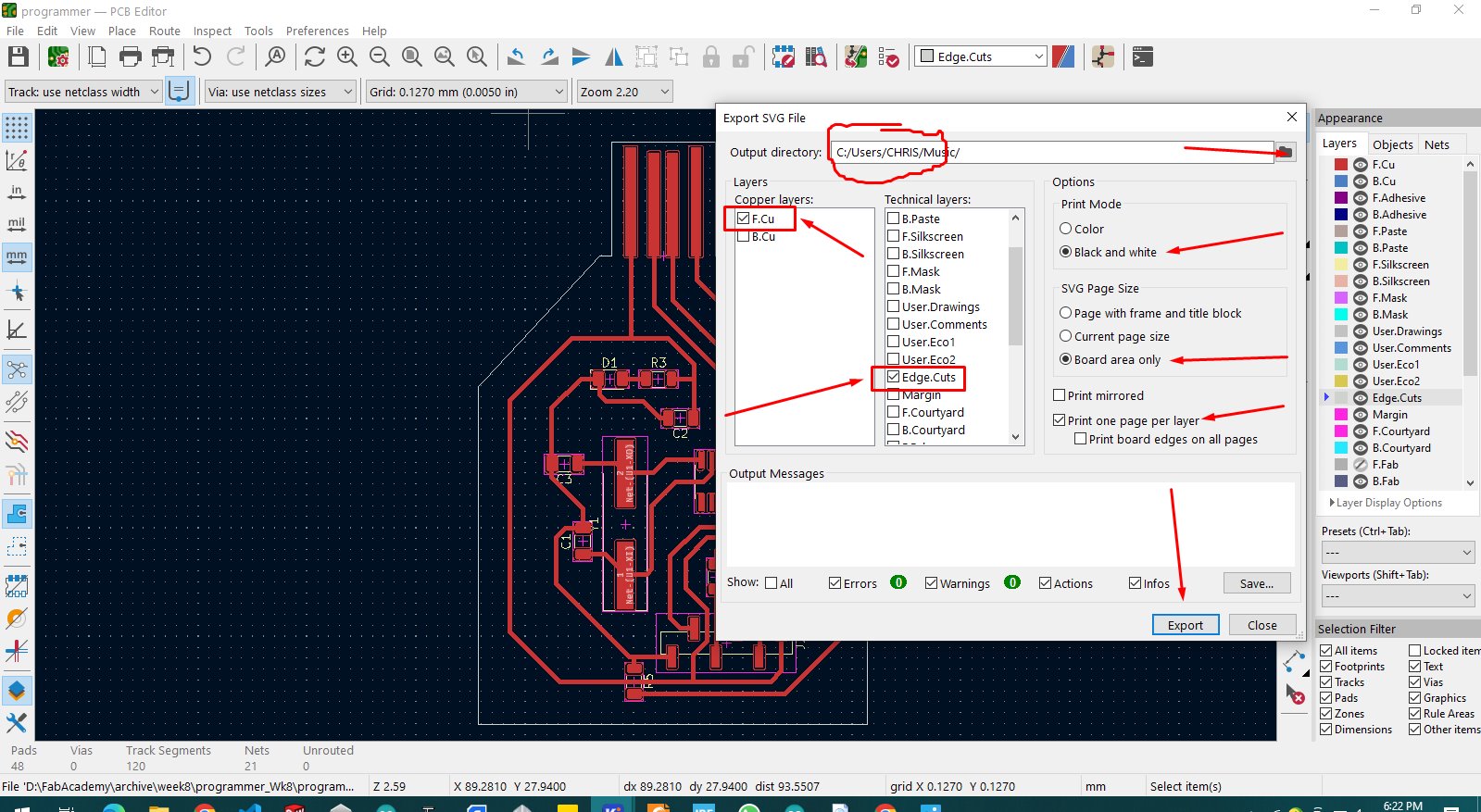
the generated SVG files are imported into mods builder which is used to generate G-code for milling machine visit LINK HERE how i generate G-code for milling
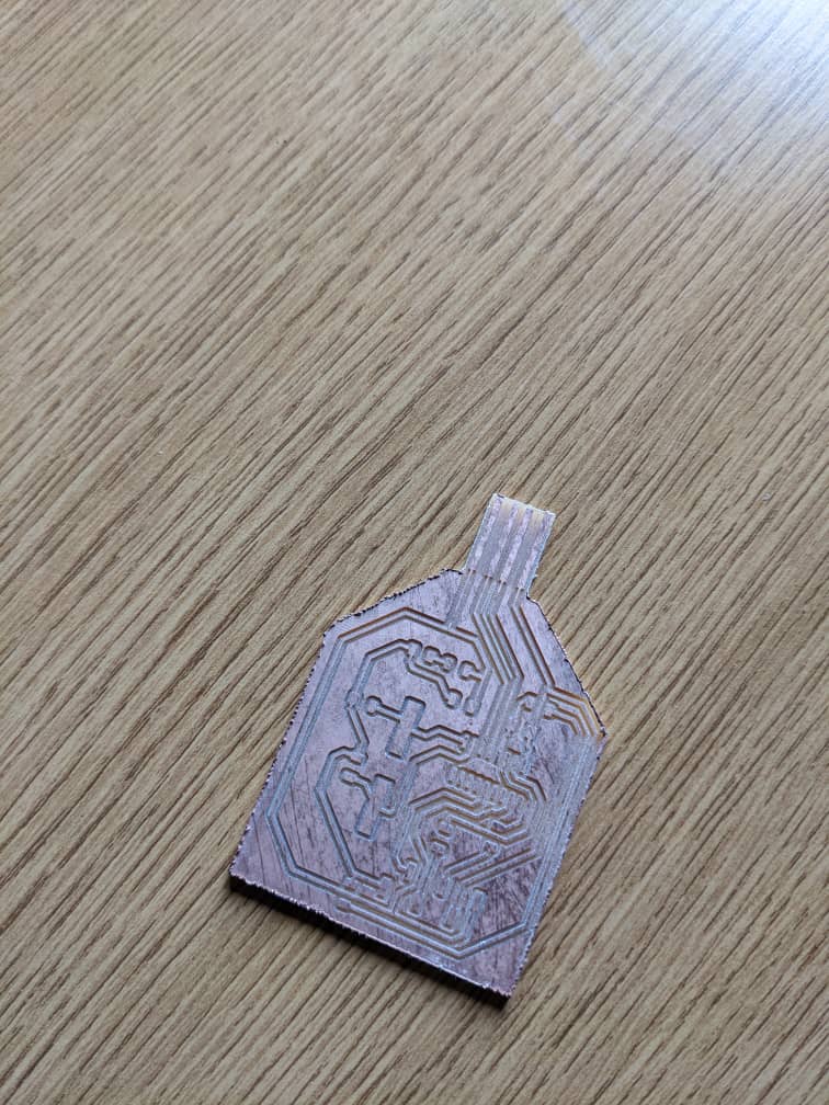
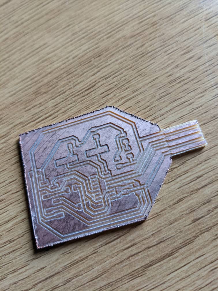
then the pcb was made successfully

i gently broke it out from the bed and then it was ready for adding components and soldering
started soldering all components on pcb so the clearance between copper traces was a bit small so i had to be more
more carefull to avoid making shortcircuits

few moments later after placing all componets and soldering i have plugged device into my computer
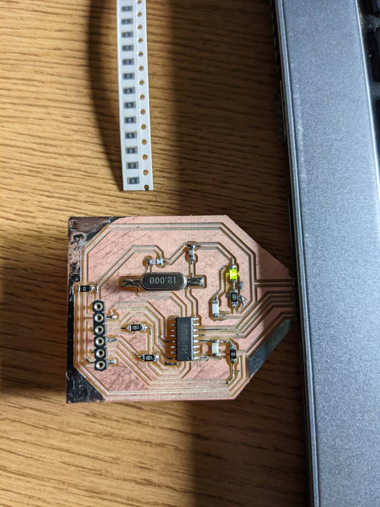
when done with soldering i plugged the device in my computer to check if it successfully done
and when i plugged in it sounded as detected but it was not recognised
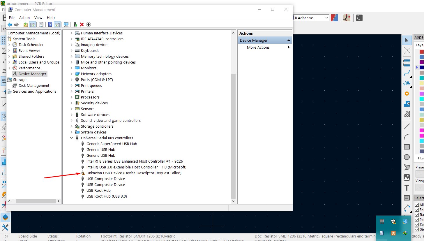
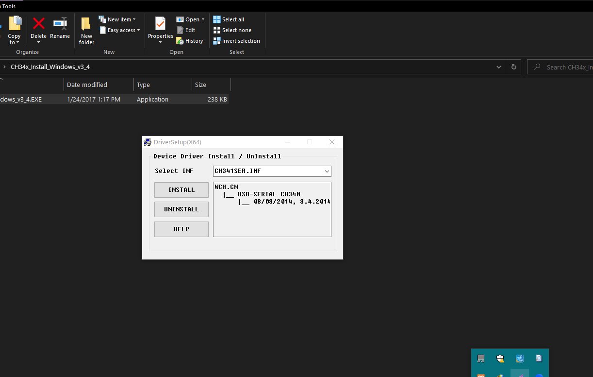
to make this device recognized by computer there's driver for CH340G which to be installed first
if not the device will not be recognized by computer so download it from here
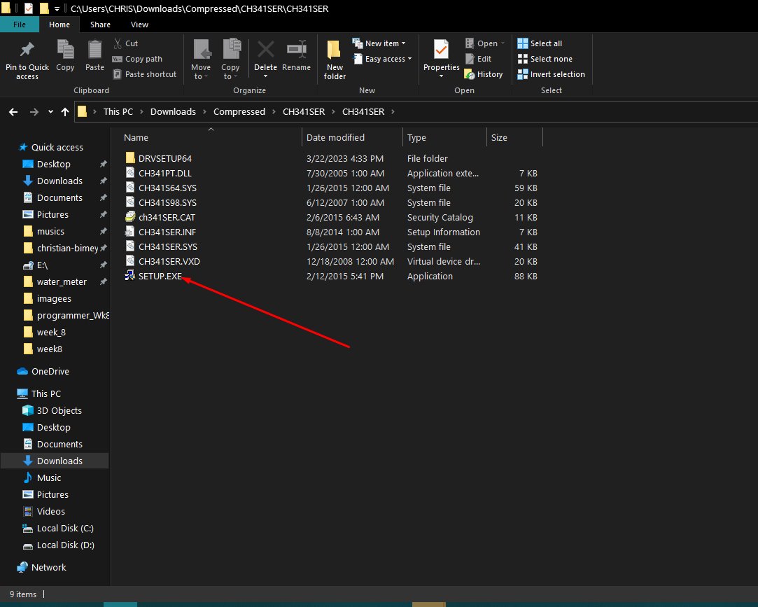
and click install to open it
after installing driver i thaought it done and good to go but i had an issue because computer didn't recognise again
i troubleshooted the device i changed the ic but the problem was not fixed at all
and i realised that the problem wasn't device but computer i tried to unistall drivers and reinstall it again
not fixed again so i tried to find solution to solve this issue
i came with this solution to troubleshoot the drivers to go trough this simply press window key + R
and type in following command
msdt.exe -id DeviceDiagnosticenter
the same window will popup and click next for starting diagnostic
i followed all steps i am requierred to follow so computer also required me to restart the system

after showing up in device manager it was successfully working
the programmer i have made will be used to program esp 32 that will be used in following work assignments