- project idea
- making schematic
- making pcb layout to implement through these steps there are some requirements, the software used to design schematic and pcb layout design or EDA
- schematic editor it is a section where we make circuit diagram you can get there a different components
- PCB editor this section is needed when we are done with making schematic diagram
- symbol editor we use this section when you can not find a desired components and try to make your own component from scratch
- footprint editor this section also offers designing area where we can not find component footprint
- gerber viewer when we are done with designing PCB, we generate gerber files that contains pcb footprint position and all about pbc file design
- image converter this converts normal image format to kicad suitable files and readable like when we place logo on pcb
- calculator tools this tool helps to calculate pcb properties such as current and traces
- drawing sheet editor
elctronic design
group assignment testing equipments https://fabacademy.org/2023/labs/rwanda/Group_Assignment/molding_casting.html group pageelectronics design is a process of making electronic project from idea to sschematic then to pcb hardware
to implement all these process we use specific software aimed to design about eectronics
there are few steps needed to be followed for elctronic design
EDA is a category of software tools for designing electronic systems such as integrated circuits and printed circuit boards.
The tools work together in a design flow that chip designers use to design and analyze entire semiconductor chips.
Since a modern semiconductor chip can have billions of components, EDA tools are essential for their design;
this article in particular describes EDA specifically with respect to integrated circuits (ICs). refer to this link
for my case i have used Kicad designer and i followed this link https://www.kicad.org/download/ to download the software
then after downloading the software and installed it, it was time to launch the software and start designing which has view layout as it s shown below
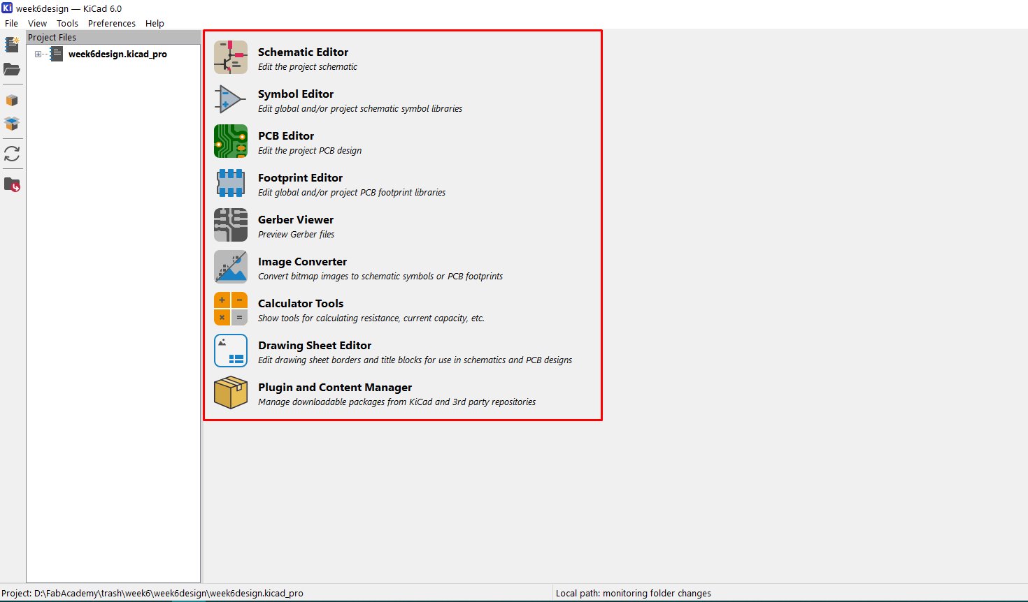
what is Kicad
KiCad is an open source software suite for Electronic Design Automation (EDA). The programs handle Schematic Capture,and PCB Layout with Gerber output. The suite runs on Windows, Linux and macOS and is licensed under GNU GPL v3. more about licad visit link https://www.kicad.org/about/kicad/
it has different tools such as
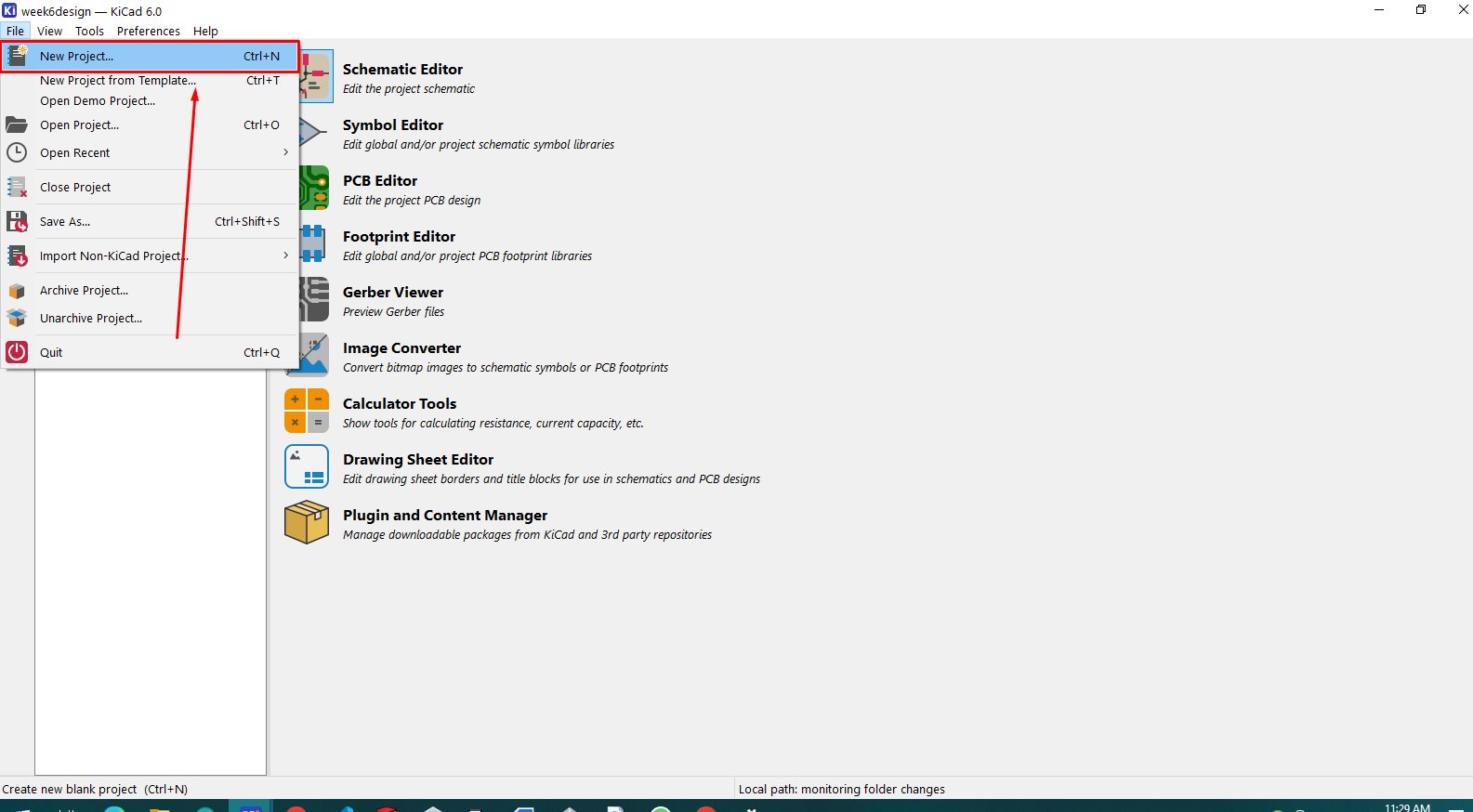
then to start the design click on file>>new projec and new window opens with directory location will openup and the save with desired name
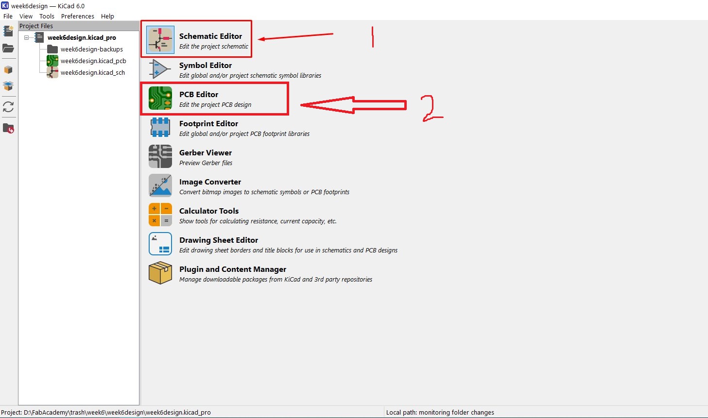
after saving as new project and then click on schematic editor which opens new loyout for starting circuit diagram
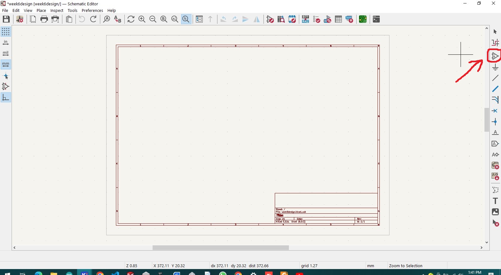
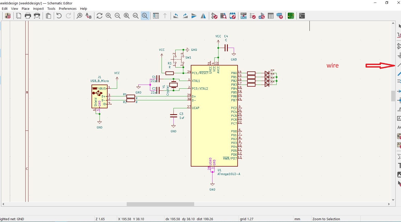
when a new layout opens up then click on the symbol shown in the image, to start placing first components in editor
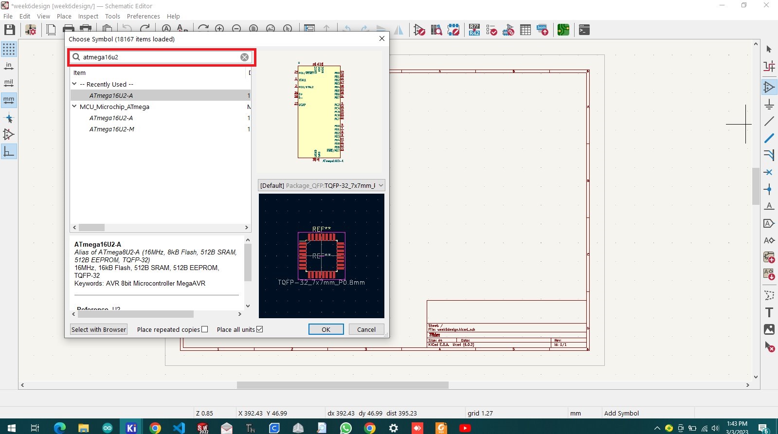
new components window will popup directly then there's searchbox where to find any components for my case i was looking for "atmega16u2, capacitors, resistors, LEDs, crystals, and usb"
then after selecting components that i need i started arranging them in accordingly way, by using wire tool shown in the image to connect pins using wire line
steps followed to make successfull design
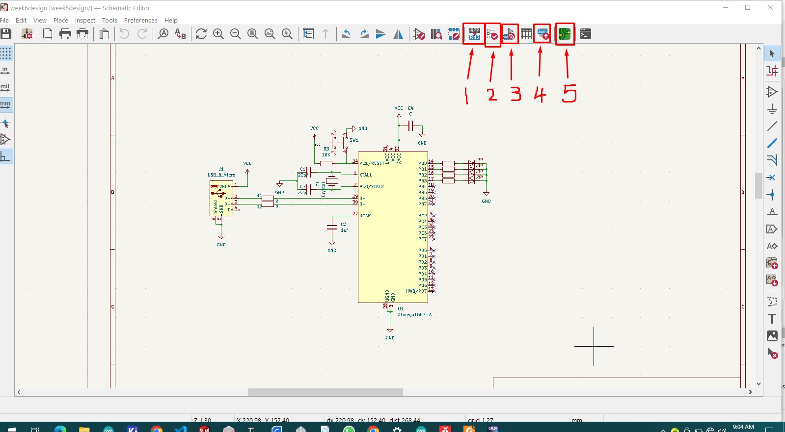
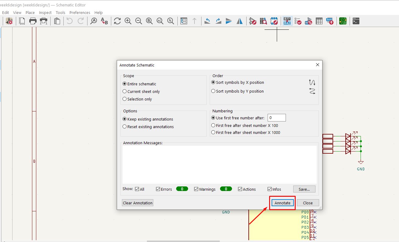
the following step is to annotate the commponents, annotation is a way of renaming components resignators for example resistor has symbol of "R" we annotate as "R1,R2,R3...."
annotation is labeled as 1 shown in the image above
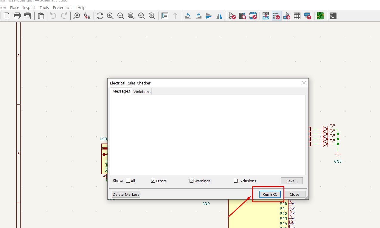
lebel 2 is second step after annotation, this is called ERC test this tool test if there's some errors made during schematic design or electrical rule check
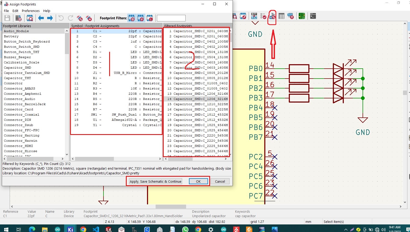
then next step is to assign components symbol with footprint accordingly, just to click to the icon shown
then the new window will popup with all selected components and the library of footprint
and then we assign symbols and footprints depending on what we need to assign
the section lebeled as 1 is the part of our components list the other named 2 is footprint section when finnished assigning the click apply and ok
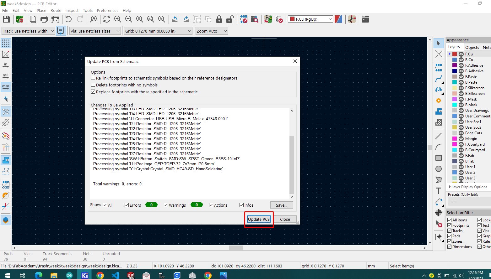
by clicking to PCB icon we shift to pcb editor to the icon named as 2 and then we also click to shown icon to synchronise pcb with schematic
the opened window requires to click on update pcb and load from schematic to pcb by its footprints
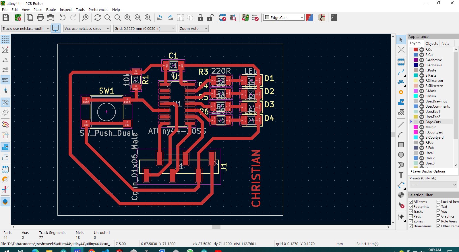
after updating the pcb all components with assigned footprint will automatically placed in pcb layout design
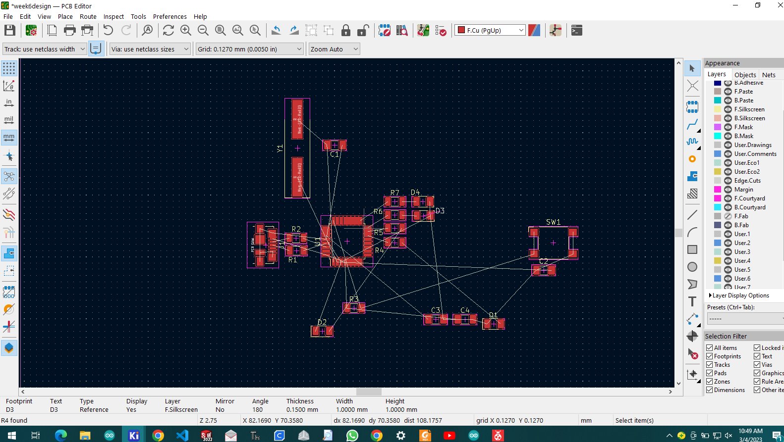
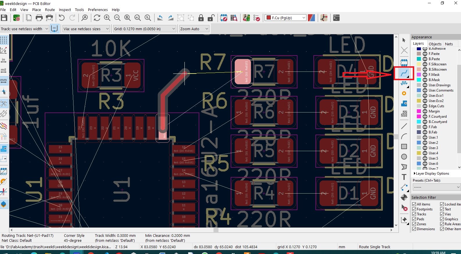
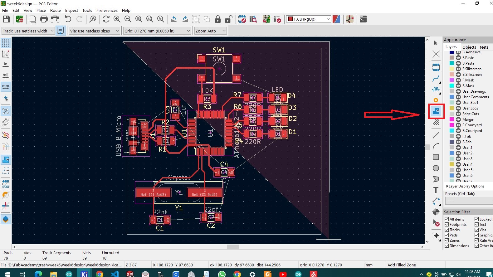
after the arrangement of the components we pick routing tool for connecting components and we join them all according to the schematic
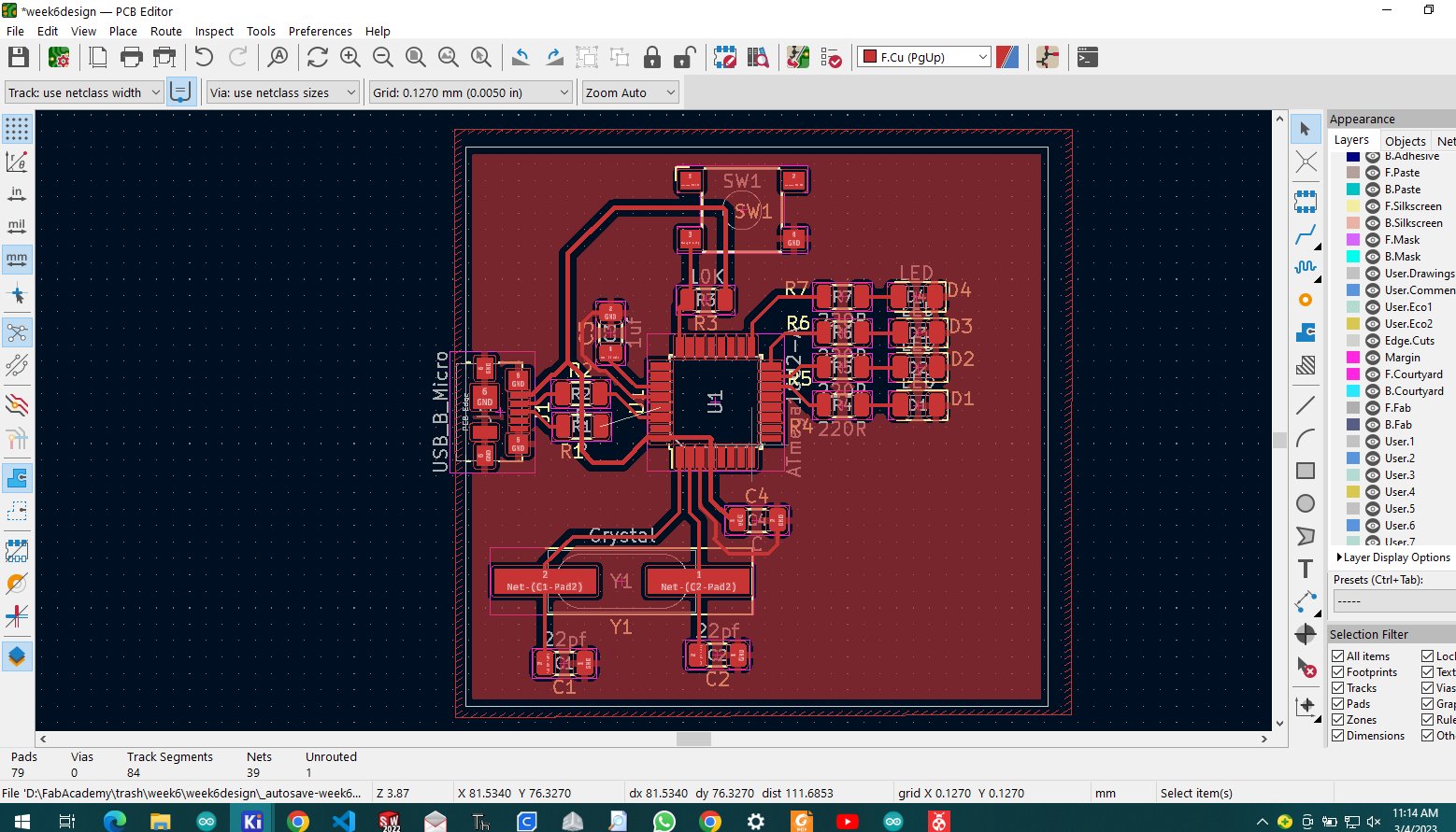
then we make the ground plane to connect all ground pads together
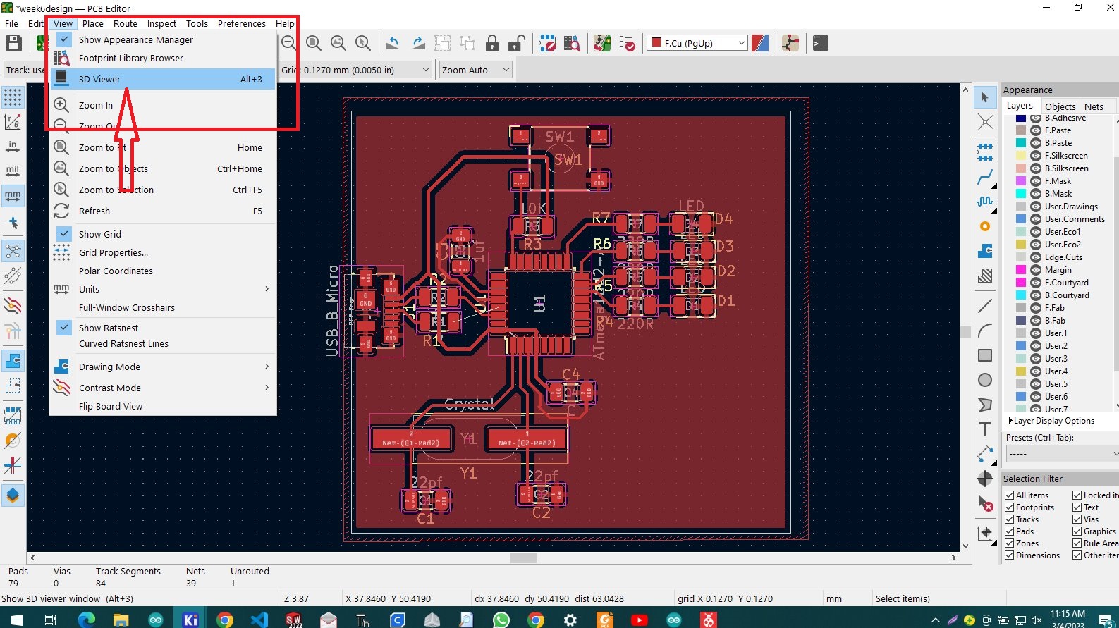
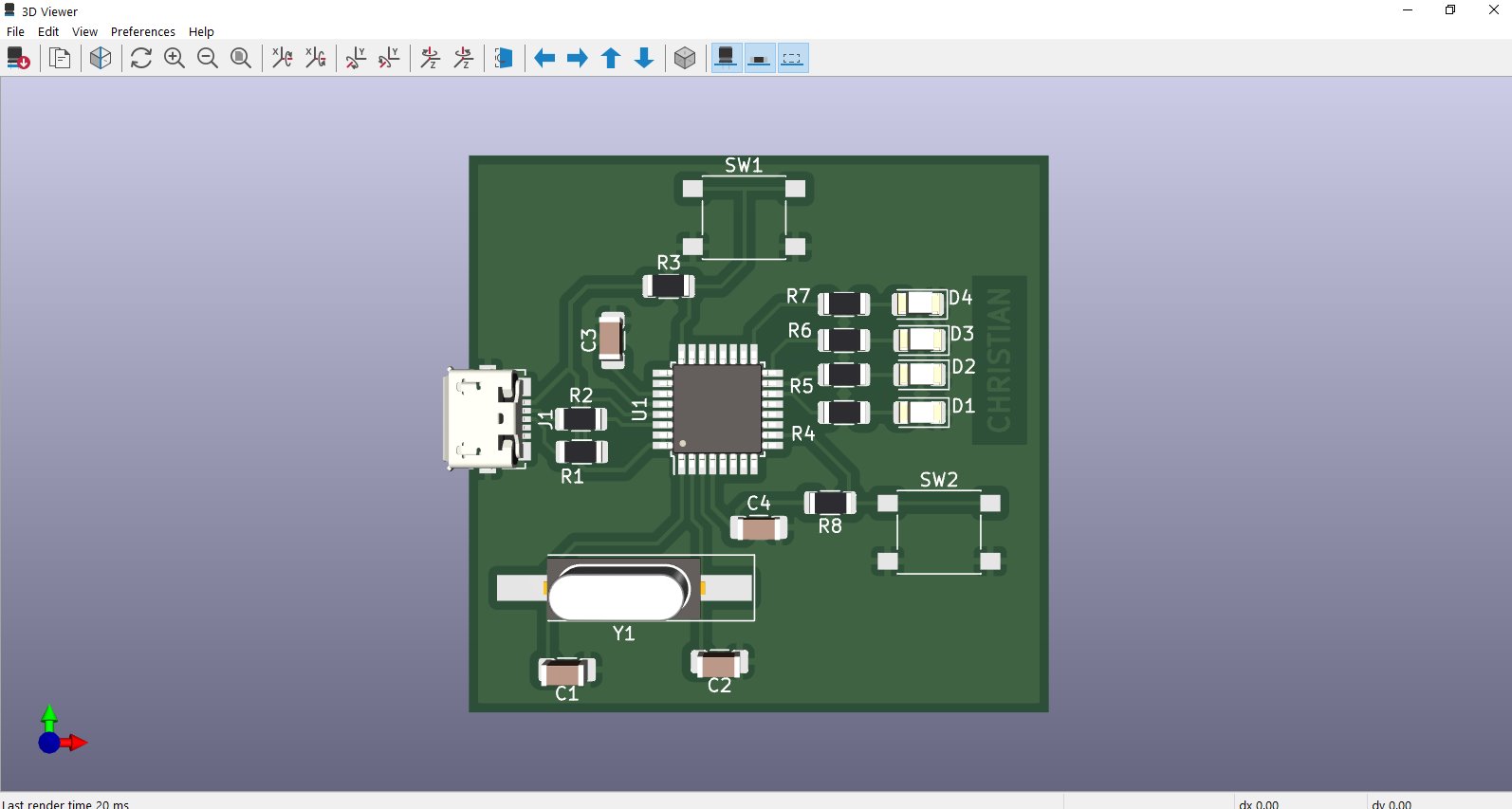
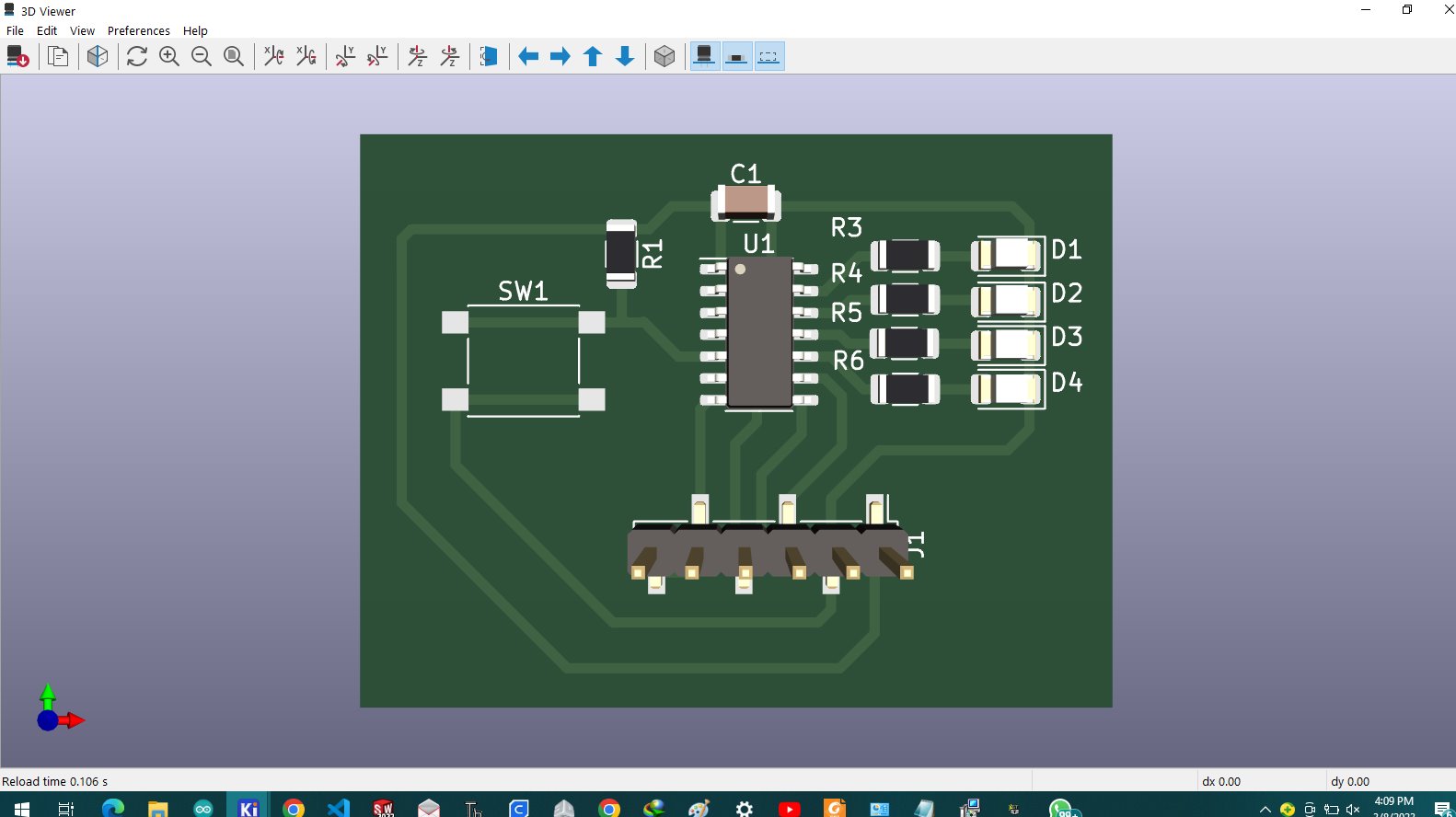
when done simply navigate to tabs>>view>>3dviewer. or alt+3 shortcut
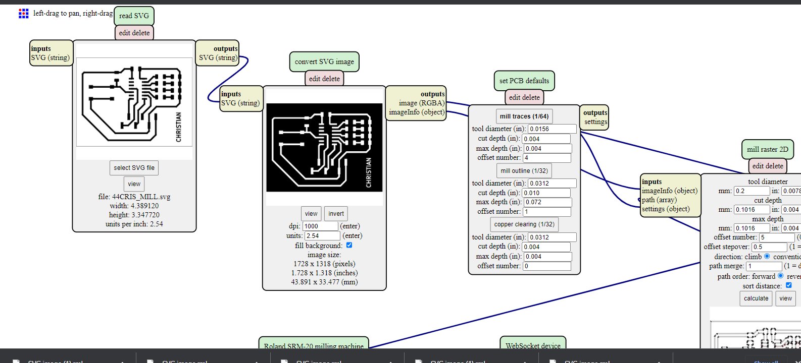
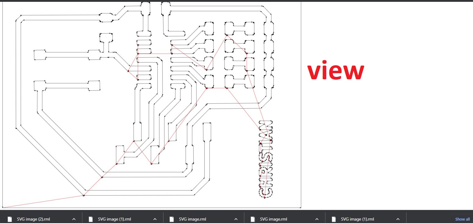
after all done we export as SVG which is supported with KiCad
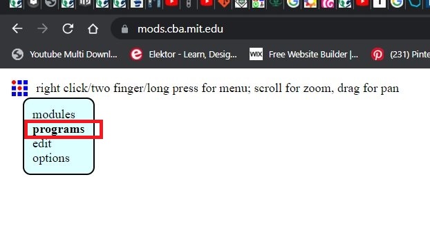
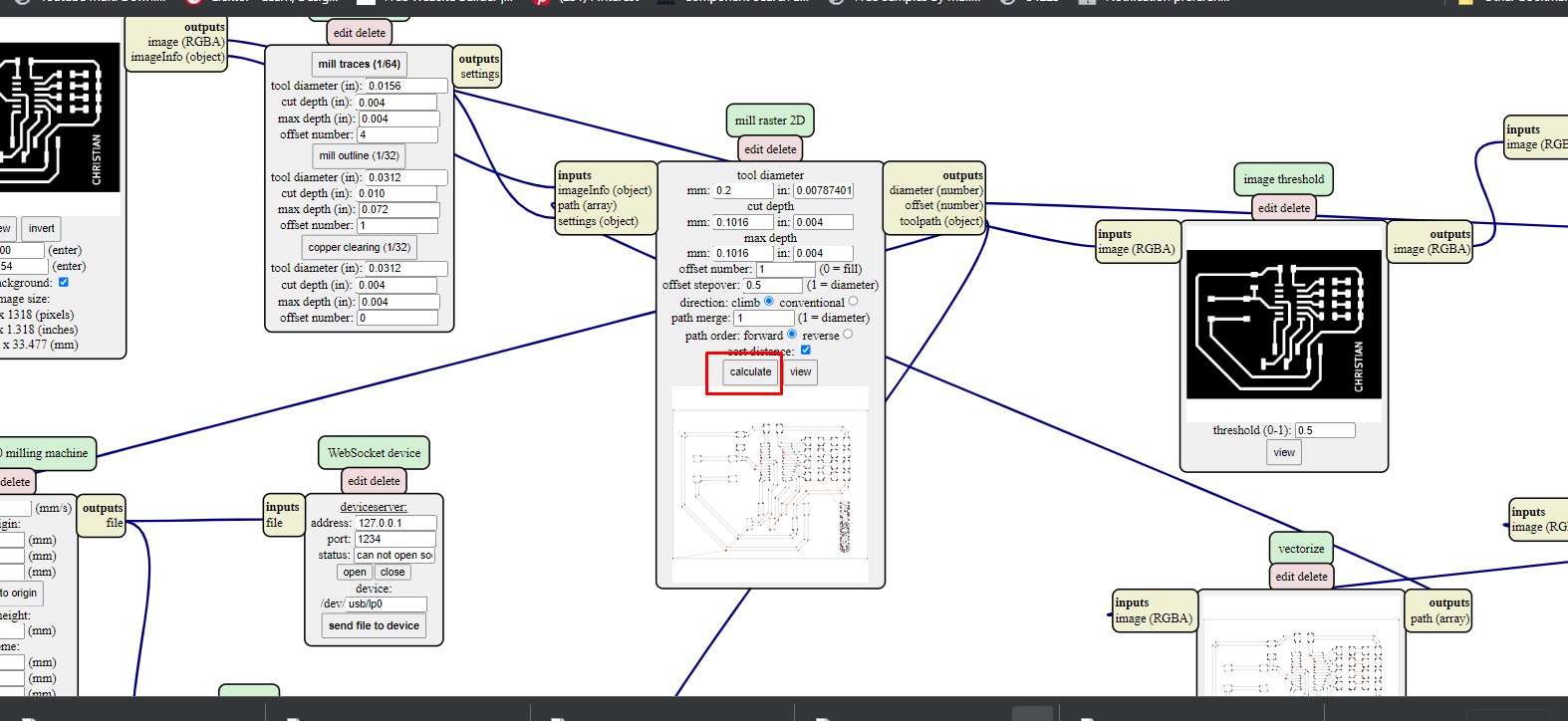
process to export G-code for milling the pcb we open the link following to configure some parameters https://mods.cba.mit.edu/ in few steps to generate G-code
in opened page right click on the icon and choose programs>>open server program
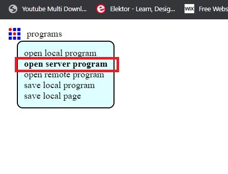
the we choose the milling machine and format for my case we have SRM-20 and because we have used Kicad and it support only SVG export
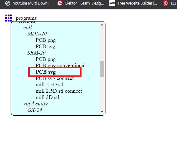
then we import the SVG file we generated from kicad
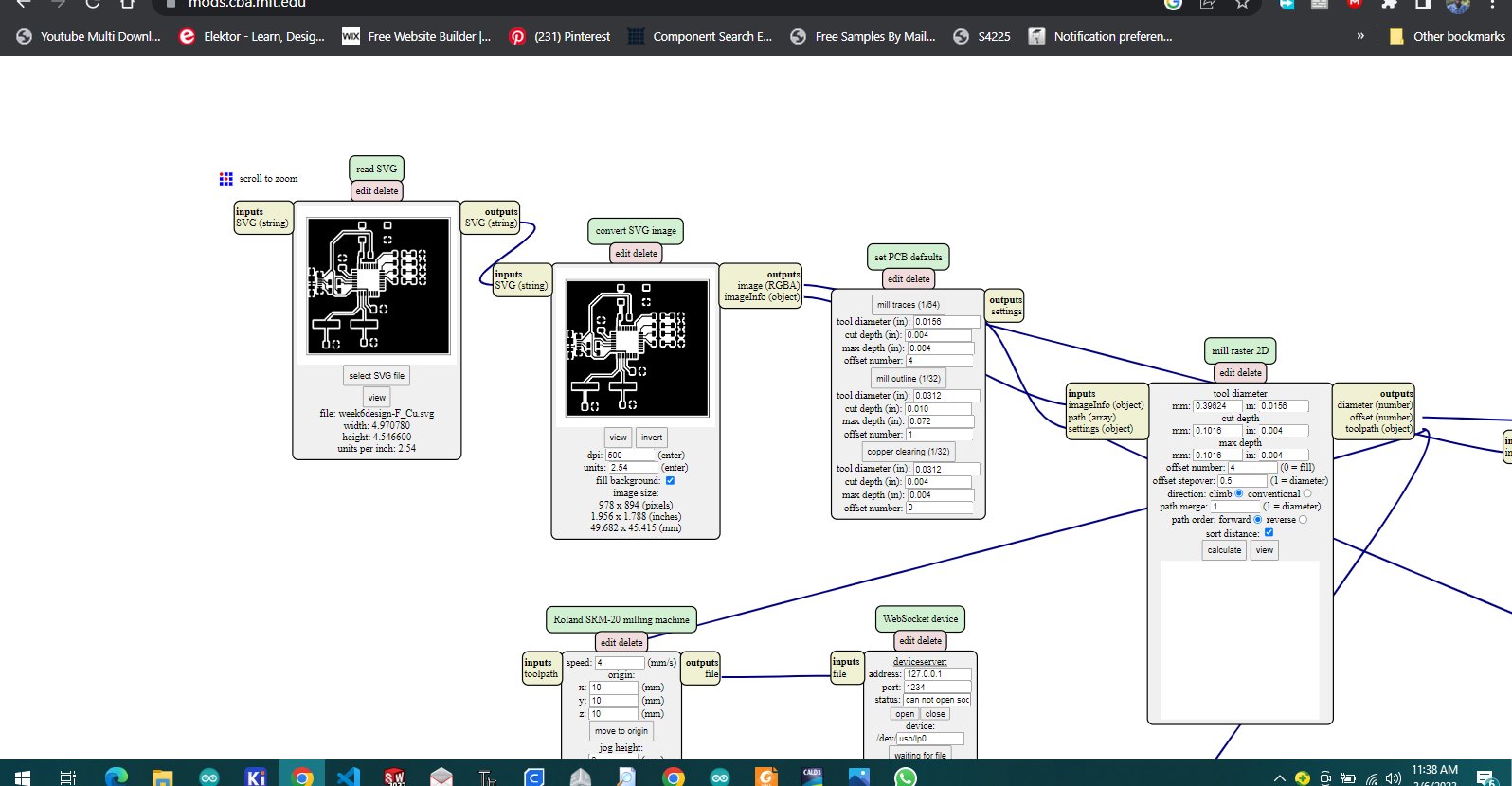
we choose mill tracebutton when we are engraving the pcb traces but when we need to cut the pcb layout we choose mill outline
selecting pcb layout cutting
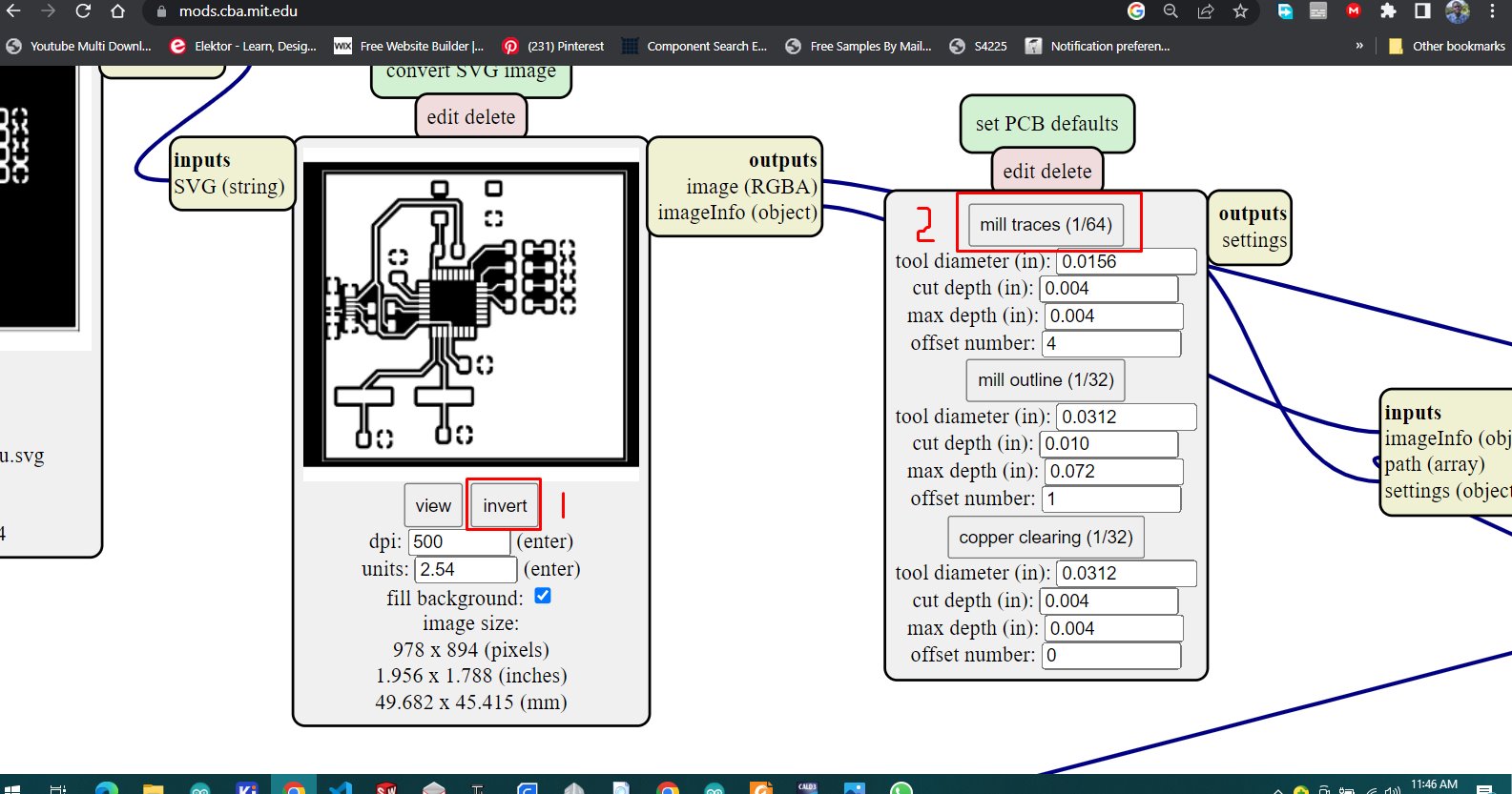
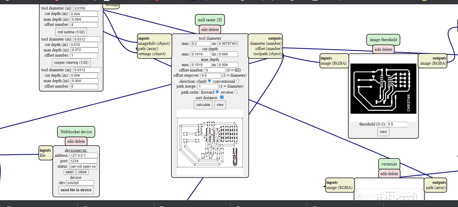
if the file shows up in the we change dpi to 1000 to manage the resolution of the milling and invert to make machine
set the tool diameter in mm or in distance our tool diameter is 0.2mm
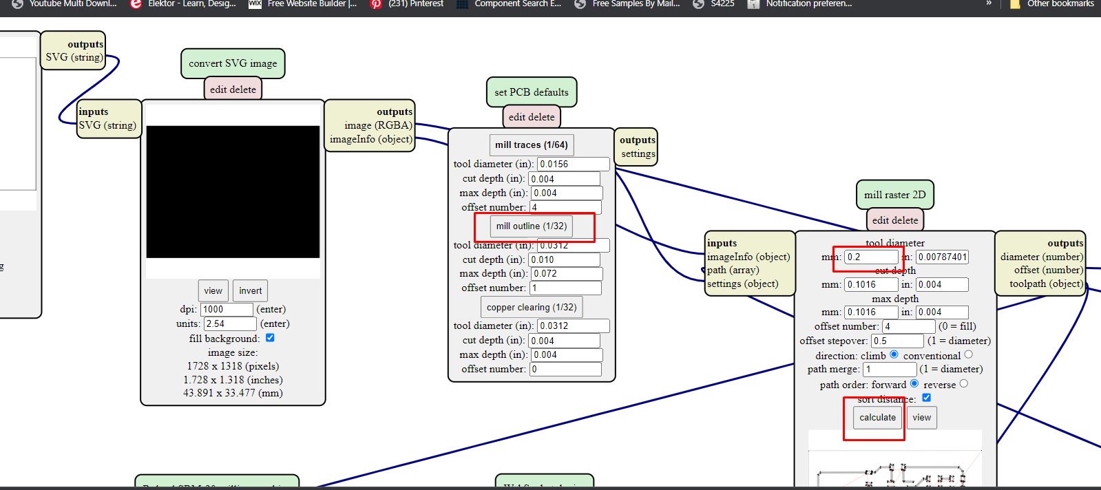
before clicking calculate we set the orgin of machine from 10xyz to 0xyz
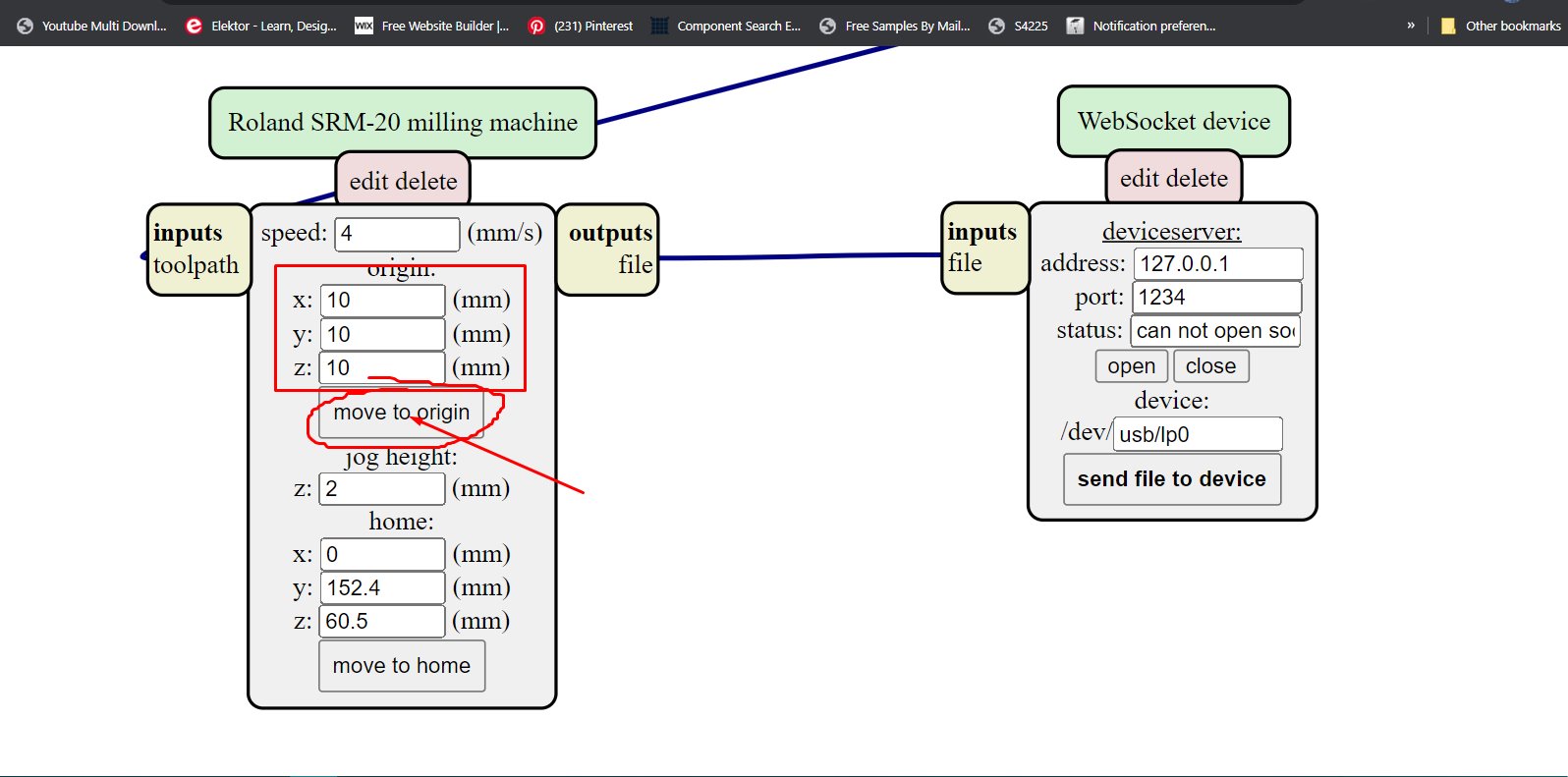
we make block that manages saving G-code file
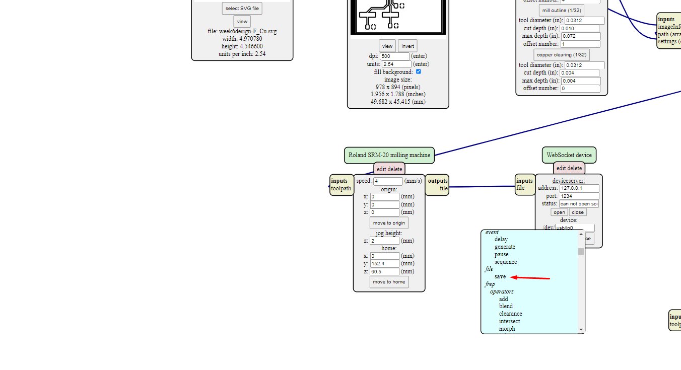
and we connect output file to input file
then from all steps mentioned above i have been occured with issues that microcontroller atmega16u2 i have used above was out of stock we have found in local store so due to time which was not enought i have tried different microcontroller then
with all process i have used while making above schematic and pcb is slightly the same as the following pcb with different microcontroller
download here ATTINY44 datasheet
i shifted to ATTINY44 and changed schematic with pcb then
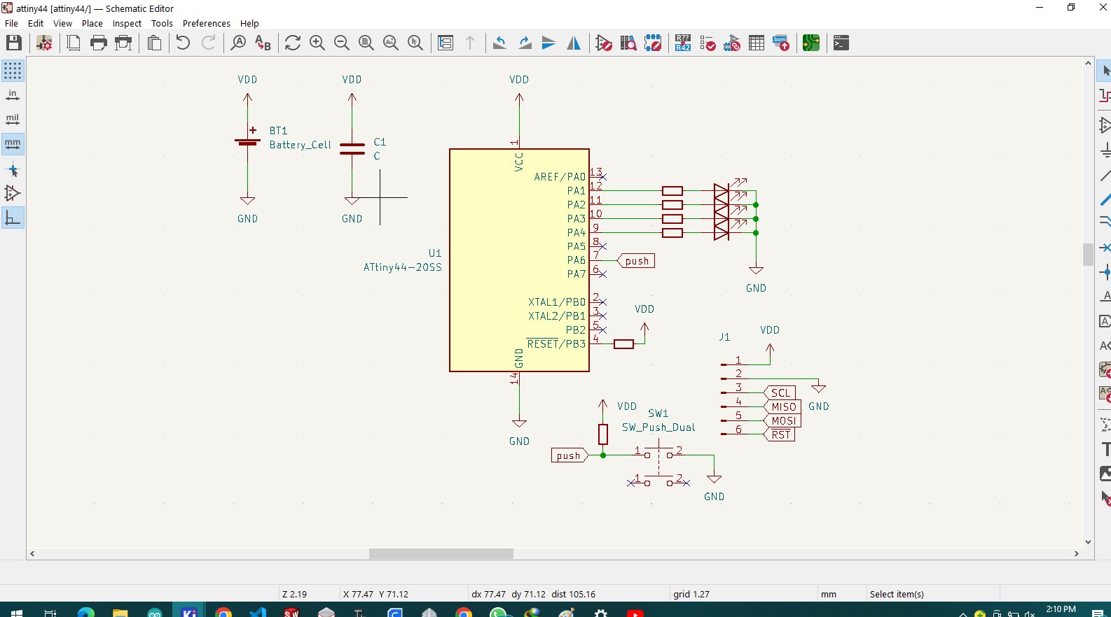
after making this schematic then shift to to pcb editor and design pcb depending on schematic made
by making this pcb i followed all these steps mentioned above to design from schematic to pcb
the when done with pcb editor i checked to 3d model view to see how it looks like in real
to make G-code for milling machine i stepped to https://mods.cba.mit.edu/
in our lab we have roland milling machine to set up the machine we use v carve software
we launch the software and first thing to do is to set the orgin of our bed in XY and Z axis of the bed
the pcb came out finnished after sometimes of milling
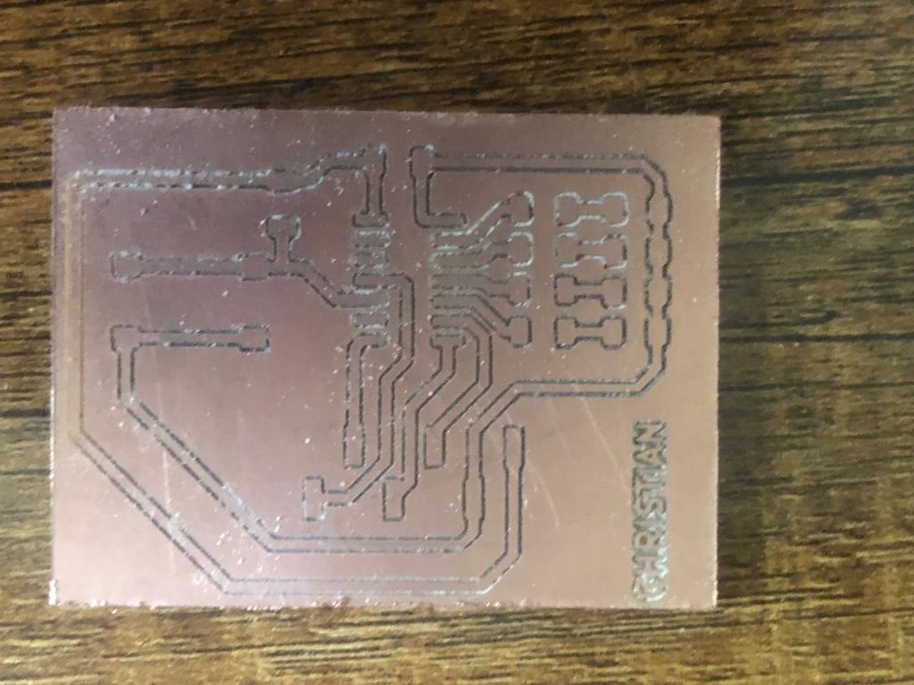
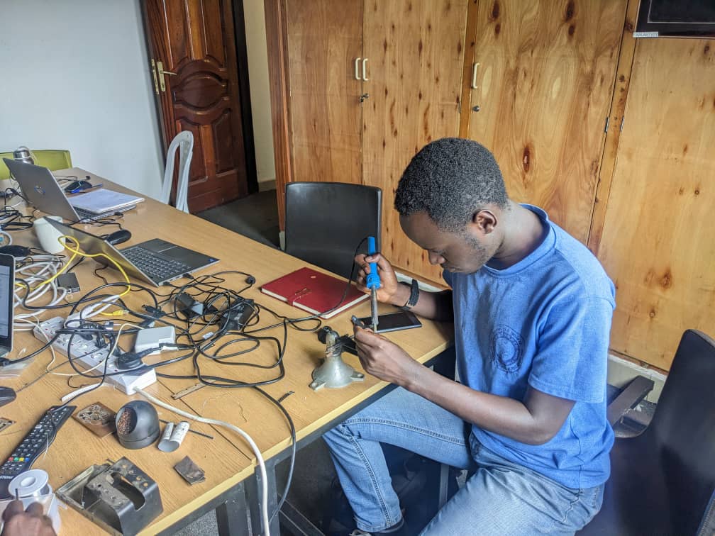
placed the components and started soldering on pcb which was hard to do because i realised that the clearance between copper traces
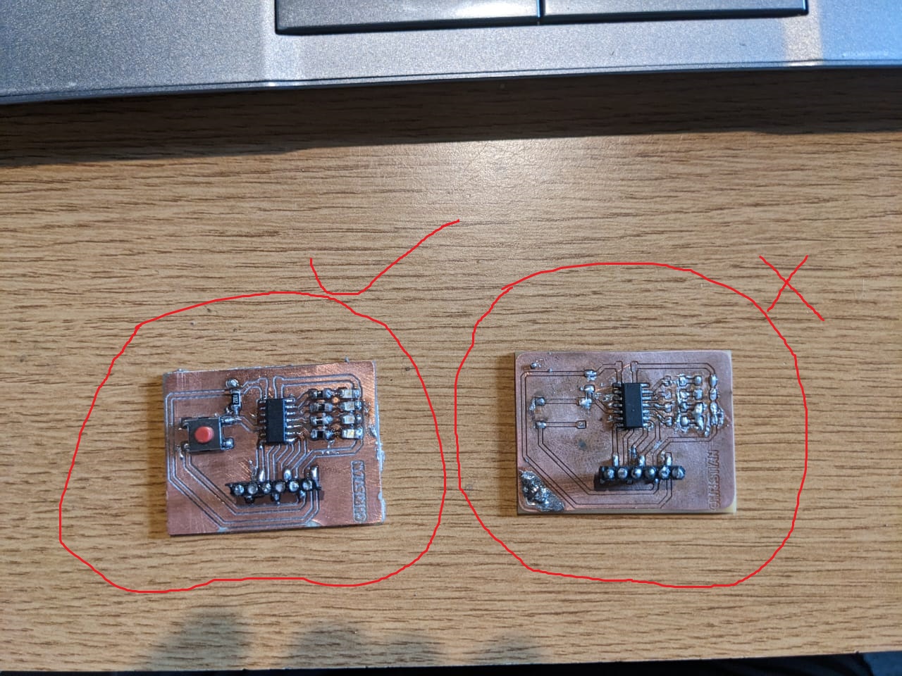
was too small and this created mess when soldering and created the short circuit due to small gap clearences so this pcb failed i was not able
flash into firmware because signal traces were shorted together.
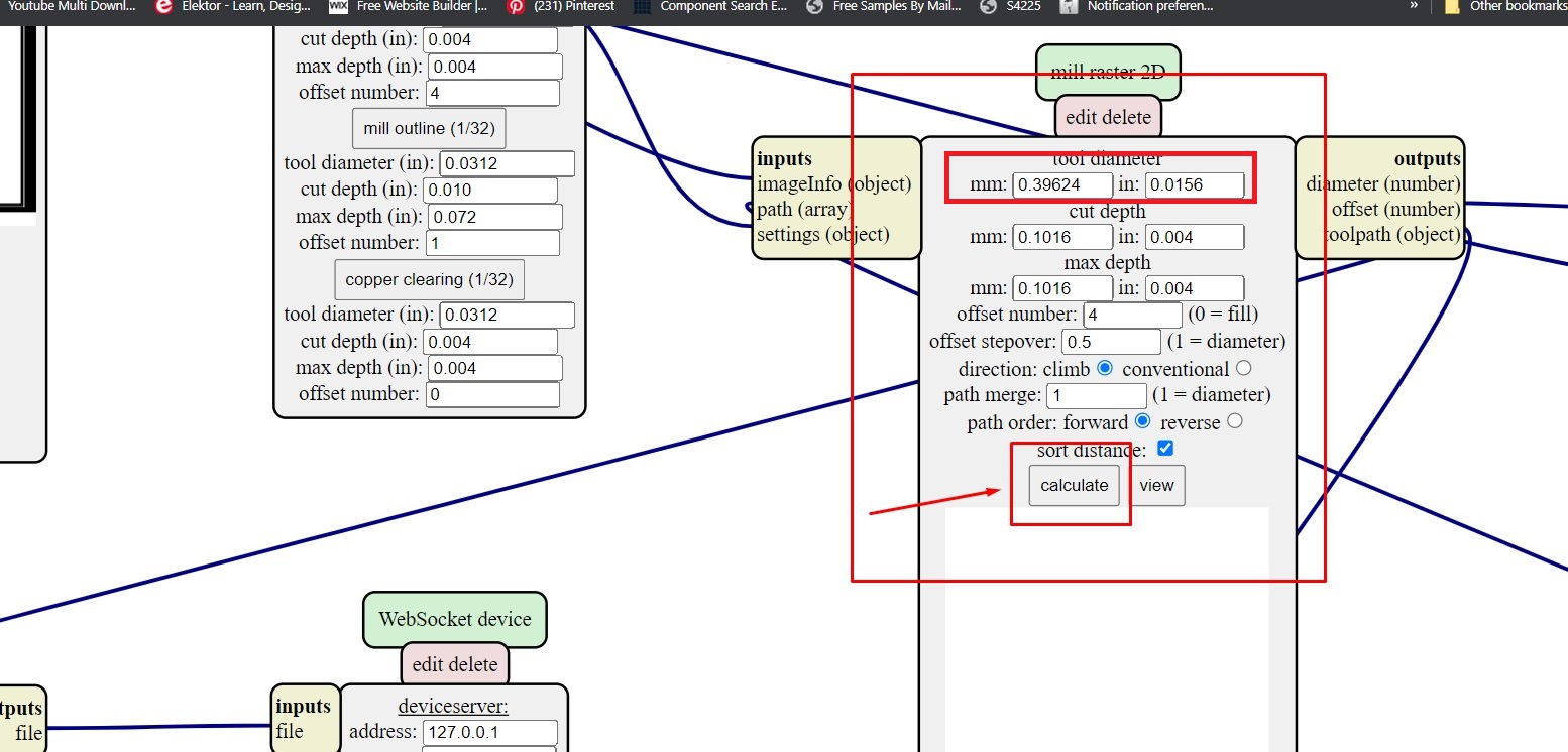
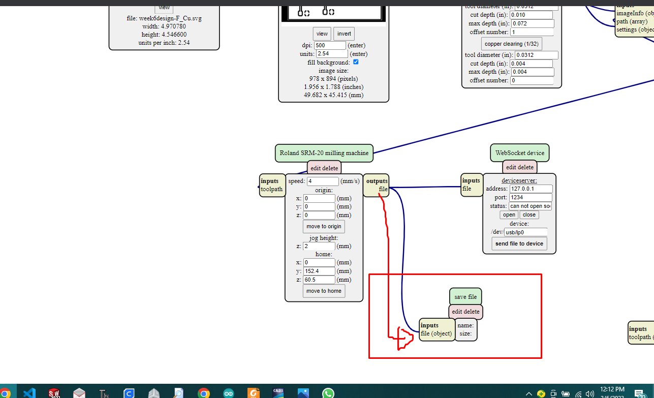
i made these mistakes during generating G-code where offse was 1 and the mill pass in it at once
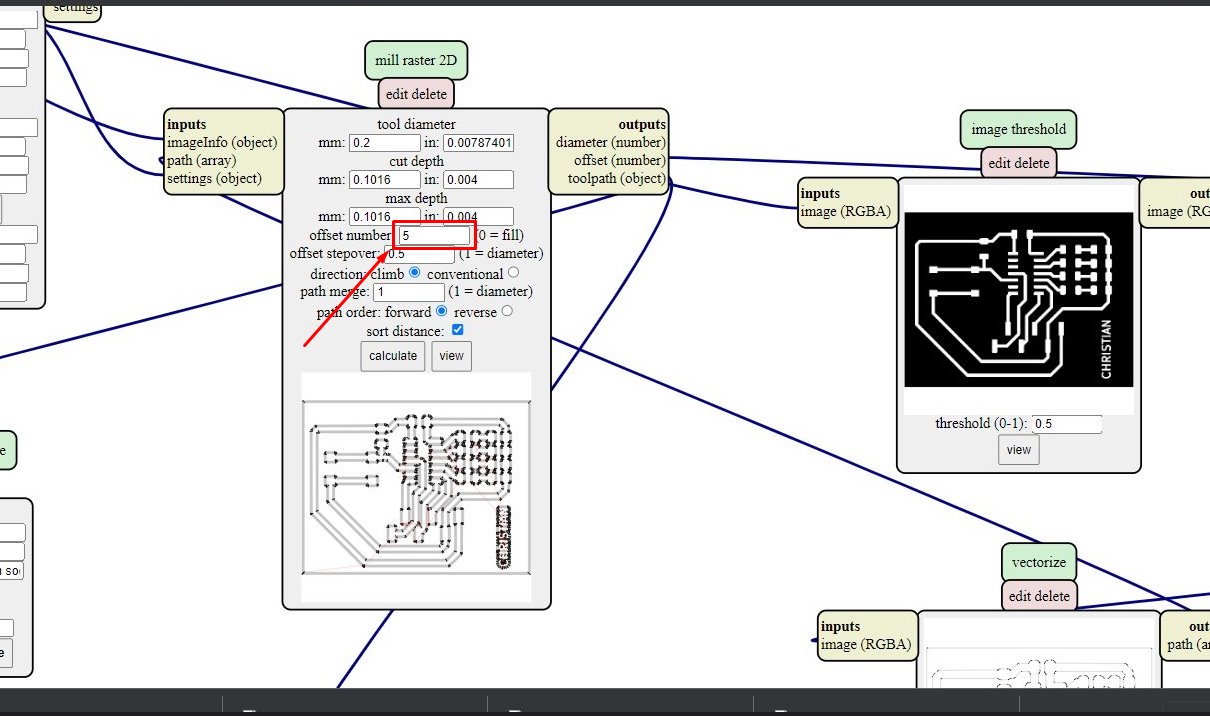
in shown image above offset there was 1 and i changed it to 5 to double the the tool path into 5 times
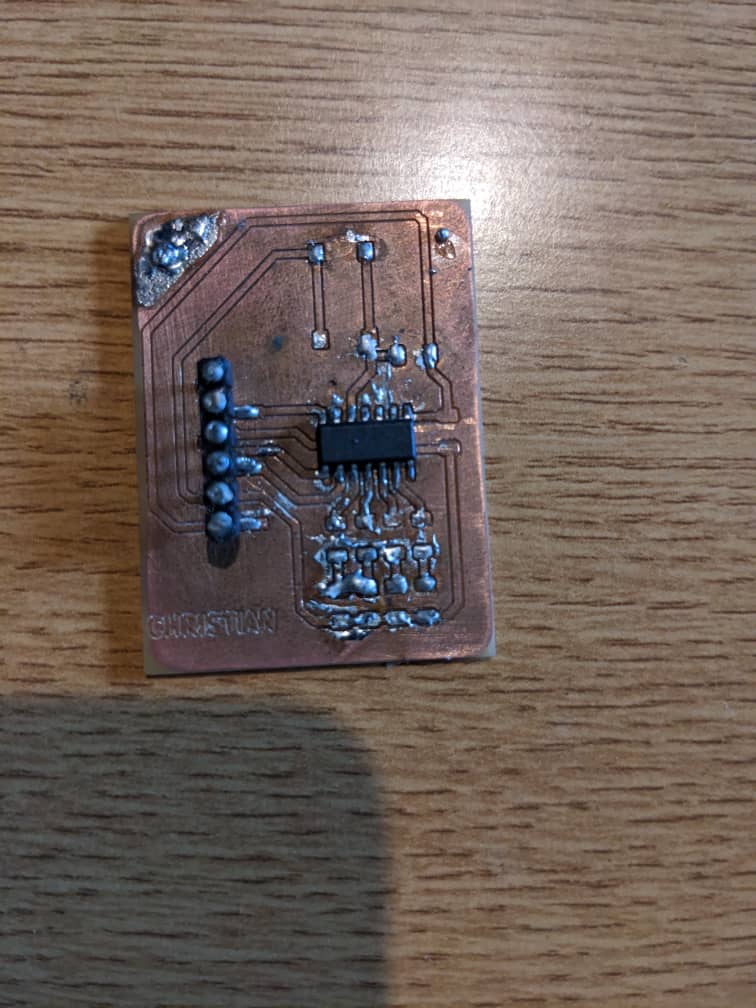
stepped again to the machine and make another pcb

i started soldering new components ATTINY44, button, LEDs, resistors.
here's two different boards and then i flash firmware into the ATTINY44 microcontroller
how i flashed the microcontroller
first of all we need to make communication between computer and microcontroller as my ATTINY44 doesn't have usb interface
which computer only has, so we need to find a way to make this communication possible
i didn't have avr programmer so i have another microcontroller as arduino that we could use to program the ATTINY44
here are the steps to program the microcontroller
open arduino locate to file>>preference>> add this link
https://raw.githubusercontent.com/damellis/attiny/ide-1.6.x-boards-manager/package_damellis_attiny_index.json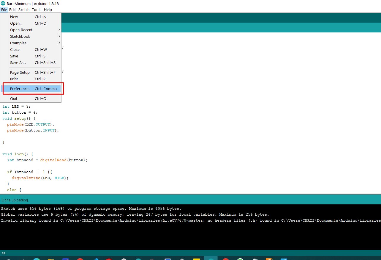
navigate to tabs tool>>boards>>boards manager
in searchbox search for attiny and click install it will directly install attiny package in arduino
after that navigate to tools>>boards>>attiny microcontrollers>>ATTINY44 which i have used
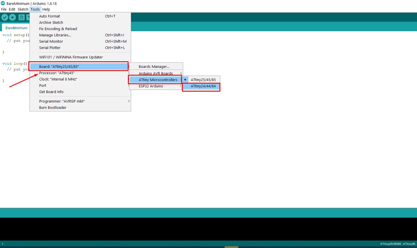
under board there is processor i choose ATTINY44
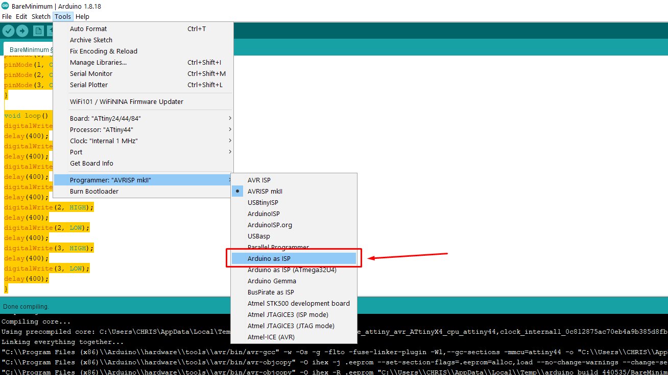
as i mentioned above i will use arduino dev board as programmer using spi communication
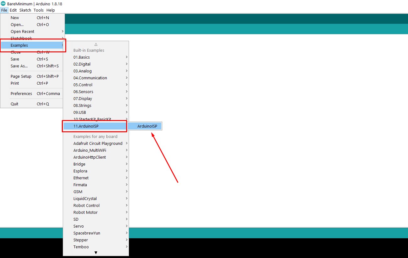
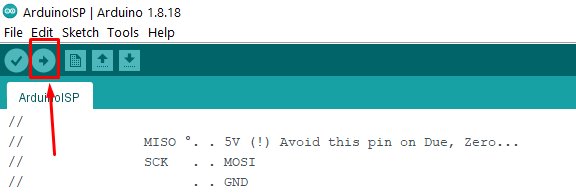
to do it navigate to files>>examples>>arduinoisp>>isp
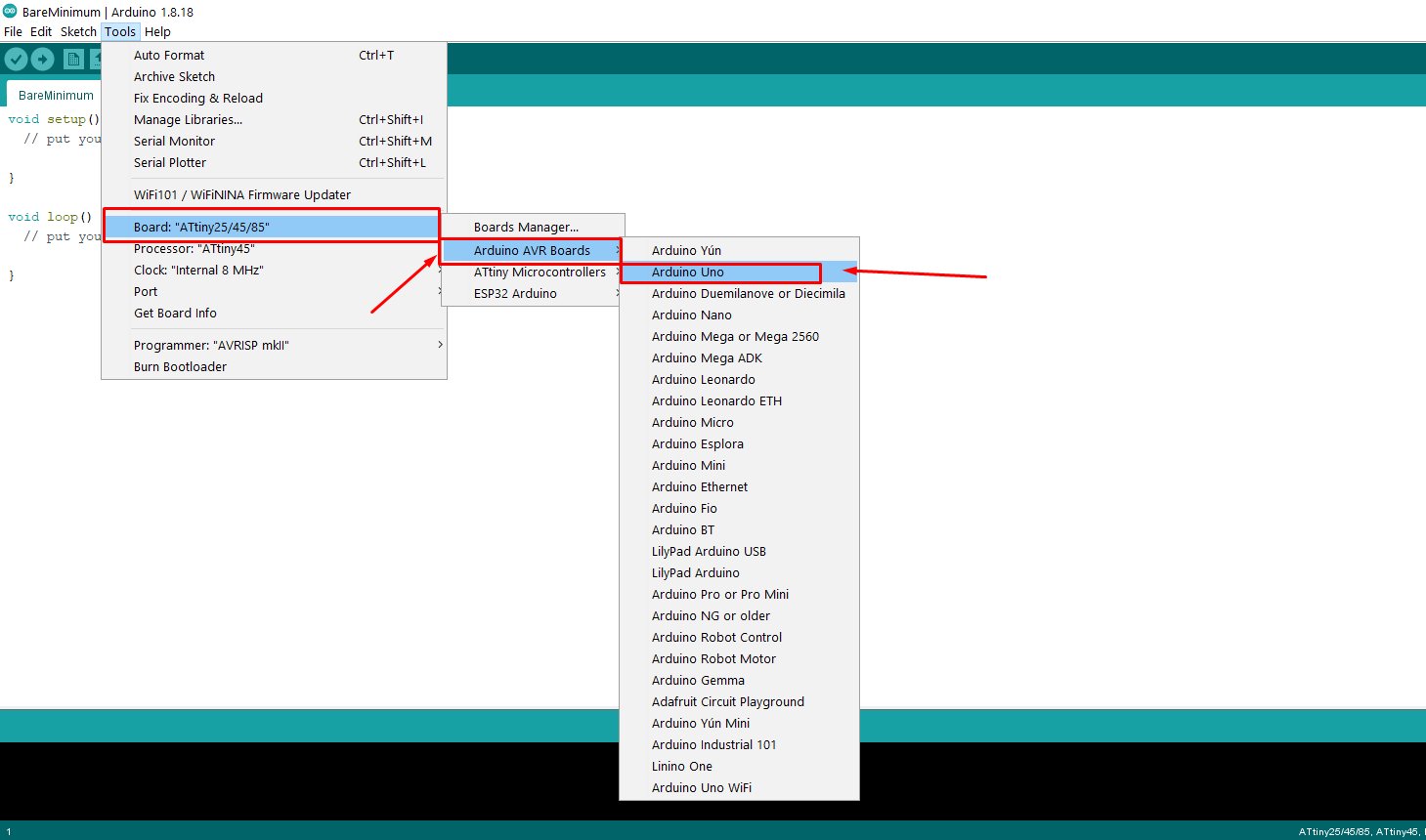
for my case i have arduino uno then to tools>>boards>>Arduino AVR boards>>arduino uno
here we are preparing programmer which we will use for pragramming ATTINY44
we upload arduino as isp
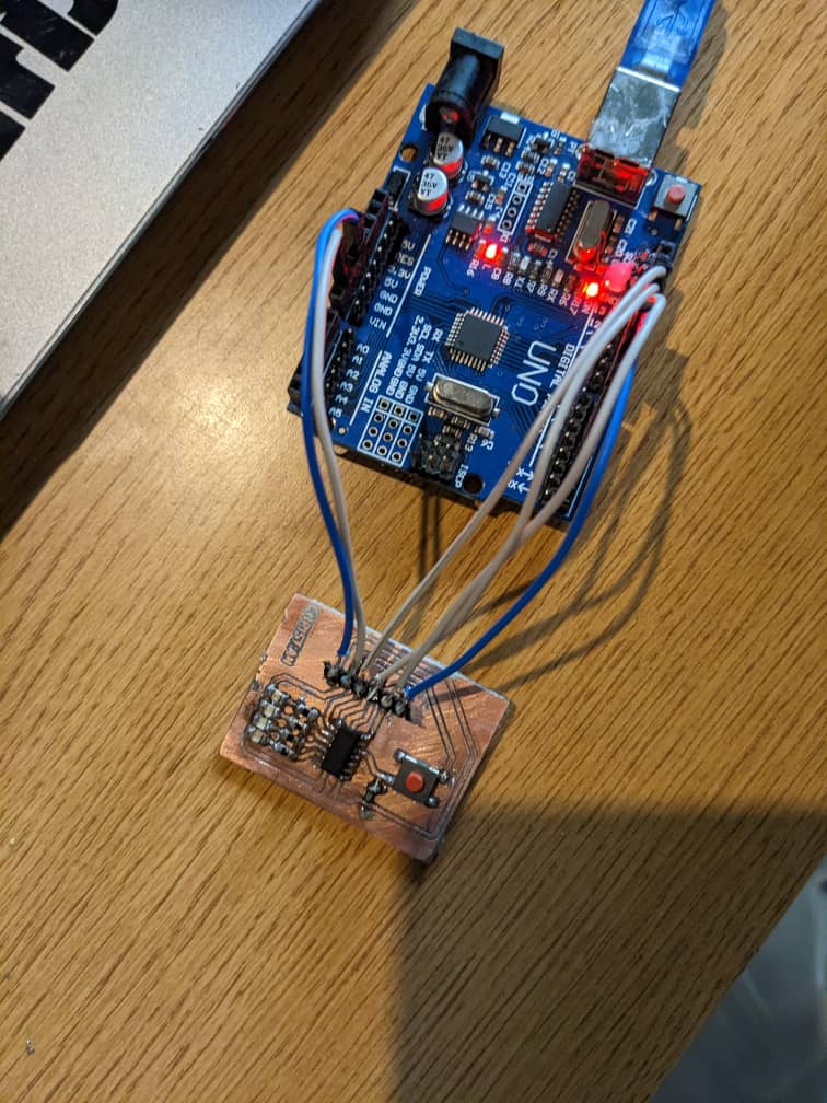
wiring arduino and ATTINY44 connection with spi communication
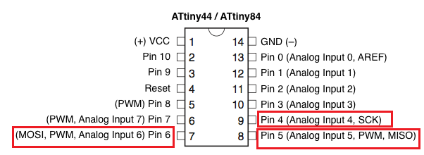
from ATTINY44 datasheet shows spi pins where we need MOSI,MISO,CLK
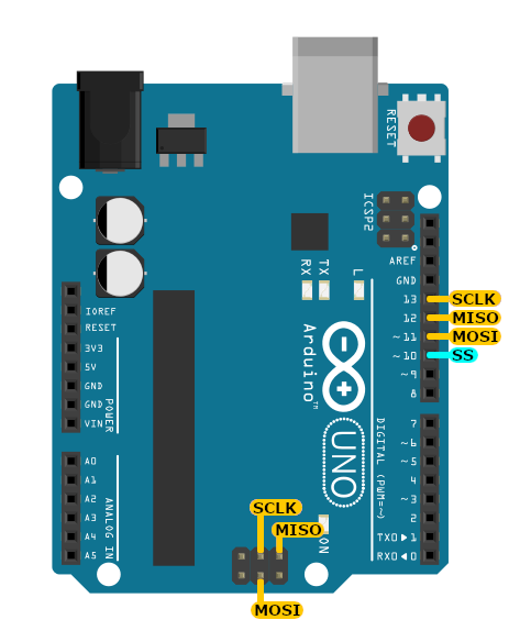
and also arduino has the same pins for SPI communication whose are assigned as shown
i connected it using the following conections
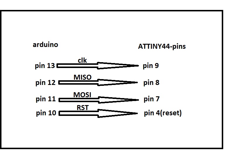
the connections shown in image below
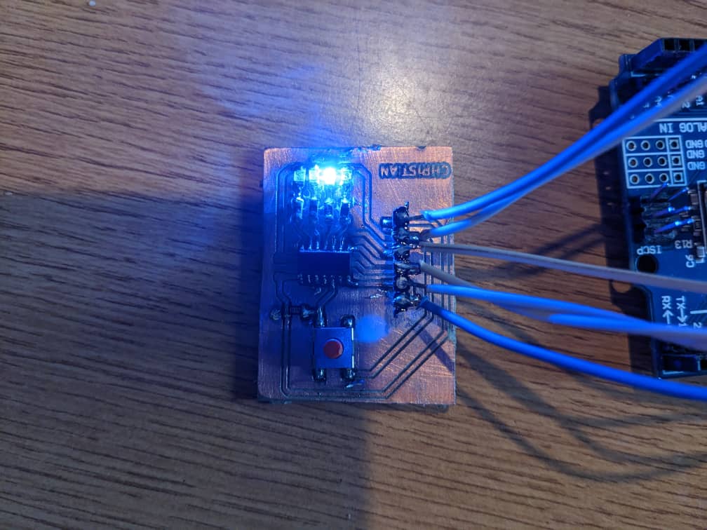
so i made simple codes to blink leds sequently
            void setup() {
              pinMode(0, OUTPUT);
              pinMode(1, OUTPUT);
              pinMode(2, OUTPUT);
              pinMode(3, OUTPUT);
              }

              void loop() {
              digitalWrite(0, HIGH);
              delay(400);
              digitalWrite(0, LOW);
              delay(400);
              digitalWrite(1, HIGH);
              delay(400);
              digitalWrite(1, LOW);
              delay(400);
              digitalWrite(2, HIGH);
              delay(400);
              digitalWrite(2, LOW);
              delay(400);
              digitalWrite(3, HIGH);
              delay(400);
              digitalWrite(3, LOW);
              delay(400);
              }
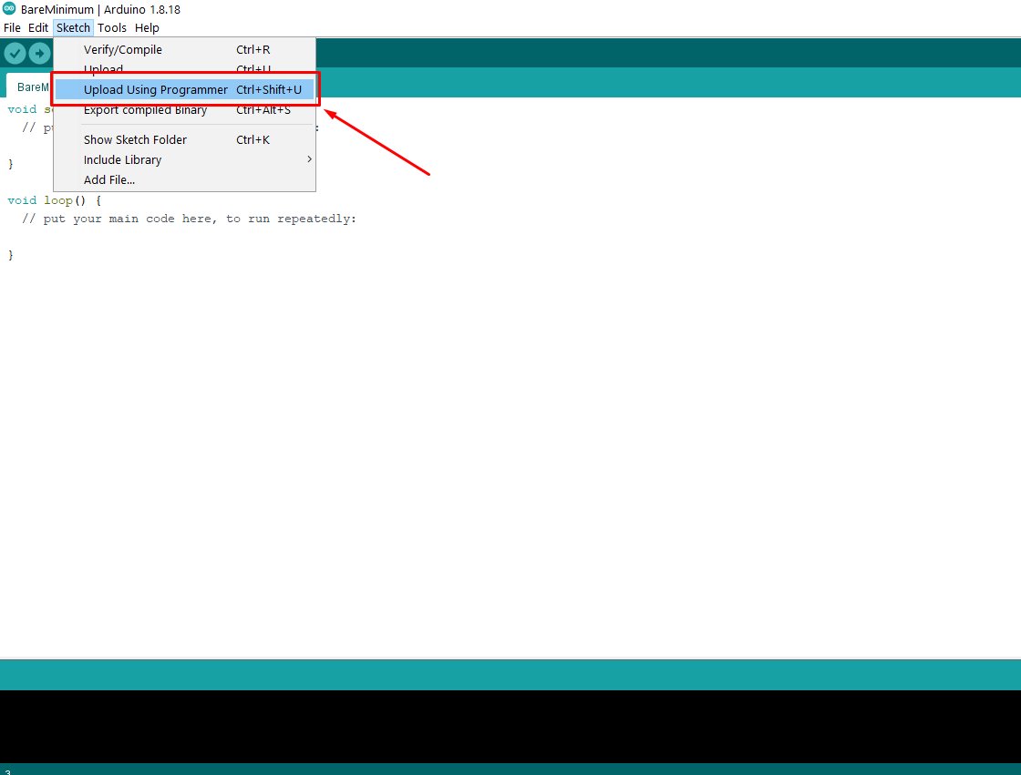
and then sketch>>upload using programmer
then the output went successfully the blinking was nice and no short circuit anymore
what i have learnt from electronic design
in this session of electronic design helped me to be familia with electronic CAD design such kicadmaking pcb and designing schematic of a project,
and also i have learnt to program a microcontroller usiing another type of board as well as new microcontroller interface