Team work
In the group assignment we had to carry out the characterization of the design rules and that we learned to use the mini router. My colleague Favell used the MODS program to generate the code. What I liked about this program was how accessible it is when uploading and downloading the file. In a group we saw how to use the machine.


First
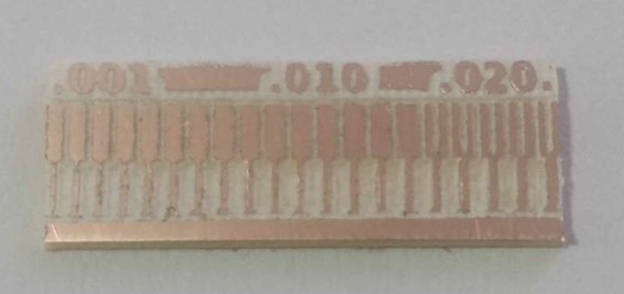
The path and gap ranges change from 0.001 to 0.02in, having an ideal of 0.016-0.001in, in this case because it is my first PCB I will use a higher range.
Taking into account the design guidelines. Also the components will have enough separation area so that when I solder it it will be easier for me (due to my little experience in it).
The equipment to be used this week will be: Fusion 360 software, Mods and Candle CNC, In general I will use: Mini CNC Router 3018 pro, Soldering station and DM3 digital microscope.

Export
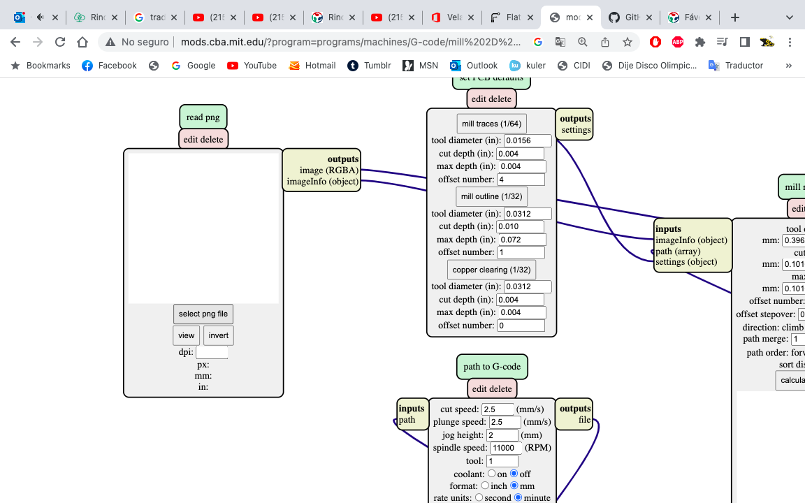
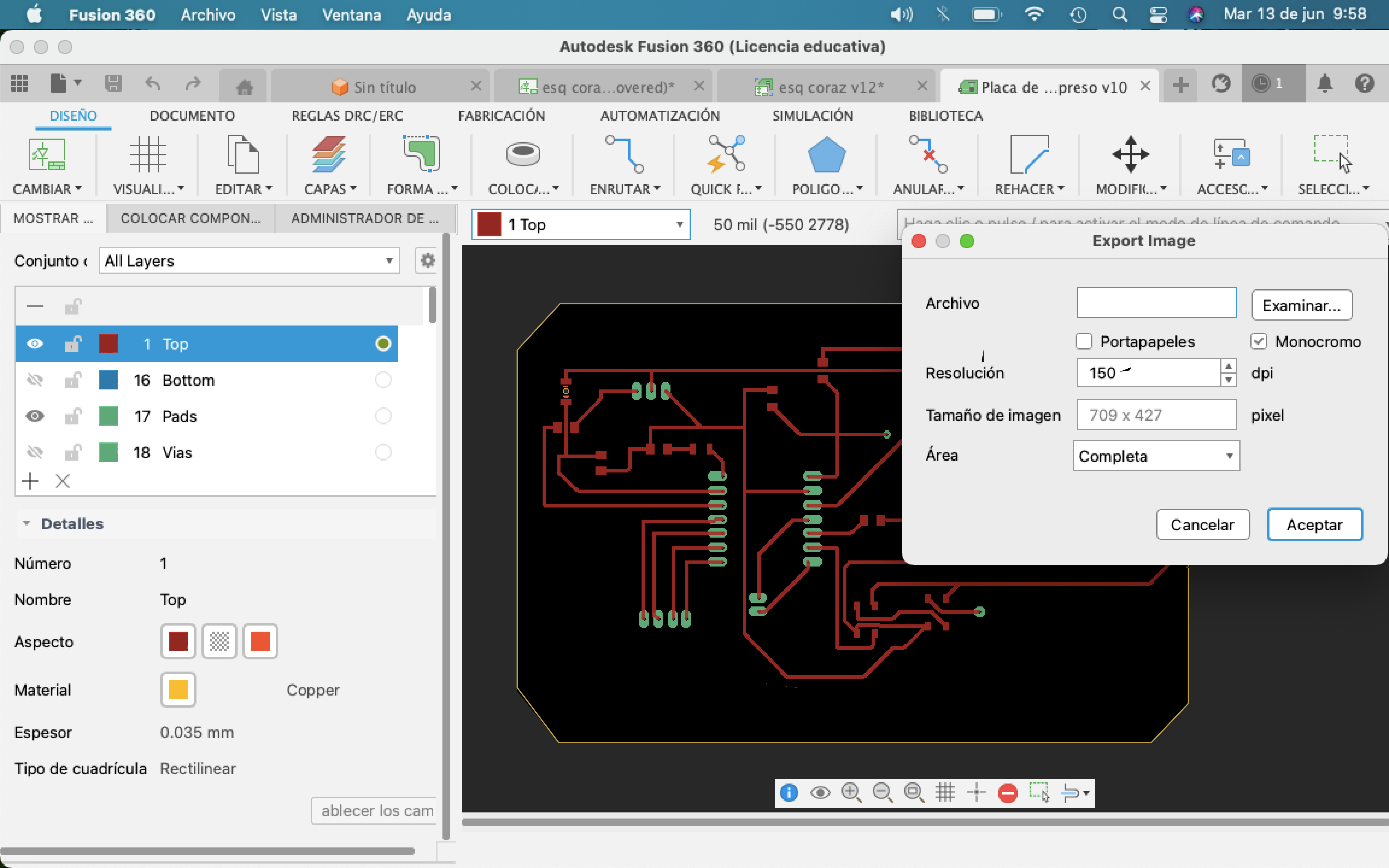
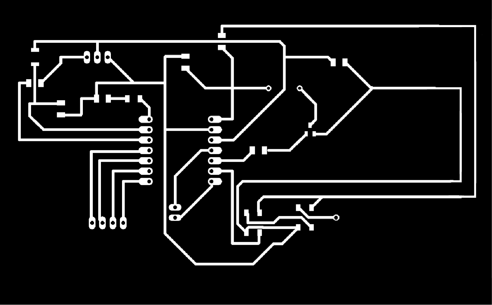
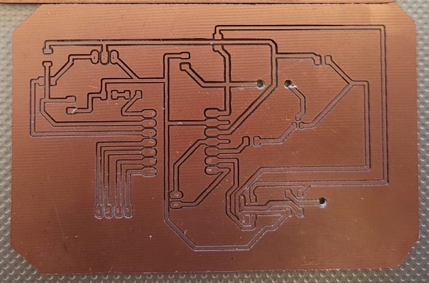
Previously, in my week 6, I designed a PCB in fusion 360 that we exported as a high quality image, we will use this image to continue with MODS and generate our "G code".
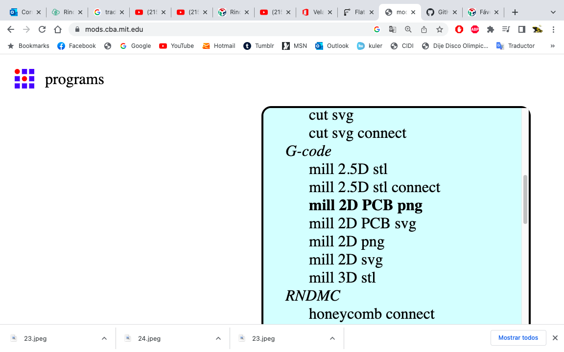
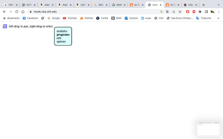
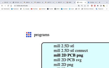
MODS
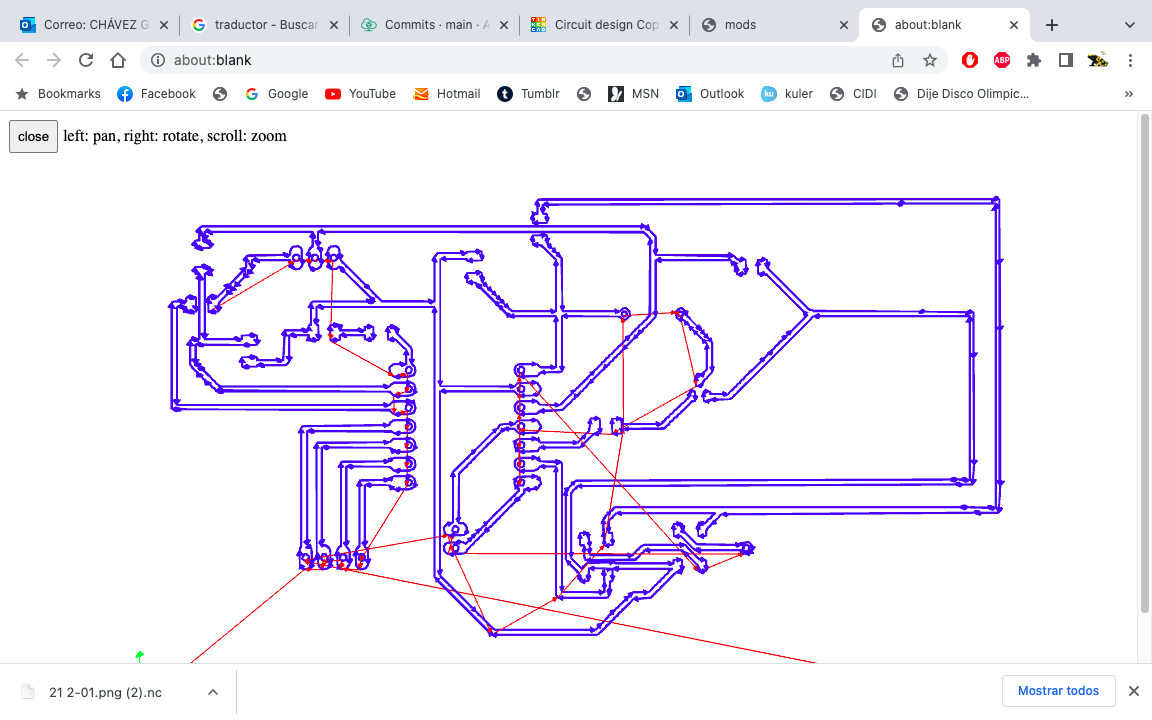
In MODS I opened the web page, and select the option PROGRAMS>OPEN SERVER PROGRAMS>MIL 2D PCB PNG.
You go to the MODS tutorial page to check the steps or for more information

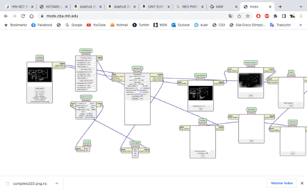
In the first section, place my image that I made in Fusion 360. And in the next box are the ranges to modify the cutting tools.

My laminate thickness is 0.0629" or 1.6mm, with a limit of ±0.13mm, the copper layer is 0.5oz, 0.7 mils, so I will use a depth of cut of 0.012", this drills to the 0.5oz.
In the SET PCB Default module, you can modify the diameter of the tool, the depth of cut and the number of passes. In the PATH TO G CODE module, you can edit cutting speed, RPM, and tool number. In the end, you only click on the calculate button and it generates an "nc" file.


.nc)
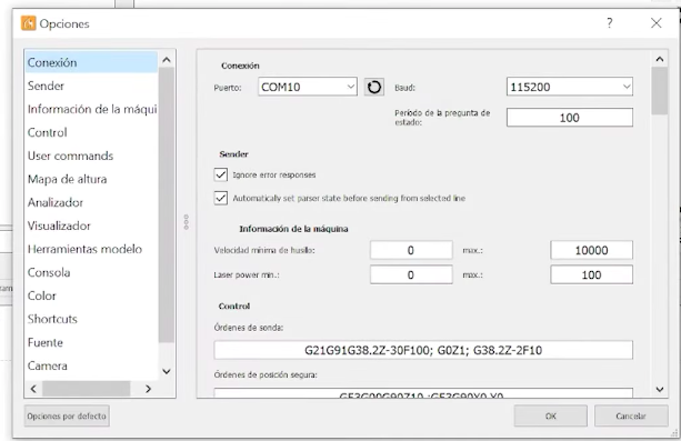
Candle
The Candle software is free to use and easy to communicate with the router. In this image we can see the description by areas of the program.
Step one, test the port, you go to service> options and look for the connection port with the machine.
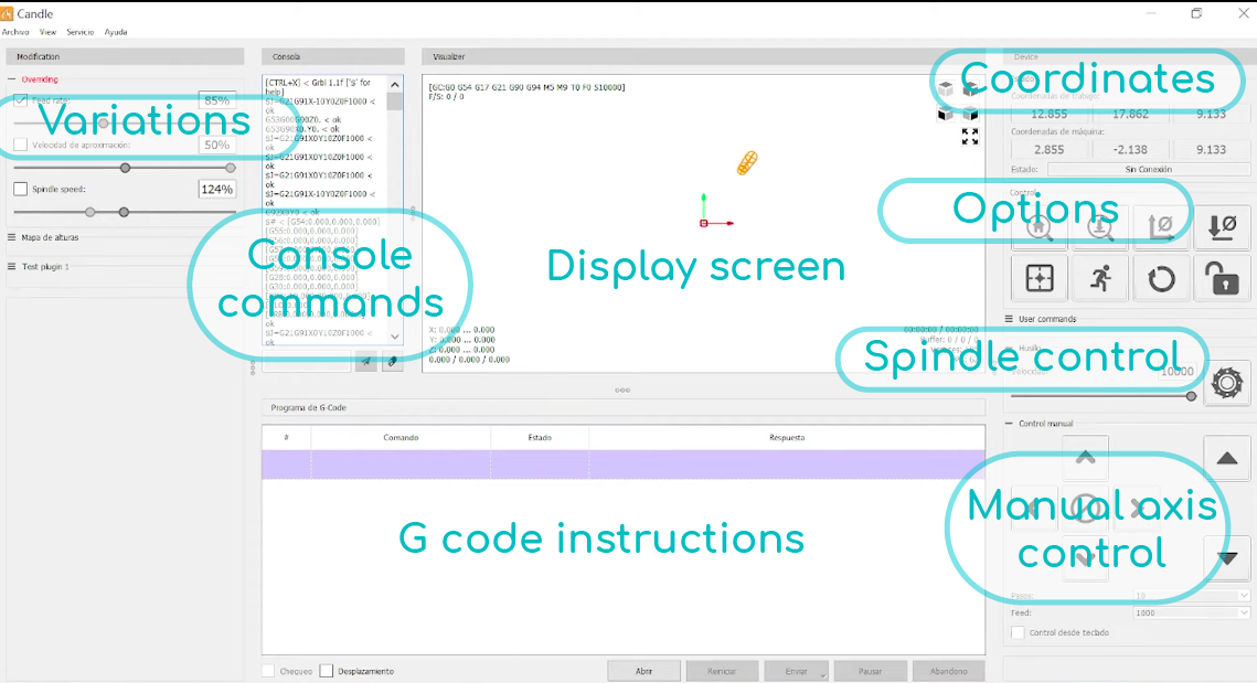
Step 2, open the "g-code" in File>Open.
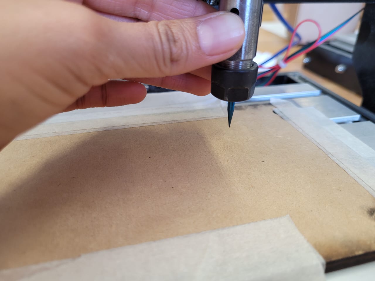
Step 3, Place the V-cutter and place the plate with double-sided tape.
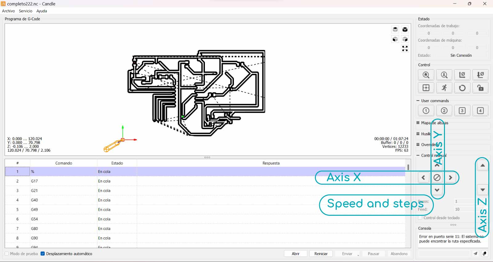
Then set the working zero, with the arrows on the X, Y & Z axis.
The zero reset button will allow you to return to zero. The safe position button will be activated when the cutter is finished (you can change it in options), the reset button is used to restore the work, the block and unlock button will help you stop and continue the work in any case.
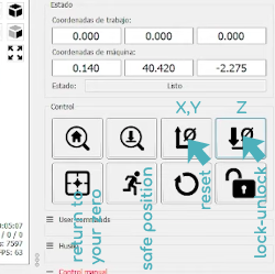
Once you arrange the elements, you can use the lower section and click the "send" button to start machining, you also have the pause and abandon button.
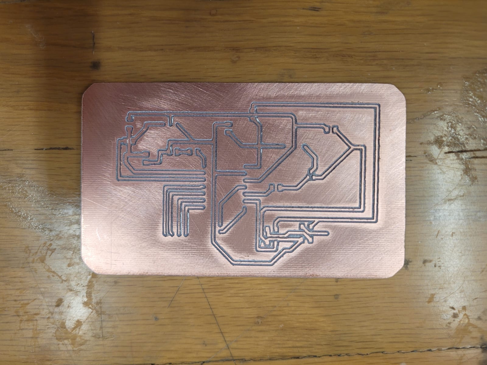
The same process will be repeated for the contour part, but in this case you must lower the cutter through the thickness of your plate, so that it can perforate.
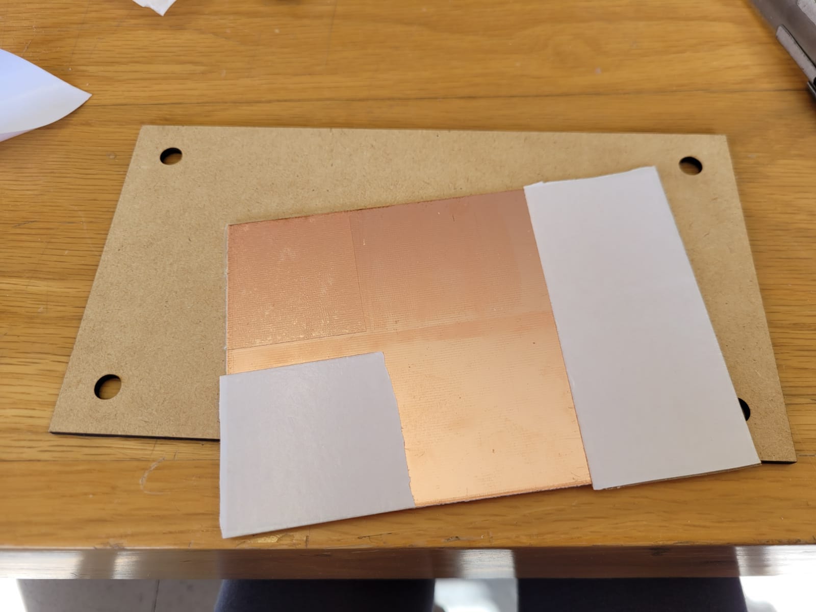
I decided to sand down my plate a bit, to prevent it from having raised corners.
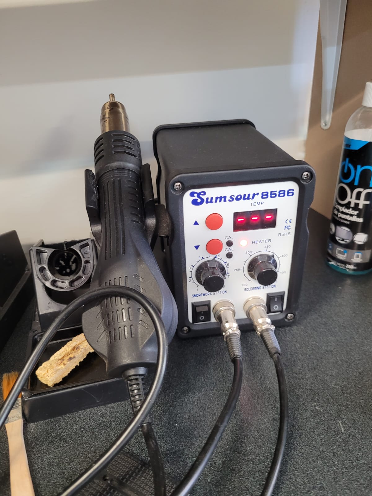
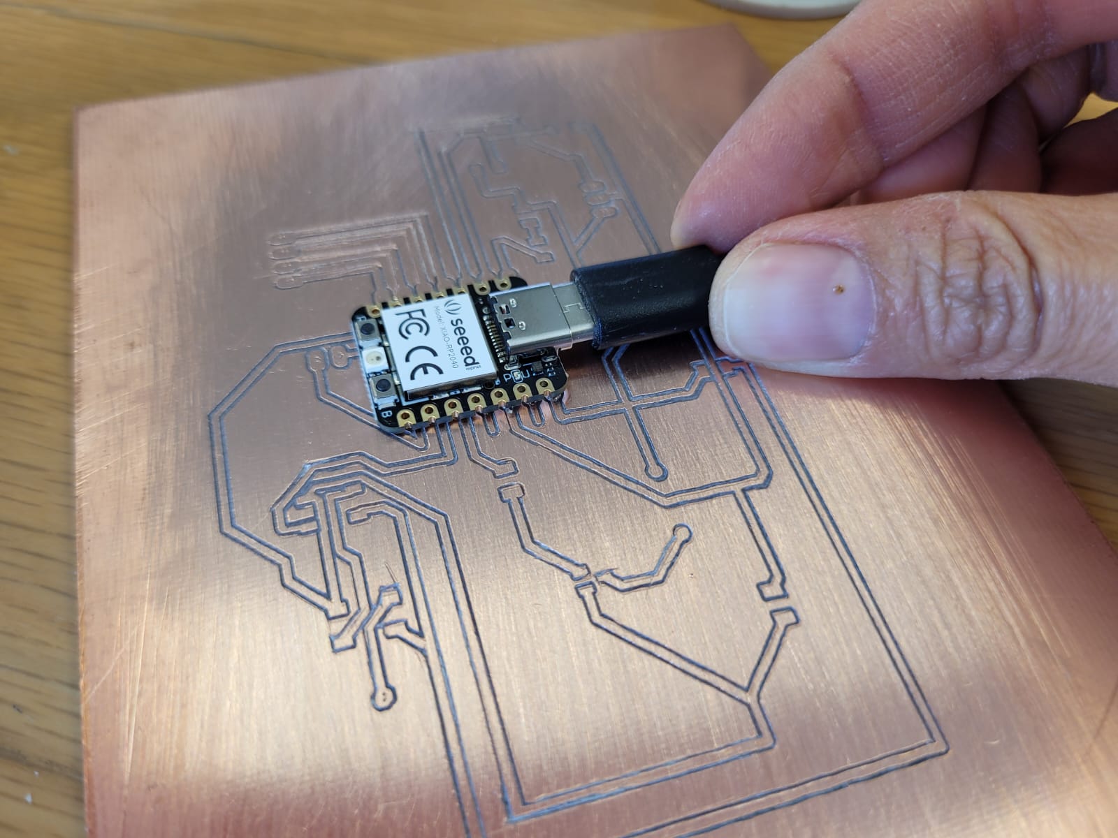
Since it was my first time soldering, I was practicing on various boards. Then I realized that I had not exported the version where I had the space for the connection of the components and I redid the board.

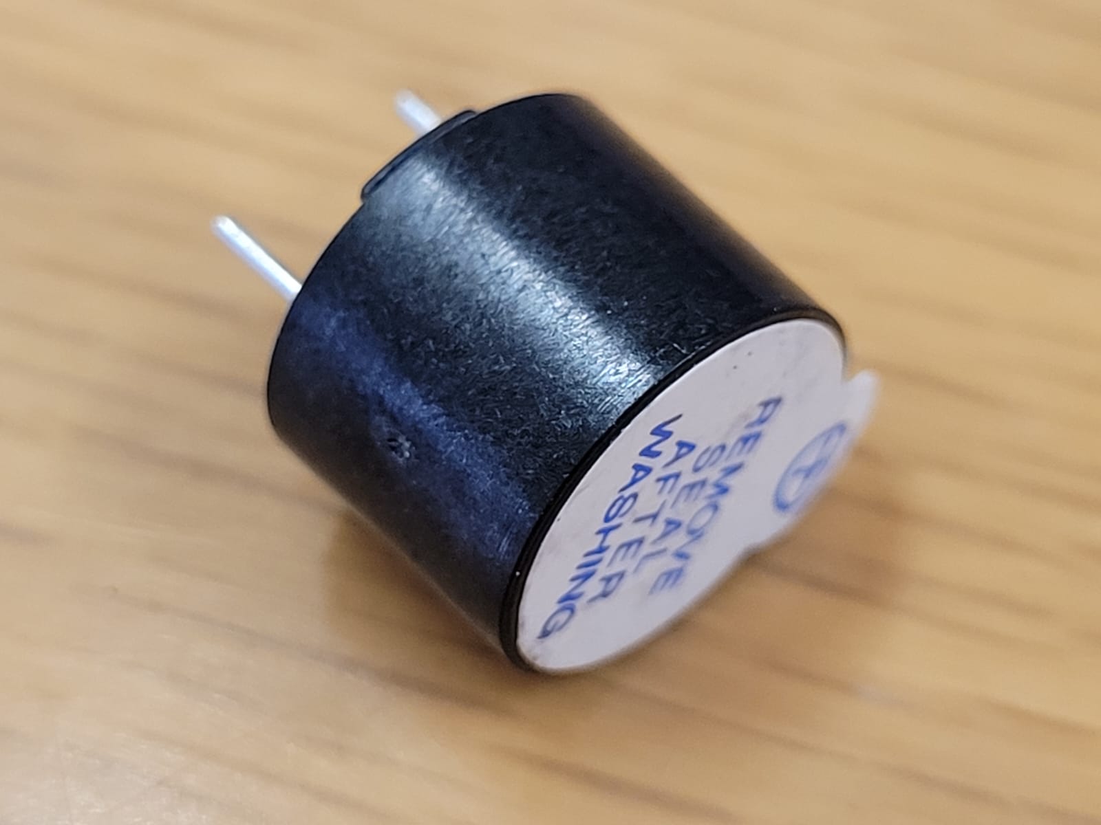
I used the list that I generated in week 6, and I gathered the components to solder them one by one, I will leave the largest components at the end except the xiao to check their space on the pcb.

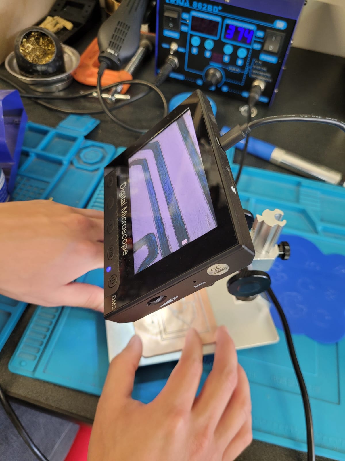
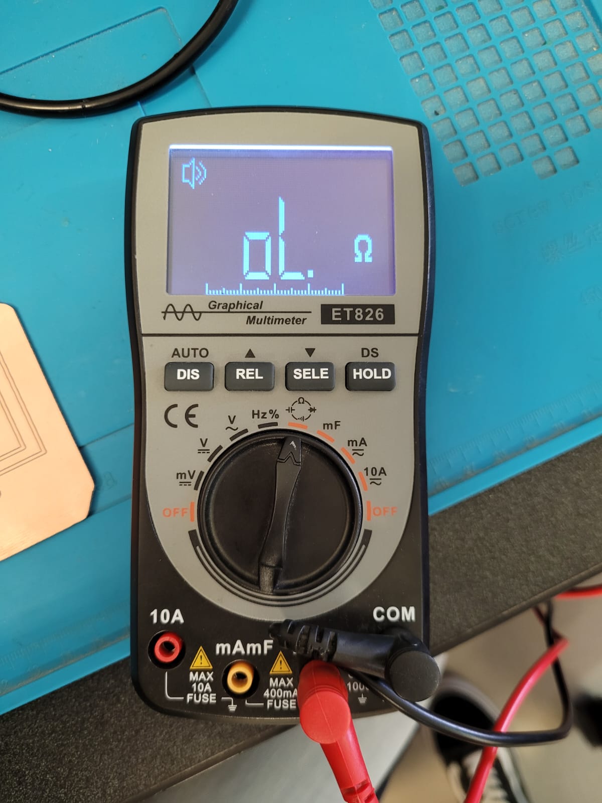
The multimeter helped me verify that there were no crosses and the digital microscope helped me verify where I could have excess solder.
List
| Part Value | Device | Package | Description |
|---|---|---|---|
| C1 0.1UF | C_CHIP-1206(3216-METRIC) | CAPC3216X135 | Capacitor - Generic |
| C5 0.1UF | C_CHIP-1206(3216-METRIC) | CAPC3216X135 | Capacitor - Generic |
| D2 1655 | 1655 | LED_1655 | Ws2812b 5050 Rgb Led / Adafruit Industries 1.6 mm |
| D3 1655 | 1655 | LED_1655 | Ws2812b 5050 Rgb Led / Adafruit Industries 1.6 mm |
| D4 LED_RED | CHIP-FLAT-G_1206 | LEDC3216X75N_FLAT-G | RED |
| JP1 PINHD-1X3/90 | PINHD-1X3/90 | 1X03/90 | PIN HEADER |
| JP2 PINHD-1X1 | PINHD-1X1 | 1X01 | PIN HEADER |
| JP3 PINHD-1X4/90 | PINHD-1X4/90 | 1X04/90 | PIN HEADER |
| JP4 PINHD-1X2/90 | PINHD-1X2/90 | 1X02/90 | PIN HEADER |
| LS1 AI-1223-TWT-12V-R | AI-1223-TWT-12V-R | XDCR_AI-1223-TWT-12V-R | BUZZER |
| Q2 NPN | NPN_SOT23-BEC | SOT95P237X112-3N | NPN - Generic TRANSISTOR |
| R1 R-US_CHIP-1206(3216-METRIC) | RESC3216X70 | - | Resistor Fixed - ANSI |
| R2 1001 R-US_CHIP-1206(3216-METRIC) | RESC3216X70 | - | Resistor Fixed - ANSI |
| R3 3000 R-US_CHIP-1206(3216-METRIC) | RESC3216X70 | - | Resistor Fixed - ANSI |
| R4 000 R-US_CHIP-1206(3216-METRIC) | RESC3216X70 | - | Resistor Fixed - ANSI |
| R5 000 R-US_CHIP-1206(3216-METRIC) | RESC3216X70 | - | Resistor Fixed - ANSI |
| S1 B3U-3000P(M)-B | B3U-X000B3U3000P(M)-B3000P(M)-B B3U-3000P(M)-B | - | Ultra-small Tactile Switch |
| U2 XIAO-THRUHOLEHYBRID-SMT-THT | XIAO-THRUHOLEHYBRID-SMT-THT | XIAO-GENERIC-HYBRID-MODULE14P-2.54-21X17.8MM | Seeed Studio XIAO Series Through-hole |
It was easier for me to place the soldering first and then the components, these were very small and I did not have much experience, but I placed them calmly.

It was quite difficult and I appreciate that my instructor told me to do the thick lines.


Neopixel Programing
To verify the board, place a small program with the neopixels so that it turns purple, remember that you must integrate the adafruit library and the xiao library to do so.
I started by programming the neopixel to turn on and off, first integrating the Adafruit library: https://learn.adafruit.com/adafruit-neopixel-uberguide/arduino-library-use

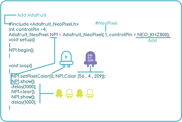
      #include Adafruit_NeoPixel.h //add the symbols from the image above

      Adafruit_NeoPixel NP1 = Adafruit_NeoPixel( 1, controlPin + NEO_KHZ800);
      void setup()
      {
      NP1.begin();
      pinMode(1, INPUT);
      }


      void loop()
      {

        NP1.setPixelColor(0, NP1.Color (56 , 4 , 209));
        NP1.show();

        delay(1000);

        NP1.clear();
        NP1.show();

        delay(1000);

      }
Video
This week was very diverse, in my first experience welding I can tell you that I liked it, but I lack practice.