9. Output Devices
Refer to the following link to see how my group characterized the output power of a DC motor across different voltages.
This week I wanted to experiment with creating a standalone DAC using an ATTiny1614. I want to use the 1614 because of its small size, and having 12 available pins to make the DAC. 8 will need to be dedicated to the DAC - giving it a resolution of 8 bits. To make a DAC is pretty simple - but uses a lot of pins. It essentially consists of a voltage divider with 8 single-valued resistors (doubling the voltage each time). We can assign the resistor with lowest voltage to represent the least significant bit of an 8-bit analog number. The highest voltage, will represent the most significant bit. The output is connected to the top of the voltage divider, and uses the summation of voltages in the divider to adjust the voltage at the output.
| Design File Links |
|
|---|---|
| - ATtiny1614 DAC KiCad Schematic |
|
| - DAC Binary Counter Test Code |
|
|
-
Gerber Copper Traces
- Gerber Edge Cuts |
|
Initial Design and Simulation
|
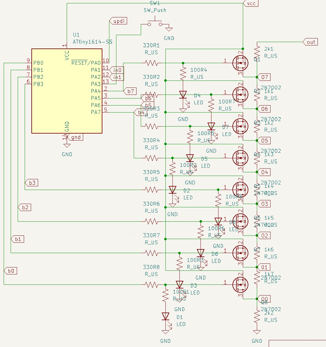
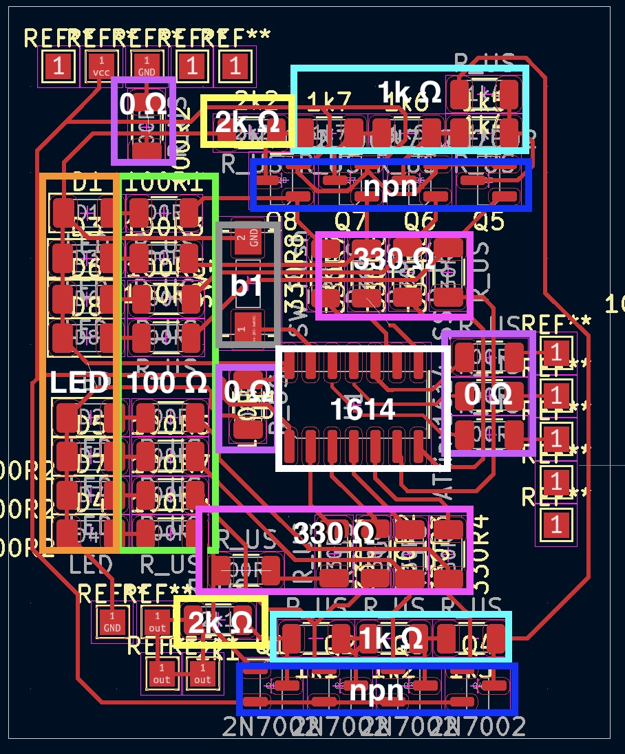
This design consists of a voltage divider with 8 separate voltage reference values, each wired up to the source of different npn transistors.
The gate of each transistor is connected to a pin of the microcontroller. To represent a value in binary, we just need to turn on the transistors in order of least voltage to greatest.
The lowest voltage will represent a value of 1 in binary, and the highest voltage value represents 128 in binary.
If we wanted to represent a number in binary, we just turn on the corresponding pins for each bit.
So for example, if I have a 4 bit DAC, with 4 different voltage values (1.2V, 2.4V, 3.6V, 4.8V) here is how we could represent different values:
DAC PINS: [pin1, pin2, pin3, pin4]
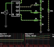
It is important to test this theory before attempting to build the circuit. I was not totally sure which value resistors I wanted to use, so this would be a good opportunity to figure that out. Using Falstad, I created a simple schematic using a voltage divider and observed the voltage value when different gates are active. Here, I used a binary counter in place of a microcontroller, to test each step up in voltage. I also scaled back to 4 bits for this test, since 8 bits really just involves some replicated circuitry. From the video, you can see that we get a successful step-by-step increase on the voltage of the output! I found that changing the values of the resistors didn't really impact the output much, so long as the values weren't too high, and we kept them all the same value. I ended up sticking with 1k Ohm resistors for the divider, with 2k Ohm resistors on each side (output and ground). |
Designing the Schematic
Version 1: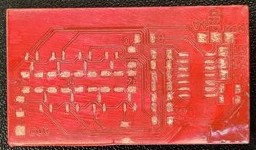
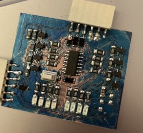
My first board consisted of the same setup of the final board, minus the indicator LEDs. This board is composed up of the voltage divider, npn transistors with their gates wired up to the 1614 pins, and the output. While debugging the first iteration, I was only getting an output that was either high or low, rather than a non-box shape like an AC signal would be. Version 2: 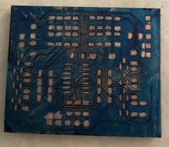
Debugging via the oscilloscope led me to adding the indicator LEDs for easier and more intuitive debugging. Each LED is wired directly to each pin of the 1614 via a 100 ohm resistor. This way, each LED lights up with each corresponding 1 digit in the binary number output. |
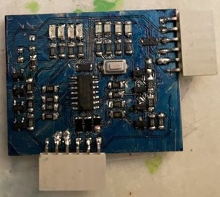
Final Schematic
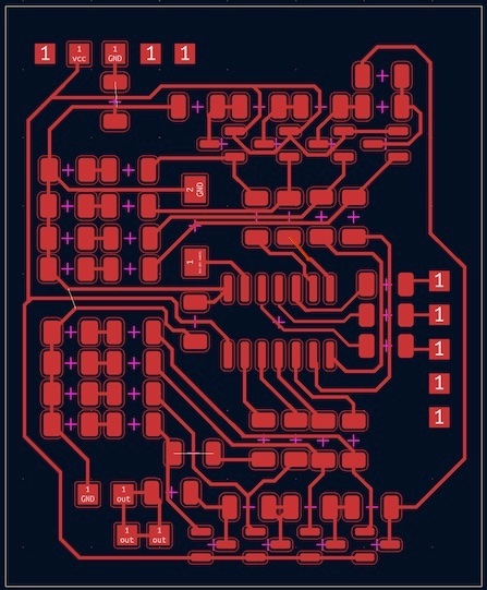
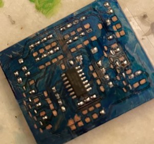
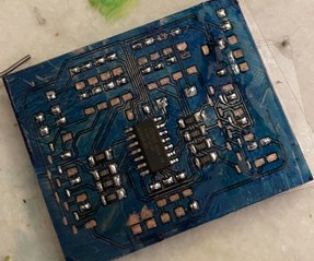
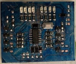
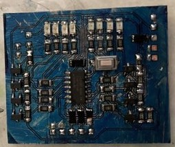
Final PCB vs. Labeled PCB (Final)
|
| Constructing, Programming and Testing the Board |
|
|---|---|
|
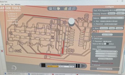
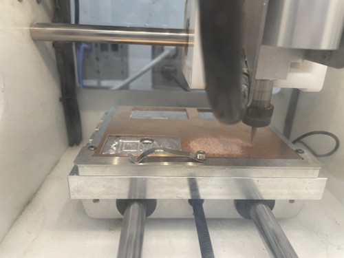
To mill my board, I used a 20˚ 0.1mm V-bit. As you can see in the image on the right, there are some traces that could not be milled due spacing being too close.
To fix this, I ended up spacing the traces a little farther in KiCad.
But for the first board, I ended up just running an Xacto knife between them to hand-cut the traces.
This isn't ideal, but it worked fine for that board.
My final board uses the better spaced traces.
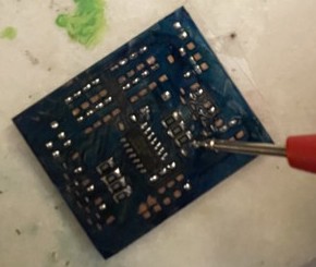
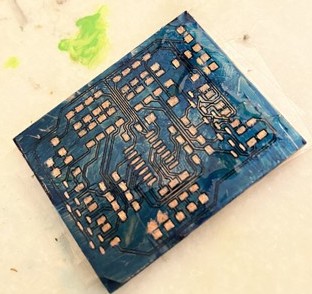
After milling my boards, I did a continuity test, to make sure there weren't any shorts. This consisted of taking a multimeter, putting one pin on the trace I was testing, and the other on varying spots on the board. It should only show continuity for wires that are connected by pure copper. After verifying there were no shorts, or recutting traces with the Xacto where there were traces, I added a solder mask on top. This makes the soldering process easier as it prevents solder bridges and decreases the chances a trace will rip off due ot heat. A few mistakes happened along the way. Firstly, I had an issue on one board having traces ripped off. To combat this, I adjusted my soldering iron to 650˚F, as opposed to the default 750˚F the Hakko irons come with. Having it too hot is fine with a well-made production board, but it totally obliterates handmade milled pcbs. Make sure to also periodically check the continuity of the board after soldering a handful of components. In the picture below, I am checking out the group of 4 resistors I had soldered. 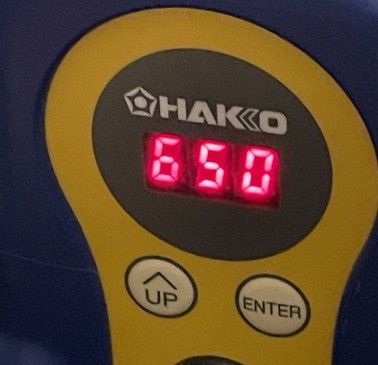
I found this process to be the most efficient, since it requires the least amount of debugging due to the repetitive testing. If it worked 5 minutes ago before you soldered a resistor on there, odds are likely that the action of soldering that resistor is what caused the issue, and gives you a great place to start. |
|
|
Soldering Process |
|
|---|---|
| I started by taking my UV cured board, and scraping away the mask from the solder pads. |
|
| I then applied the flux contained within this ancient artifact from an earlier age, just by spreading it across the board. It did make the board sticky, but it will cleaned with alcohol at a later step. |
 |
| For each of the component trace pairs (or trios for transistors), I applied solder to one pad. This will make it so I just need to solder one side of the component by sliding it into the melted blob already on the trace. |
 |
| I started with the 1614, because it's the largest and most-middle component. Once I got it connected to the one pre-soldered pad, I just had to perfectly align the rest of the legs with the other traces, and then soldered them in. |
 |
| Followed by the output resistors (330Ω) which then connect to the corresponding switching transistors and the indicator LED. |
 |
| I then did a continuity test to make sure everything was connected properly. I repeat this step between each group of soldered components. |
|
| Then came one side of the transistors and the button. |
|
| I soldered the LEDs and their 100Ω limiting resistors. I used the diode tester on my multimeter to verify they all lit up in the correct orientation, BEFORE and AFTER soldering them in place. |
 |
| After one side worked, I soldered the other. |
 |
| Finally, I soldered the connector headers to interface with the device. |
 |
| Once the soldering and continuity testing was done, I cleaned the board using a tooth brush and isopropyl alcohol. This ended up removing a bit of the solder mask - most likely due to not being fully cured. I found the lighter colored solder masks had an easier time curing. |
 |
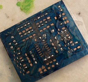
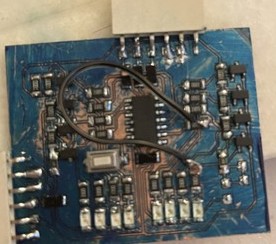
| Later on, I realized that I forgot to create a trace that connects one pin to its LED, so I just used a jumper wire to connect it. |
|
| Programming the Board Test |
||
|---|---|---|
| The goal of the test is to recreate the output as seen in the simulation video above. |
|
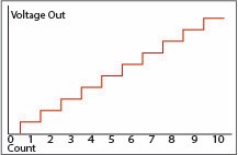
The simulation counts from 0 to 15 (4 bits), and raises the voltage at the output based on the counted value. |
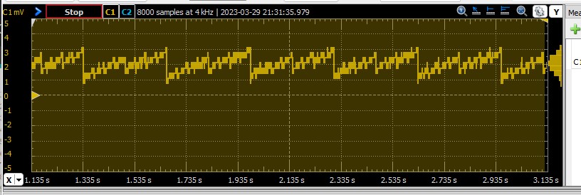
| For this test, we are going to make the DAC count from 0 to 255 (8 bits), so we can observe the produced voltage at all levels. Ideally, we should see a staircase waveform that increases a fixed amount per step. However, this assumes that we are running in ideal conditions where the voltage at each divider is a perfect double of the last. But, due to noise from the controller and power supply, inconsistent resistor values and general EMI, this is unlikely to run perfectly and will be noisy. Especially considering we don't have any filters or decoupling. |
|
|
|
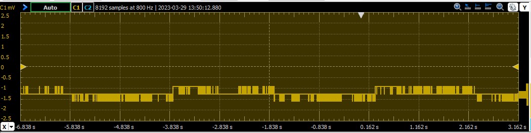
At first, I had written the code for it to count from 0 to 255, by turning on varying pins corresponding to each bit in the binary number. I wired it so it uses pins 0 - 7, to make the code easy to loop through. My first attempt was not successful, and was producing a weird output as shown to the right. To start, I tried to make a triangle waveform, by doing the staircase count forward, and then backwards when reaching the max. It seems to be a bunch of positive and negative impulses, which is definitely not the triangle waveform I was expecting. |
|
|
|
Well as it turns out, I had accidentally flipped the order of significant bits in my code. So once I looped backwards instead of forwards, it started to produce a respectable, albeit noisy, triangle wave. You can view the code for this test on the right: 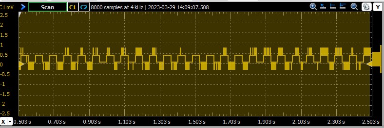
This seemed pretty good! Now to change the triangle wave into the staircase wave, I changed my void loop() to contain this code instead:
 void loop() {
   for(uint8_t i = 0; i < 64; i+=1){
     writeOutput(i);
     delay(5);
   }
 }
The delay causes there to be visual steps in the waveform that we can observe.
By not having the delay on the triangle waveform, it causes everything to happen very fast, which makes it harder to observe using my Analog Discovery 2.
Here is the output with the change to the code:
As you can see, it's not perfect. I think this is mainly due to the voltages not being perfect multiples, which you can see every time the 7th bit switches, there is a large jump in voltage potential. This one might have a higher magnitude of voltage attached to its resistor in the divider. |
//triangle wave test
uint8_t outputPins[8] = {PIN4_bm,
  PIN5_bm,
  PIN6_bm,
  PIN7_bm,
  PIN3_bm,
  PIN2_bm,
  PIN1_bm,
  PIN0_bm};
uint8_t* pinPortsOut[8] = {&PORTA.OUT,
  &PORTA.OUT,
  &PORTA.OUT,
  &PORTA.OUT,
  &PORTB.OUT,
  &PORTB.OUT,
  &PORTB.OUT,
  &PORTB.OUT};
uint8_t* pinPortsDir[8] = {&VPORTA.DIR,
  &VPORTA.DIR,
  &VPORTA.DIR,
  &VPORTA.DIR,
  &VPORTB.DIR,
  &VPORTB.DIR,
  &VPORTB.DIR,
  &VPORTB.DIR};


void initiatePinModes(){
  for(int pinNum = 0; pinNum<8; pinNum++){
    *pinPortsDir[pinNum] |= outputPins[pinNum];
  }
}

void writeBit(uint8_t srcValue, uint8_t bitPosition){
  if((srcValue & (1 << bitPosition))){
    *pinPortsOut[7-bitPosition] |= outputPins[7-bitPosition];
  }
  else{
    *pinPortsOut[7-bitPosition] &= ~outputPins[7-bitPosition];
  }
}

void writeOutput(uint8_t value){
  for(int pinNum = 0; pinNum<8; pinNum++){
    writeBit(value, pinNum);
  }
}

void setup() {
  initiatePinModes();
}

void loop() {
  for(uint8_t i = 0; i < 64; i+=1){
    writeOutput(i);
  }
  for(uint8_t i = 63; i >= 0; i-=1){
    writeOutput(i);
  }

}
|
|
End Results:
| Analysis:
|
Realtime:
|
Future Improvements:
Overall, I am pretty happy that I was able to produce a fairly good waveform, despite the limitations of my design. For the future, I would like to incorporate a few additional features into the circuit and code:
- Filtering and Decoupling Capacitors - to smooth the waveform.
- I2C Support - this would require programming I2C into the 1614, to read signals and then output the values received.
- Debug Button - I would like for the button to have the functionality to be pressed to run a test waveform.
- Multilayer PCB Design - adding a ground plane would help make the circuit smaller, easier to build, and hopefully help reduce noise.