6. Electronics Design
Here is a link to the group work for this week: Morse Code Generator Analysis with AD2
There you can see how my team mates and I looked at Dan Stone's morse code generator circuit using the Analog Discovery 2's Oscilloscope and Frequency Response. We also tested out listening to the morse code as sound through an active buzzer.
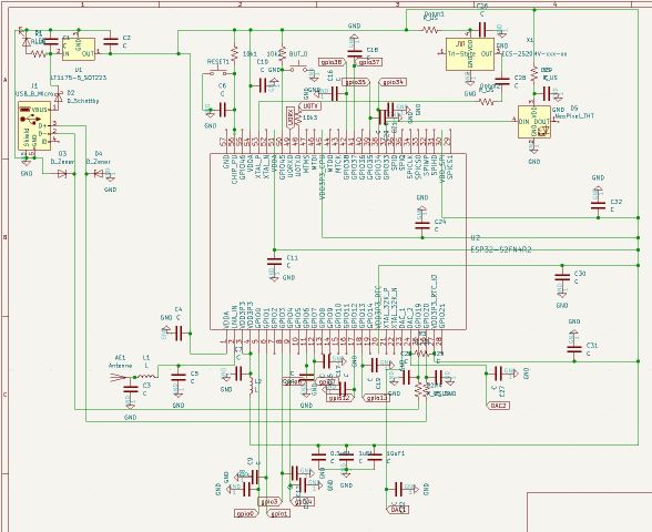
For this week, I wanted to start creating a base board design for my final project. The idea is that this would be a dev-board containing the ESP32-S2FN4R2, which is the chip I decided on for the Song Sonic. I can then add anything extra onto the original design to make it more optimized for other projects, including the Song Sonic. While ambitious, I wanted to practice a bottom-up approach to designing a board to fully understand the fundamentals of each component being used. I think in the end this gave me a great insight on the different blocks of a circuit, which led me to research more into the purpose of individual circuit components such as zener diodes, voltage regulators and crystal oscillators. While familiar with their use cases before hand, I was not sure on how they were implemented into different schematics.
| Design File Links |
|
|---|---|
| - ESP32s2 Dev Board KiCad Schematic |
|
| - ESP32s2 Dev Board Gerber File |
|
| - ESP32s2 Breakout Board with Antenna |
|
Inspiration
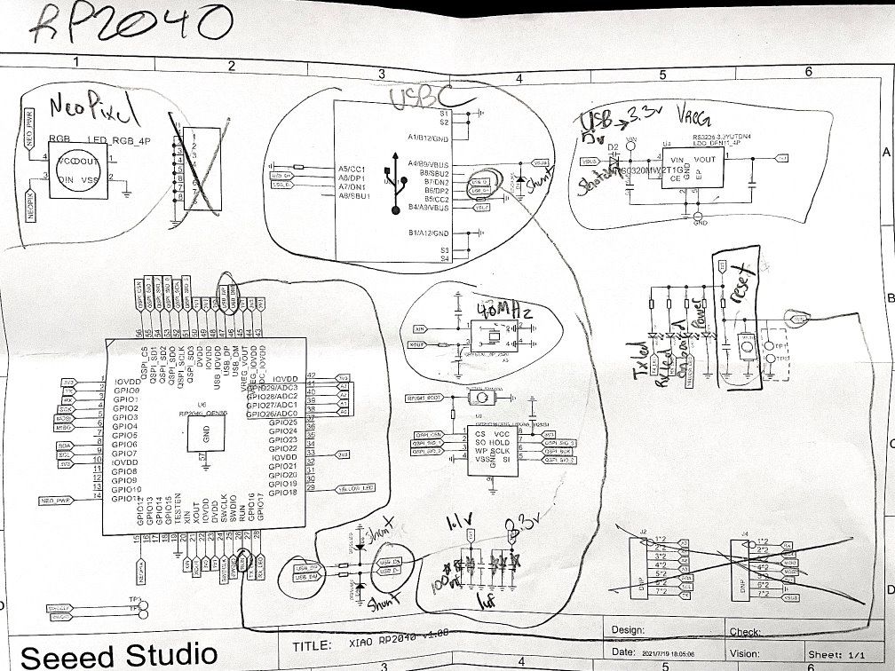
I decided to look at the schematic for the Xiao RP2040 to see what it included. I printed out the schematic, and analyzed it. I circled each part I wanted to incorporate into my board, and noted the important components such as capacitors, resistors, oscillator and the voltage regulator. I also left little notes next to different parts such as the schottky diode, so I can remember the purpose of the component or what the component is.
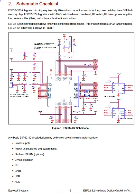
The next step was to look at the required components for the ESP32-s2. I found a link to the ESP32-S2 hardware design guidelines, which has everything you need to design a circuit.
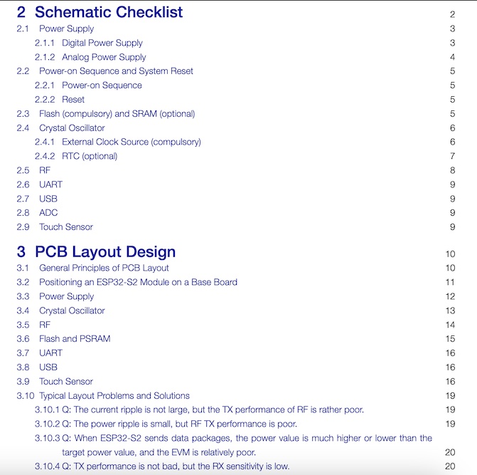
The most important features the guidelines contain is the schematic checklist, and the design rules for how to build each section of the circuit.
The checklist is broken up into the functional parts of the circuit, thereby encapsulating them into their own self-contained systems.
I wanted to figure out what I could keep, and what I could remove from the checklist. In the design rules, it notes whether or not the section of the circuit is compulsory or not needed.
For my circuit I decided to create the following blocks, either due to being required, or because I wanted the feature:
|
|
|
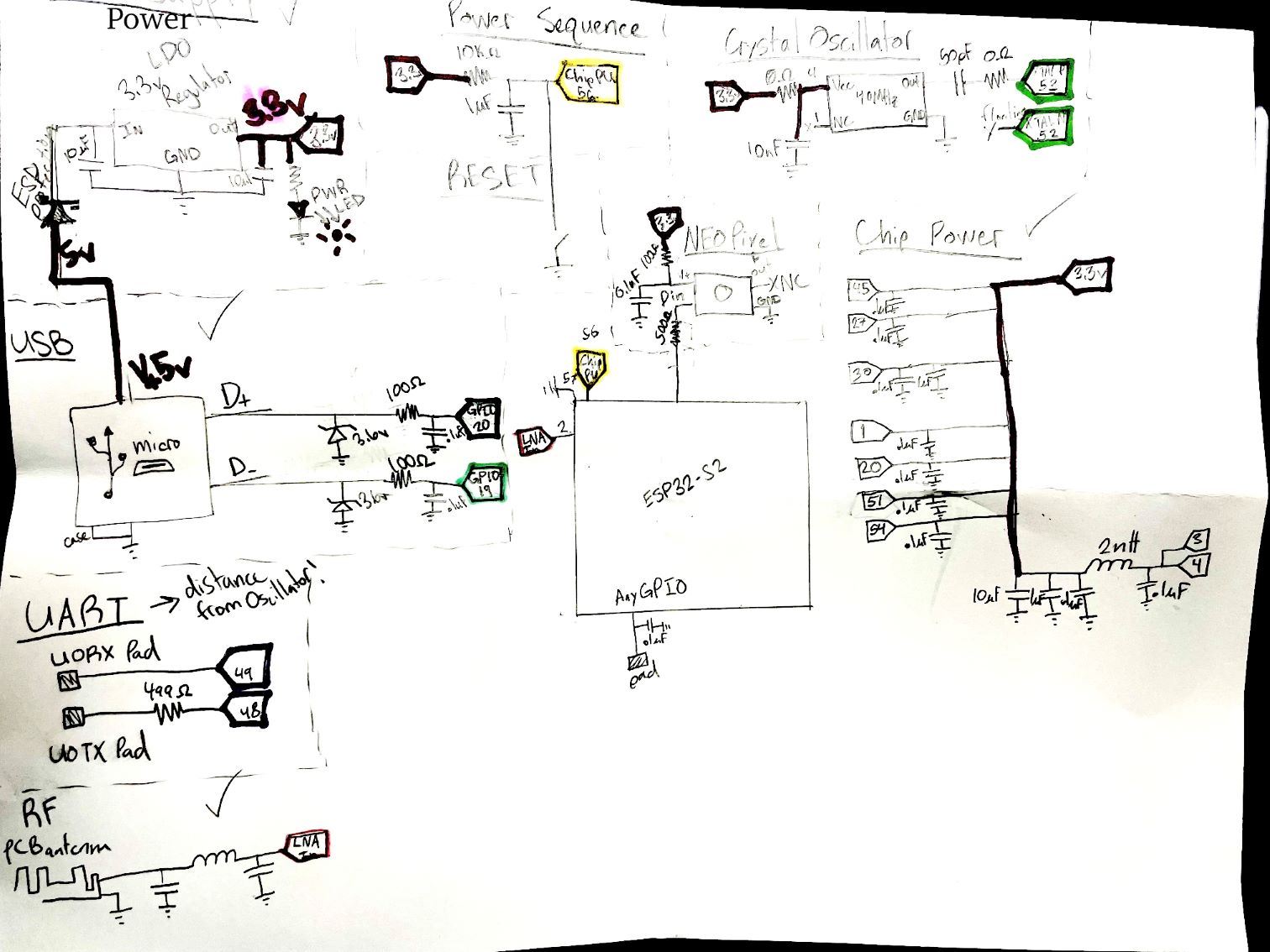
Using this schematic checklist, and the PCB Layout, I started on drafting my own idea for the circuit on paper.
I wanted to make sure I had all the minimal requirements such as the LDO, and crystal, but I also made dedicated sections for the portions I wanted to add like the usb.
Luckily the hardware design guidelines also included a recommendation for the usb circuit, which only required a shottky and 2 zener diodes.
I added a power indicator LED as well, that lights up when it is plugged into power via the usb.
You can view my rough schematic below:
|
Designing in KiCad
|
After designing the circuit by hand, I had a good template for creating the circuit through KiCad.
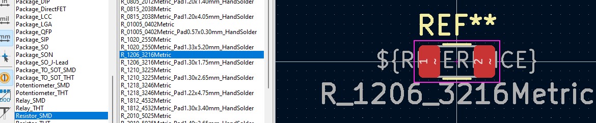
I already have familiarity with KiCad, but to use the esp32s2 on KiCad, I needed to find the KiCad footprint.
It took a bit of searching but I found the footprint/schematic files for the ESP32s2.
You can follow this guide on importing symbols into KiCad's symbol library.
ESP32 Kicad Files - Kicad Schematic Symbol Library - Kicad PCB Footprints Library I found these libraries in the official docs of Espressif. -- Which linked to their github. 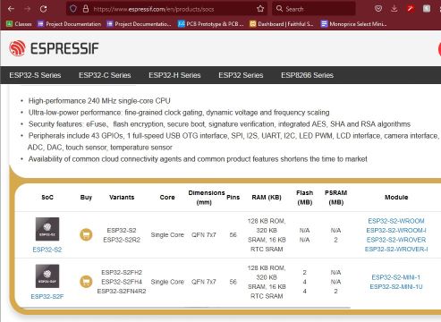
Follow the below instructions if needed to import your symbol and footprint libraries into KiCad 7.0 |
|
Importing Schematic Libraries - In Schematic Editor KiCad 7.0 |
||||||
|---|---|---|---|---|---|---|
Preferences 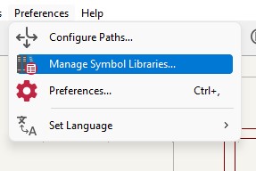
|
|
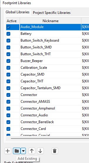
Click Add Existing Library to Table (Folder Icon) 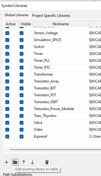
|
|
Locate and select your new Kicad Symbols Library (.kicad_sym) 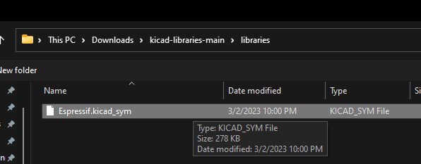
|
|
Confirm adding your new Symbols Library by clicking OK 
|
Similarly, for importing PCB footprints...
|
Importing PCB Footprint Libraries - In PCB Editor KiCad 7.0 |
||||||
|---|---|---|---|---|---|---|
Preferences 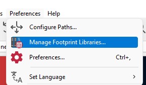
|
|
Click Add Existing (Folder Icon)
|
|
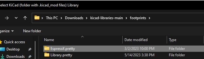
Locate and select your new Kicad Footprints Library Folder (.pretty)
|
|
Confirm adding your new Footprint Library by clicking OK
|
KiCad 7.0 Schematic Editor
| Adding Symbols to Schematics |
|
|---|---|
Start by clicking the Add a symbol Button (looks like an OP AMP) or Press "A" 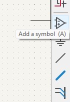
Click anywhere on the schematic, and you will then be greeted by the Choose Symbol window. 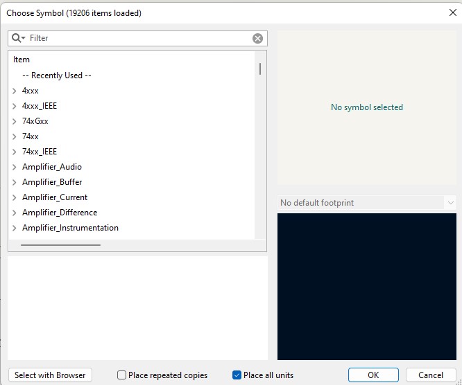
Here, you can search for different symbols, including ones that you imported earlier. 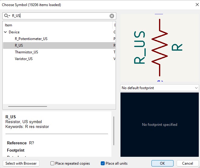 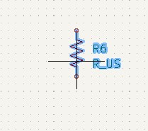
After selecting your desired symbol, you can then confirm it by clicking OK, and then placing it on the schematic by clicking where you want it to go. You can always move it after placing by selecting the same piece and dragging and dropping it. Adding a ground symbol is a similar process, but you will need to select the Add Power Symbol button, which is located below the Add a Symbol button. 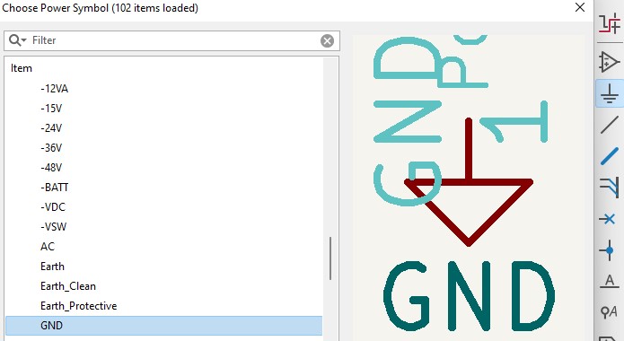
Adding Wires After adding your components, you can use the wire tool (W) to connect each of the nodes of the components according to your design. Here is a quick example of a power indicating LED for a usb input: 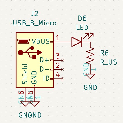
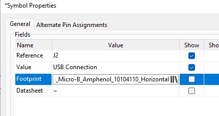
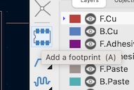
Assigning Footprints After creating your circuit, you are then almost ready to start building the pcb. But first, we need to assign pcb footprints to each component. You can do this by right clicking and editing the properties of a component, then changing the footprint field of the object. 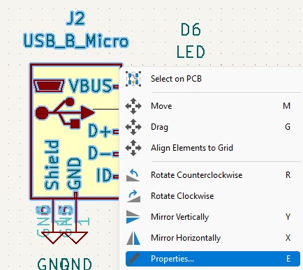
Alternatively, you can verify and change the footprints of multiple objects at once using the footprint assignment tool at the top. 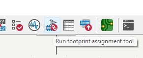 You can then edit and change footprints of each schematic symbol by selecting the footprint in the circled column. 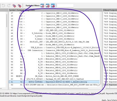
Apply and save, once you have assigned footprints to all of your components. Exporting the Netlist Then export the netlist of components. File 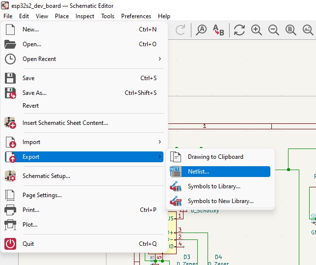
You are now ready to start designing the physical pcb. |
KiCad 7.0 PCB Editor
| Importing Schematic Netlist |
|||
|---|---|---|---|
|
|
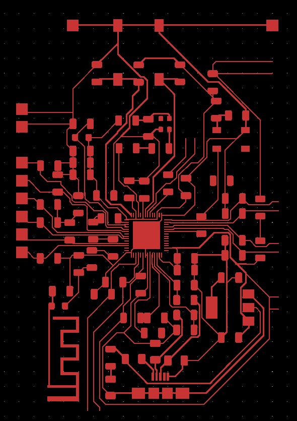
For placing the footprints, I pressed the green PCB editor button while on my schematic file on KiCad.
This populated and placed all my components onto the board, now it was my job to lay them out properly.
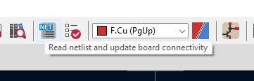
If your board is not populated, you will need to export the netlist as shown above, then import it in the pcb editor.
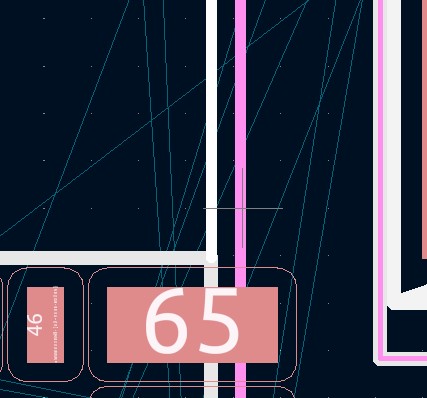
After populating your board with the netlist, you will need to place all of your components on the pcb. They will come in as a group of tightly-packed components, but they will not be in a valid format for making a pcb. You will need to work on laying that out yourself, but in general is is better to give yourself more room to work with than needed, then scale down as you see fit. |
||
| Placing Component Footprints |
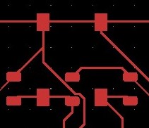
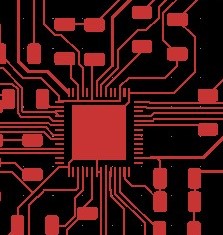
I started by constructing groups of components based on which section of the circuit they belong to, then neatly laying out small circuits around the chip.
I then ordered them around the ESP32s2 chip, and tried to find a layout with the least bit of overlap.
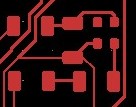
In hindsight, this method, while allows for grouping of related components, ended up producing a fairly messy board. A lot of jumpers ended up getting utilized.
In the Circuit Breakdown section, I go into further detail on the reasoning and design decisions for each section of the board.
Placing a component consists of dragging and dropping them in the desired place. Pressing "R" allows you to rotate the parts orientation. The pcb editor also shows these helpful (blue) lines to show what pad should be connected to another - so it is a good idea to use this as a tool for arranging the components so there are no overlapping lines, then adding wires afterwords.
Below, I explain in detail my placement of components, why I chose them and what they accomplish for my build. |
Circuit Breakdown
In this section, I detail the design reasoning and implementation of the different sections of the circuit.
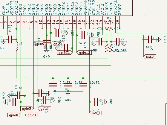
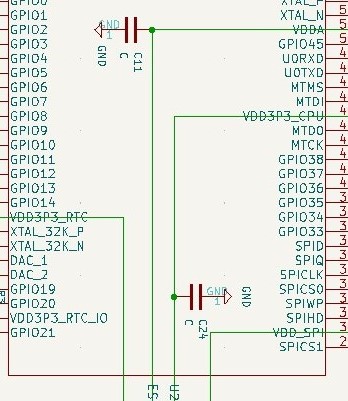
GPIO PinsFor each GPIO pin, that I decided to use, I attached a filtering capacitor to each pin, and ground. This 0.1uF capacitor helps filter signal any noise or rises in current that could occur on each pin. It also acts as a pull-down to ground for a default pin state. Some pins, such as the DAC, required a pull-up resistor in addition. To figure out if a pin needed a pull-up resistor, I looked in the technical design documentation where it lists each pin that requires one. |
Drawing → Schematic → PCB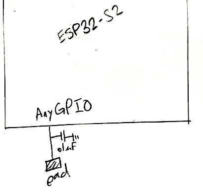

|
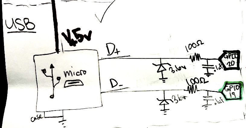
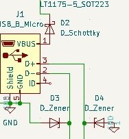
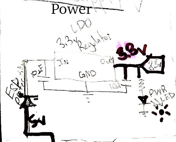
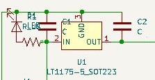
USB and PowerThe usb port has 4 notable connections: power, ground, data+ and data-. The power bus passes through a schottky diode and into the LDO voltage regulator, as well as a power indicating led with accompanying current-limiting resistor. When the usb is plugged in, it should provide 5v to the LDO, which outputs the 3.3v to be used on the ESP32s2's power inputs. A zener diode is connected reverse-biased to the data+ and ground, as well as another connected to data- and ground. These zener diodes help keep the data line at a voltage of approximately 3.3v max, to prevent any damage to the USB port and the chip as well. The zener diodes will sync any excess current directly to ground, once the voltage reaches a certain threshold of 3.3v. The LDO is accompanied by capacitors on the input and output pins. These capacitors act as small power supplies to provide extra charge when the circuit requires it. This results in a smoother output power signal that the chip can rely on. |

|
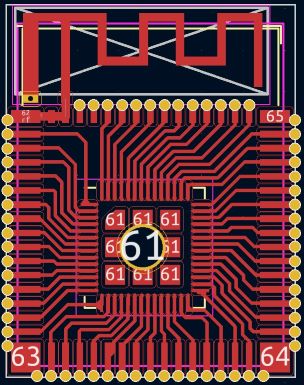
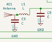
RF AntennaThe antenna for wifi and other wireless protocols is interesting because it gets directly milled into the pcb. Typically you can see boards such as the WEMOS D1 mini, which incorporates a similar pcb antenna integrated right into the board. I am not sure on the RF interactions and whether or not the area around the antenna should be milled away. This will need testing in the future. It is accompanied by an LC filter to act as a band-pass to remove unwanted high and low frequencies. |

|
Neopixel LED -- WARNING LED ORIENTED WRONG: NEEDS UPDATEWhile I accidentally used the wrong LED pinout for this wiring (Doesn't match the ones we have in our lab), the base concepts for the design remain in tact. It has a current limiting resistor connected to power, and a power-smoothing capacitor. Data in goes straight to one of the unused pins of the ESP32 via a 500 ohm resistor. |
|
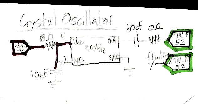
40MHz Cystal OscillatorThe ESP32s2 requires at least a 40MHz clock signal to run. I am using a 40MHz crystal oscillator accompanied by two capacitors to do this. The capacitors are responsible for resonating the oscillator to produce the clock signal. |
|
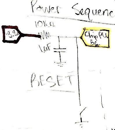
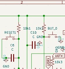
Buttons and Power-On SequenceI have included 2 buttons on this design. One acts as the reset button, and the other as multipurpose GPIO input. With the reset button, I have a capacitor connecting the reset pin to ground. This acts as a quick short while the capacitor is charging up to reset the ESP32s2 on power-up. The other button is connected between a GPIO pin and ground, with a pull-up resistor for a high default state. |
|
Power DistributionThe 3.3v output from the LDO gets fed into various Vdd pins on the ESP32s2. Each pin that requires the 3.3v power is accompanied by a capacitor to help with supplying extra charge for power-smoothing. |
|
Summary of Process and Results
Overall, the process of designing a circuit can be simple but time-consuming (depending on the scale). It is good to always start with a reference circuit, then tailor it to your needs by adding on and removing parts of it. By using the design documentation for the ESP32s2, I was able to design this circuit without having to guess what connects to each pin. While this circuit is not perfect, it helped me gain more familiarity with the actual design of full-fledged dev boards, and I hope to improve this design in the future.
Summary:- Step 1: Find a reference, and draft ideas based on it
- Step 2: Check the design documentation on how to implement each idea and draw a rough draft of the schematic on paper.
- Step 3: Once you have verified your design with the design doc, build the schematic on the computer with an app such as KiCad.
- Step 4: Draw your pcb using the schematic made in step 3.
- Step 5: Repeat steps 1-4 until satisfied with final result