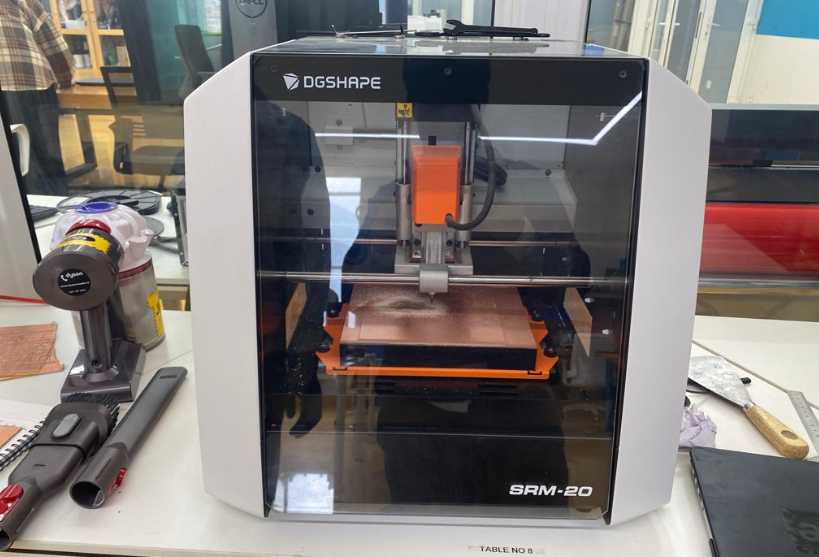
Electronic Production
Eight week of the FabAcademy 2023 was about electronic production and we are required to cut and produce a PCB board and also program that was designed on sixth week. As usual we had group work and individual assignment. However, this week we commenced the session with brief questions and answers on Electronics from which Mr.Rico recommended us to watch YouTube videos on basic electronics and also answer the questions that he has provided in the group chat.
What is circuit?
An electronic circuit is composed of individual electronic components, such as resistors, transistors, capacitors, inductors and diodes, connected by conductive wires or traces through which electric current can flow.
What are different power sources?
The different power sources include Hydropower, Bio fuels, Biomass, wind, geothermal, and Solar
What is load?
An electrical load is simply any component of a circuit that consumes power or energy. In a household setting, the most obvious examples of electrical loads include light bulbs and appliances.
What is conductor?
In physics and electrical engineering, a conductor is an object or type of material that allows the flow of charge in one or more directions. Materials made of metal are common electrical conductors
What is the difference between Voltage, Current and Resistance?
Voltage is the difference in charge between two points. Current is the rate at which charge is flowing. Resistance is a material's tendency to resist the flow of charge (current)
What is the Ohm's law?
Ohm's law states that the voltage across a conductor is directly proportional to the current flowing through it, provided all physical conditions and temperatures remain constant. V=IR
What does resistor do?
A resistor is an electrical component that limits or regulates the flow of electrical current in an electronic circuit. Resistors can also be used to provide a specific voltage for an active device such as a transistor.
What does capacitor do?
Unlike the battery, a capacitor is a circuit component that temporarily stores electrical energy through distributing charged particles on (generally two) plates to create a potential difference. A capacitor can take a shorter time than a battery to charge up and it can release all the energy very quickly.
What does diode do?
A diode is a semiconductor device that essentially acts as a one-way switch for current. It allows current to flow easily in one direction, but severely restricts current from flowing in the opposite direction.
What does LED mean?
Light Emitting Diode
What is regulator?
A voltage regulator is a circuit that creates and maintains a fixed output voltage, irrespective of changes to the input voltage or load conditions. Voltage regulators (VRs) keep the voltages from a power supply within a range that is compatible with the other electrical components.
What is bypass capacitor?
A bypass capacitor is a capacitor that is placed between a direct current signal and ground to remove any alternating current component of the signal by creating an alternating current short circuit to ground. The bypass capacitor is used to bypass the power supply or other high-impedance component of a circuit.
What is a Current Limiting Resistor for an LED do?
The current limiting resistor limits the current for the LED and regulates the difference in voltage drops between the LED and the power supply.
How are Capacitors used as High-pass and Low-pass filters? What does it filter?
Filters are electronic circuits that eliminate a portion of an AC signal. A capacitor filter is one type of filters. A low pass filter allows signals lower than a cut-off frequency to pass, whereas a high pass filter allows signals higher than a cut-off frequency to pass.
What is VCC? What is GND? What is Common Ground?
VCC-Common Collector Voltage(VCC is the power input of a device. It may be positive or negative with respect to GND, but most of the world runs on positive voltages like in a vehicle.) GND-Ground(in electronics and electrical engineering, it is by convention we define a point in a circuit as a reference point. This reference point is known as ground (or GND) and carries a voltage of 0V). Common Ground-Electronic devices that don't plug into a wall socket have a different type of ground usually called common ground. A circuit that runs on batteries will often use the battery's negative terminal as common ground - a reference point of zero volts compared to the battery's positive terminal.
What is a Ground Plane and why is it used?
The ground plane on a printed circuit board is a conducting body that acts as an arbitrary node of potential voltage and a common return for electric current. It is a point of zero reference or zero volts. The ground planes in a PCB also serve as the most common return path for the signals on the board. Each signal conducted through a trace has to return to its source, and it will find the path of least resistance.
Group Assignment
Group Members
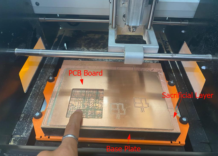
In week 8 (Electronics Production), group work was about characterization of design rules for our Lab (JNWSFL) PCB(Printed Circuit Board) production process. We kick started the session with recitation from Ms.Zina in person and Mr.Rico virtually. Then Ms. Zina briefed us on the purpose of using a sacrificial layer which is to prevent the base plate from any damage in case the Z-position of an end mill is not set properly. Also, their instruction on inserting and removing end mill from the spindle head along with caution to not over tighten the end mill (which would lead to slipping of threads of end mill holder) was well received by participants. We were also informed about the requirement of changing the sacrificial layer timely to avoid uneven laying of PCB on the bed before the milling process.The link to group assignment is Bhutan FAB23 group
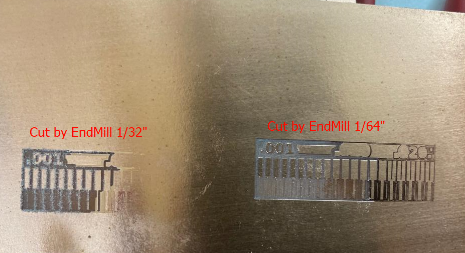
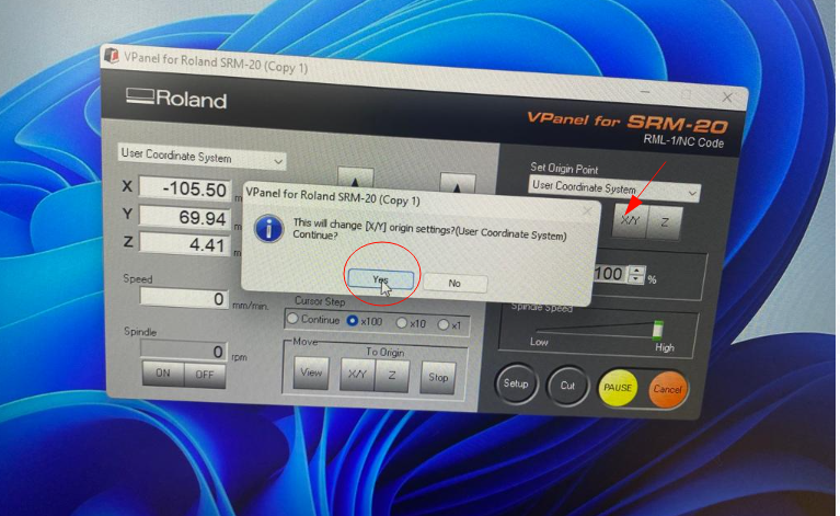
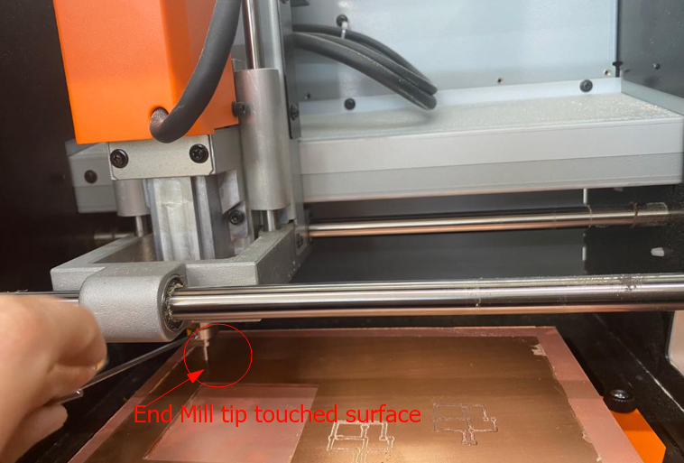
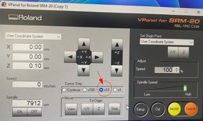
We learned about using SRM 20 to mill the PCB board, changing the end mills, and setting XY & Z position of an end mill from VPpanel in the computer. When cutting traces with end mills 1/64" and 1/32" we found some differences and they are:
Individual Assignment
Individually, we were supposed to cut and produce the PCB board using SRM20(milling machine) and mods that we have already designed in KiCAD. And the work flow of assignment as described below:
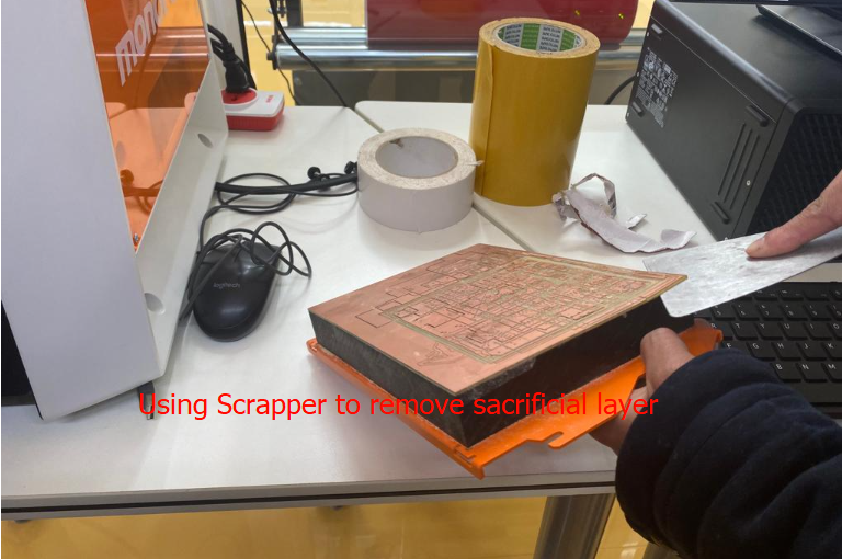
Changing Sacrificial Layer
While changing the sacrificial layer, we removed the base plate on which the sacrificial layer is attached. After removing the base plate we removed the sacrificial layer with the help of scraper and cleaned the leftover of double sided tape (which is used to attach base plate and sacrificial layer) with the help of colin and napkin cloth. Then fixed back the base plate.

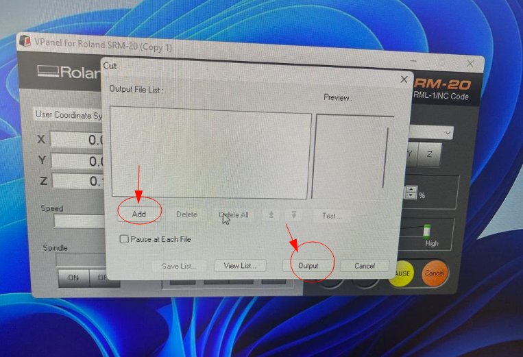
Using mods to convert the PNG to rml file
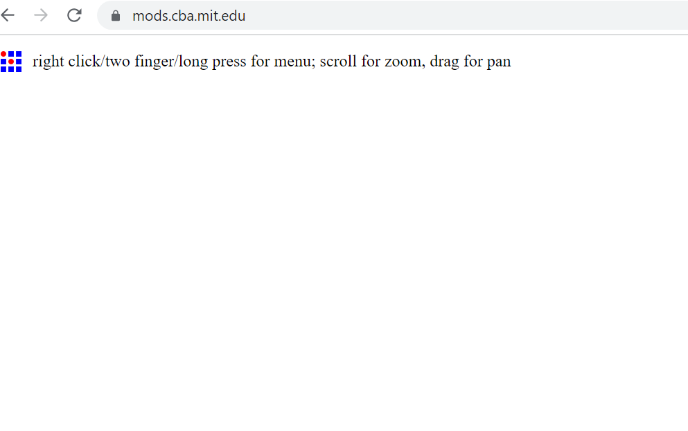
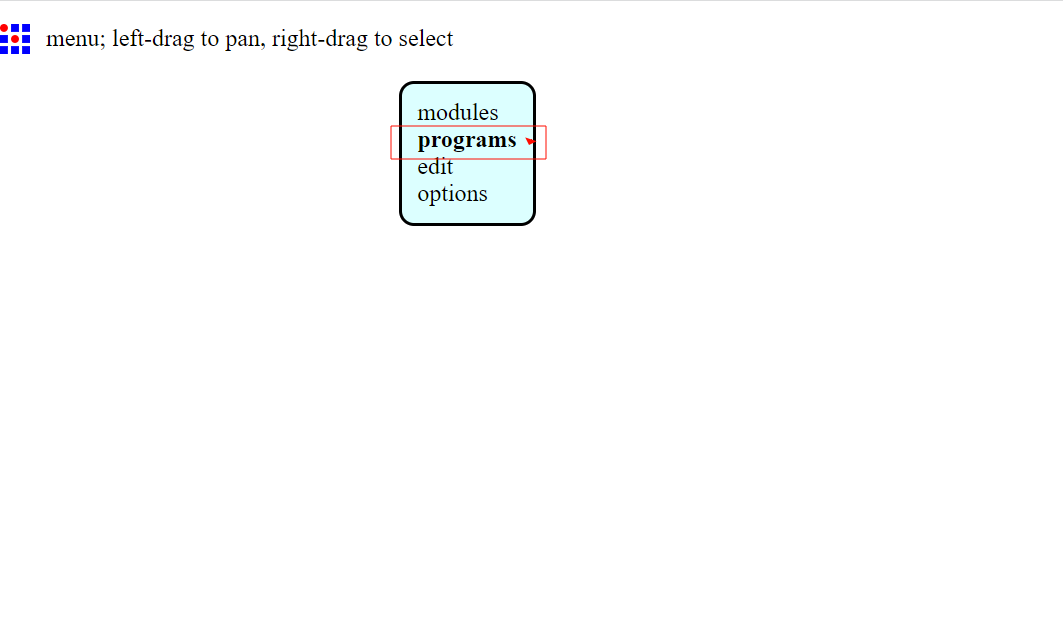
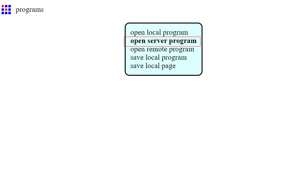
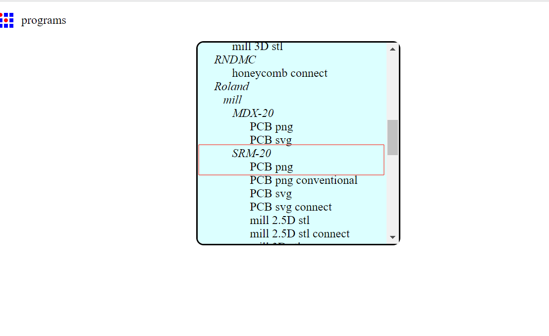
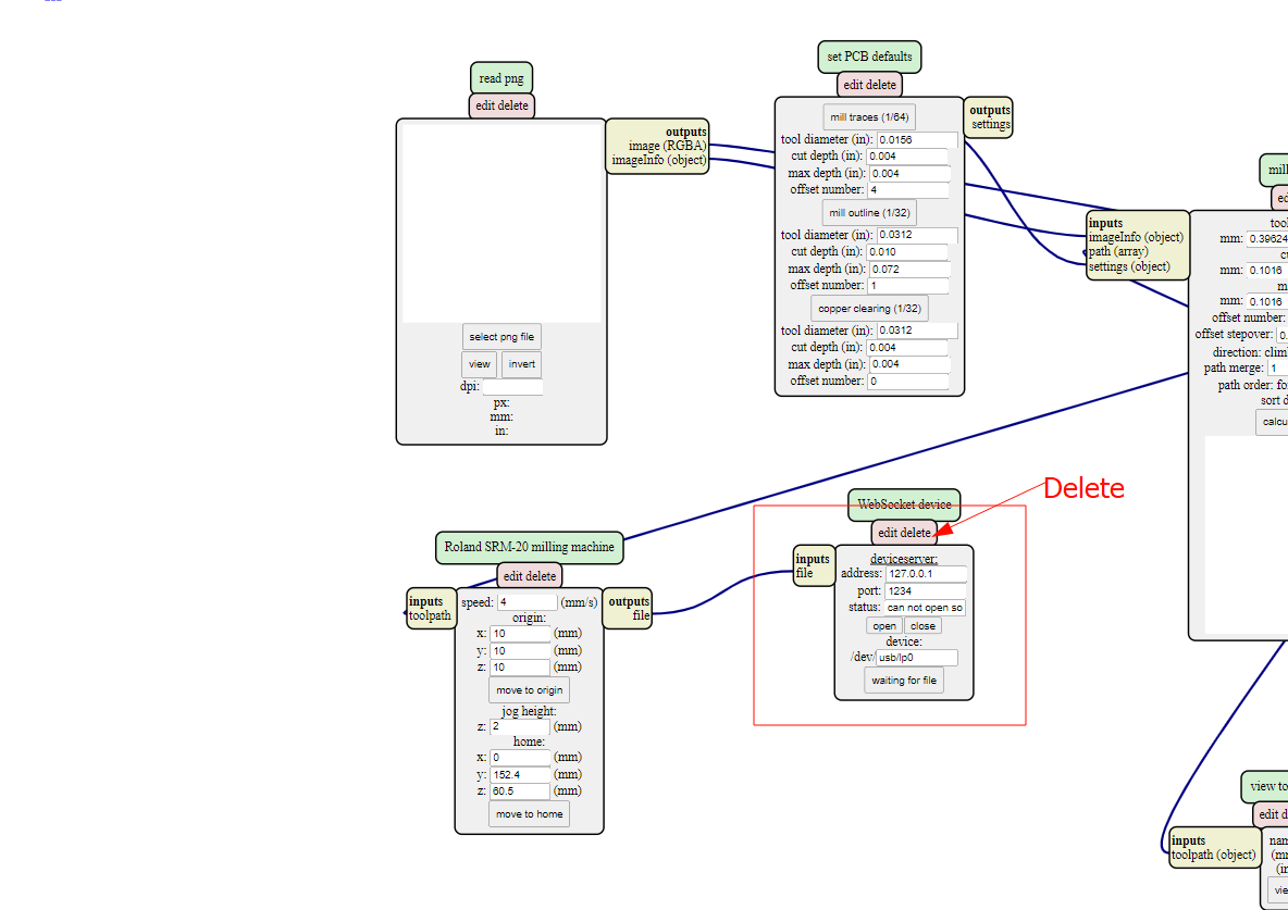
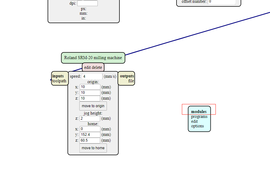
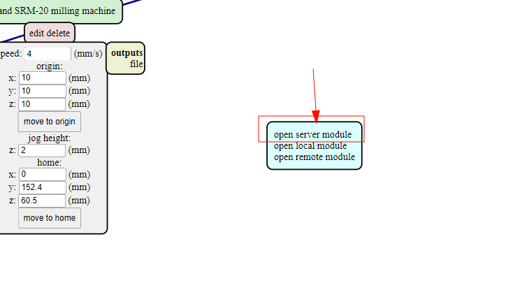
We logged into the mods.cba.mit.edu from google chrome where we were directed to the mods site >> On that site you right click and select programs >> then select open server program >> Scroll down and click on PCB png under SRM20.
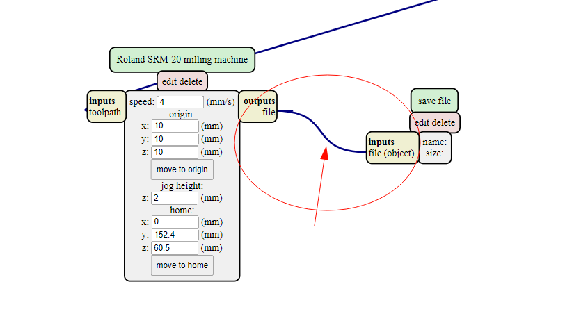
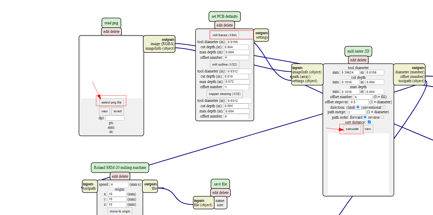
Setting XY and Z positions on Computer
Updating Schematic and PCB board
I had trouble with schematic and PCB routing. Although, you do not get electrical errors and errors on design rules checker alike, but when you route you have to be very careful. I routed following the possible line connection shown by the PCB editor board but it failed several times. I spent four days milling, redoing schematic diagram and editing PCB. Finally, with help and recommendation from Ms.Yeshey, I could come up with successful schematic and routing that could be programmed without which I could not have completed the board production process. Learn to route accurately as possible. My design files are added at bottom of page for reference.
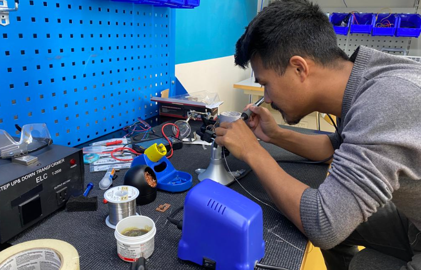
Soldering PCB after milling in SRM20
Soldering was also another arduous task for me. I had basics ideas and skills as well for soldering which I learned during Prefab Academy. However, for this week I had very difficult time trying to choose correct component for my programmable board. I had to be careful when soldering in order to prevent components like LED from getting burned out and moreover, the components were tiny which demanded our precision and patience.
Issues Encountered
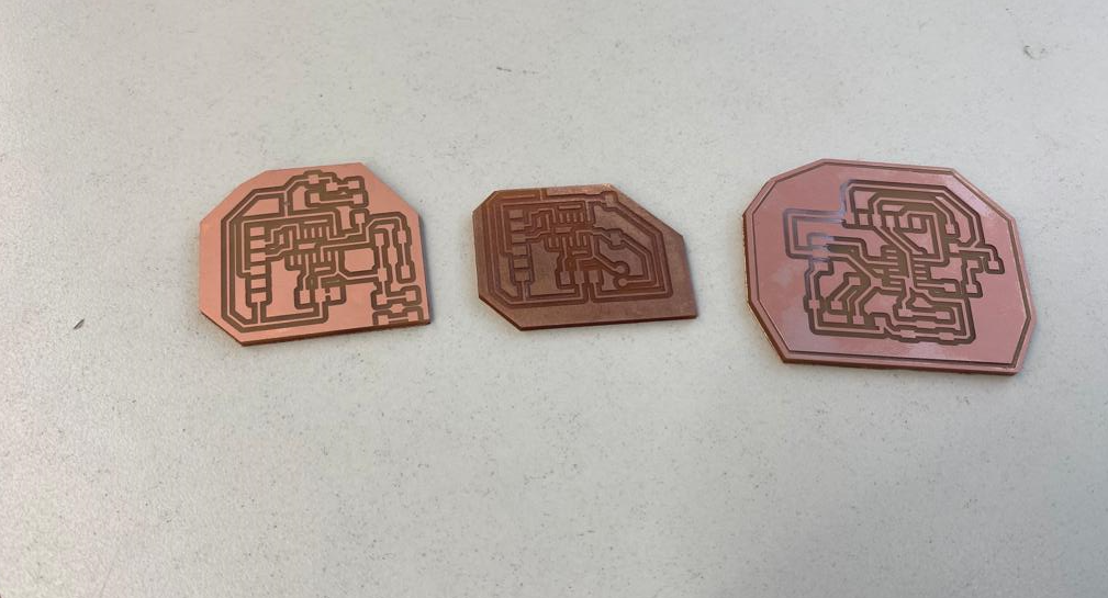
There were several issues in this week, that is to mill a board for several times, checking continuity for footprints and sometime getting short circuited prints despite having no errors from design rules checker. I had milled about 5 to 6 board that malfunctioned, three soldered which didn't work. Finally, I could mill one and solder correctly which worked. To make it successfully, I had to solder, de-solder and cut come connected ends of copper. Moreover, I forgot to check the value of resistor and once I had it soldered with 10MOhm which didn't work and had to resolder it. Mr. Cheche, helped me a lot in reading the values of components because the labeling of the boxes and real components rating were different.
The images below are the failed products
Errors In Schematic
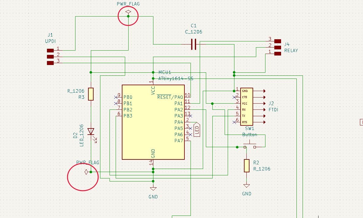
Previously during electronic design week I have successfully designed schematic diagram of PCB board without any electrical error. But during electronic production my schematic and PCB editor didn't work. This is because I had used two power flags in my design. I came to know only after milling the board. The image below shows the error of my schematic design.
After soldering, when I tried to connect to my computer the power LED did not turn on. So I had to recheck my schematic seeking help from Mr.Cheche. The image below is the failed soldered board.
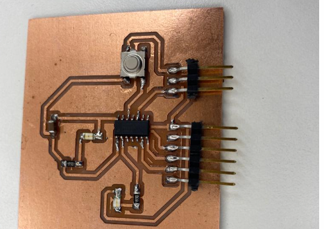
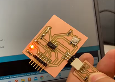
Up on checking my schematic by Mr. Cheche, he found that I have used two power flags in my circuit diagram that affected my final board. Therefore, I removed the power flag and the issues were resolved.The image below is the board that worked.The final design file is attached for reference. Also the hero shot of the week is being able to design, mill and solder the board that worked.
There was another problem with my schematic. I had used different footprints for my resistors and not from the fab library which I was supposed to be using. Therefore I have also changed the footprints of resistor.
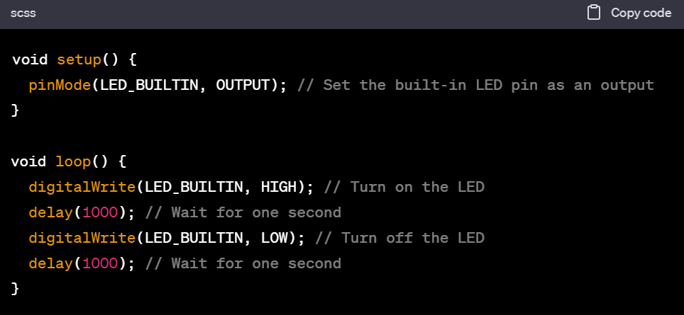
Blink Test
Finally, my board was successful (known by glowing of LED which signals receiving of input power) and then conducted blink test. I had connected my LED to PA4 on MCU(ATtiny1614) which is 0 for coding.
Code for Blink Test
        void setup() {
        // Set the LED pin as an output
        pinMode(0, OUTPUT);
        }

        void loop() {
        // Turn on the LED
        digitalWrite(0, HIGH);
        // Wait for 1 second
        delay(1000);
        // Turn off the LED
        digitalWrite(0, LOW);
        // Wait for 1 second
        delay(1000);
        }
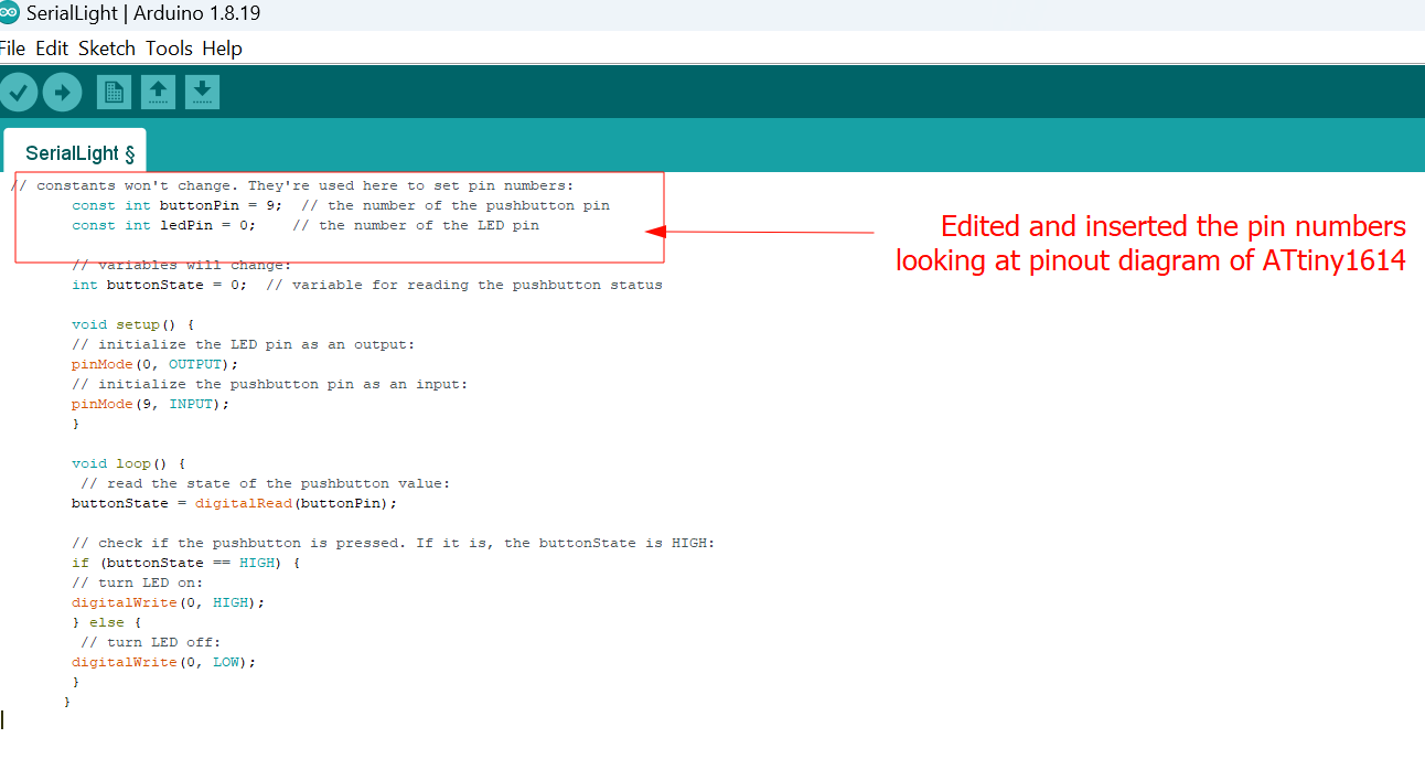
Push Button Test
After blink test, I had to conduct push button test which means controlling the LED with push button that I had installed.
        // constants won't change. They're used here to set pin numbers:
        const int buttonPin = 9;  // the number of the pushbutton pin
        const int ledPin = 0;    // the number of the LED pin

        // variables will change:
        int buttonState = 0;  // variable for reading the pushbutton status

        void setup() {
        // initialize the LED pin as an output:
        pinMode(0, OUTPUT);
        // initialize the pushbutton pin as an input:
        pinMode(9, INPUT);
        }

        void loop() {
         // read the state of the pushbutton value:
        buttonState = digitalRead(buttonPin);

        // check if the pushbutton is pressed. If it is, the buttonState is HIGH:
        if (buttonState == HIGH) {
        // turn LED on:
        digitalWrite(0, HIGH);
        } else {
         // turn LED off:
        digitalWrite(0, LOW);
        }
       }
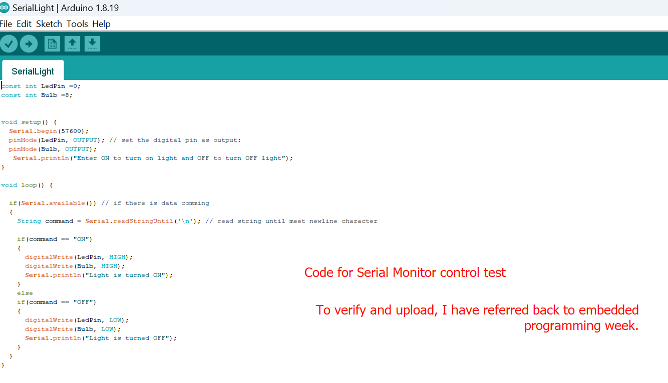
Serial Monitor Test
Finally, I had to test my board to control from serial monitor.
Resources (Programming the Board)
For all the tests I used Arduino IDE to compile and upload the codes. However, I have used the codes from Google or ChatGPT. Most of the time code from ChatGPT appeared to be relative and I had to edit or reconfigure to make it work and therefore, Mr.Cheche advised me to use it from the similar documentation or google which was easier to understand and had some good explanations and link to the codes that I edited are Codes
Arduino Workflows
Whenever I had to compile and upload the codes to program my board, I used Arduino IDE 1.8 and test run to verify if my board was functional and test are such as blink test, push button test and serial monitor control test. Usage of Arduino IDE can be better understood with the images as shown below.
An example of code for blink test from ChatGPT is shown, where you only require to change the pin number and define your constant.
Design File
Schematic and PCB Editor