Electronics Design
Week sixth on electronics design is about a category of software tools for designing electronic systems such as integrated circuits and printed circuit boards (PCB). The tools work together in a design flow that chip designers use to design and analyze entire semiconductor chips.
Group Assignment
Using lab equipment to observe the operation of micro-controller circuit boards. For this week we have been using digital multimeter and oscilloscope (To study the characteristics of voltage-test and display voltage signals as waveforms, visual representations of the variation of voltage over time. The signals are plotted on a graph, which shows how the signal changes). Generally, multimeter is used to test the continuity of connections, measure voltage, amps, resistance etc.
Group Assignment link
FAB Bhutan 2023
Individual Assignment
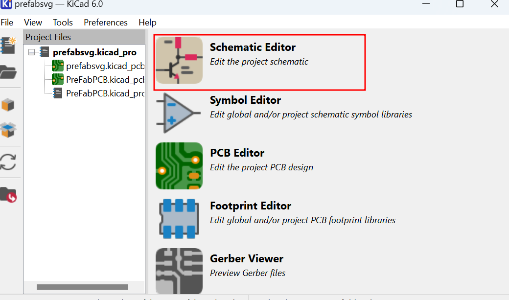
Designing a development board to interact and communicate with an embedded micro-controller. For this we need KiCAD or Eagle and I have KiCAD installed from PreFab Academy session.
Electronic Board Design
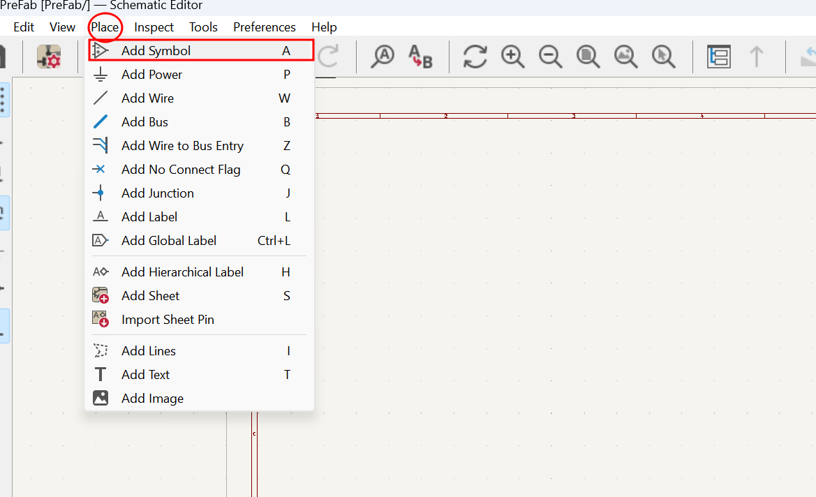
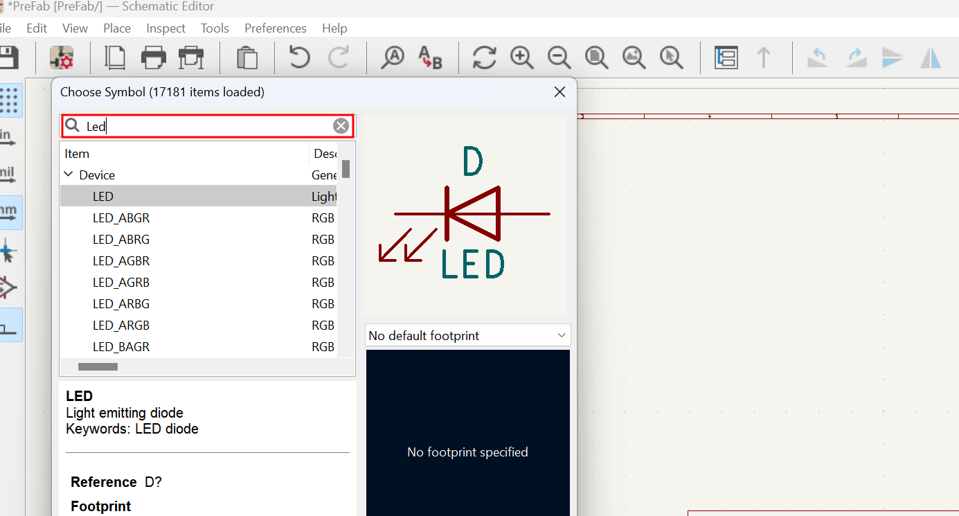
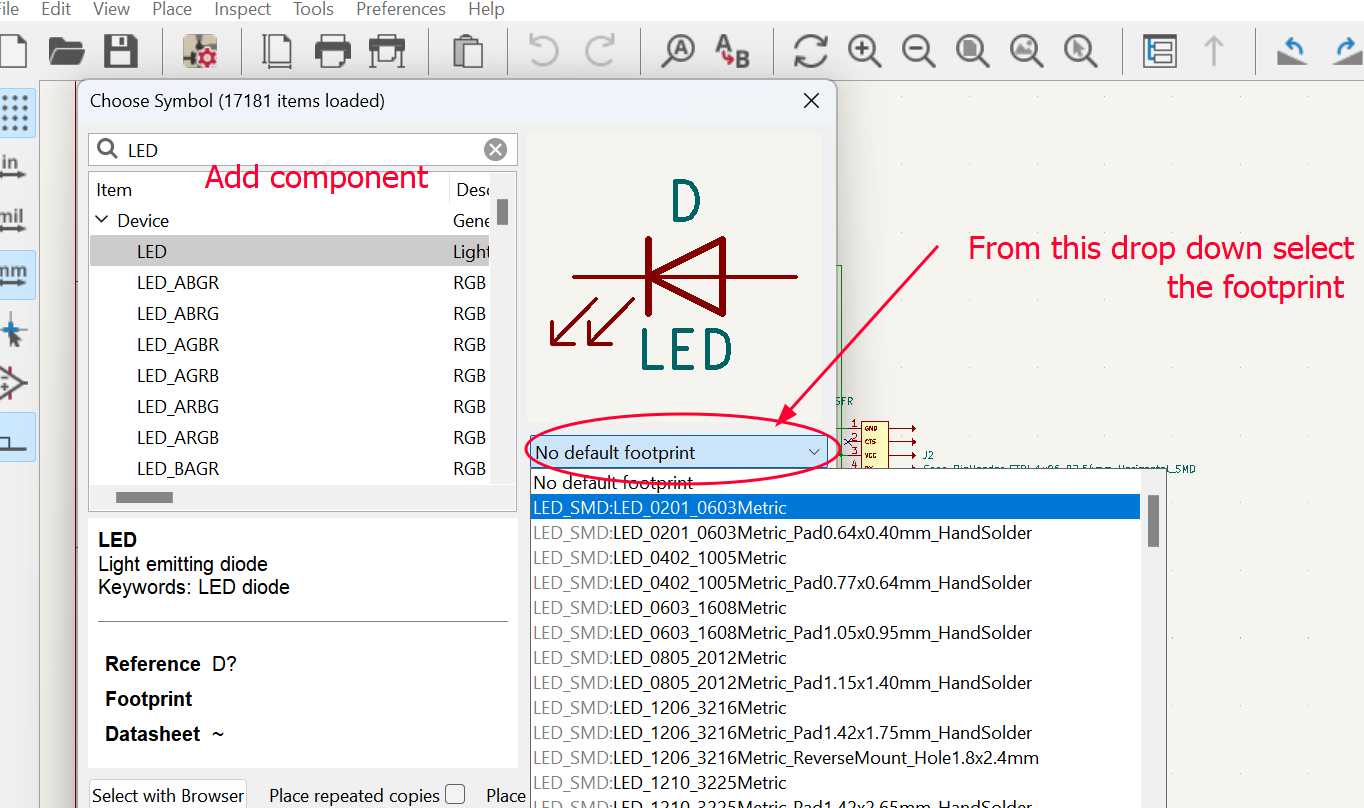
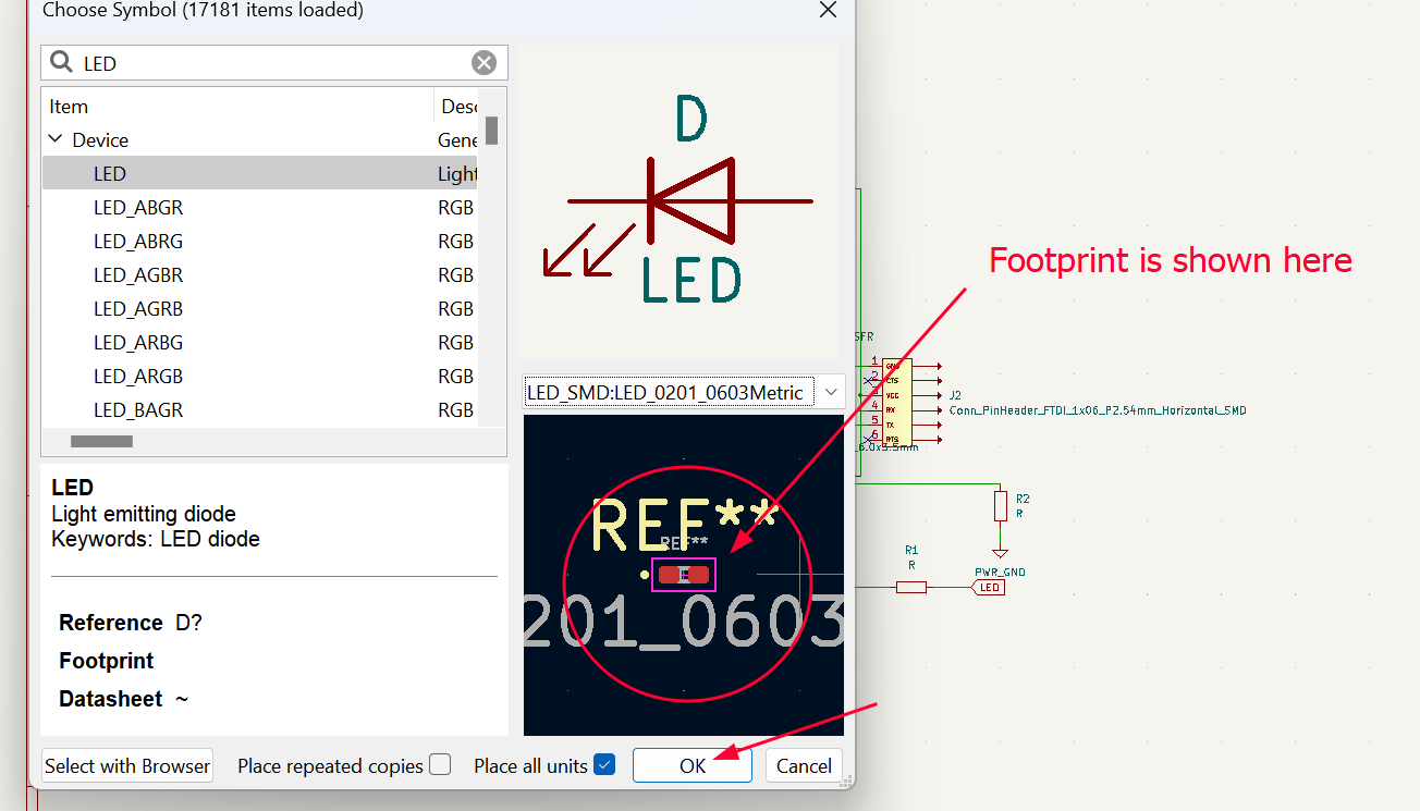
I learned KiCAD and had very little knowledge on using KiCAD. Ms.Zina ran overview on designing electronic board in KiCAD especially the schematic design. KiCAD is important software used in electronic design. Moreover, eagle can be used as electronic design software. To start with schematic design in KiCAD:
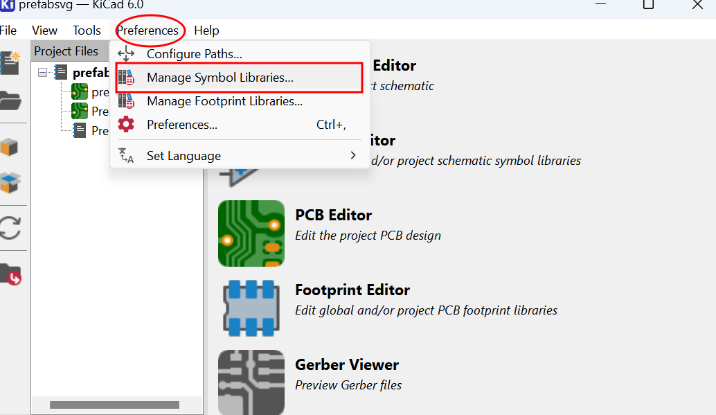
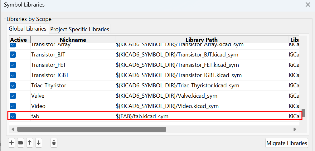
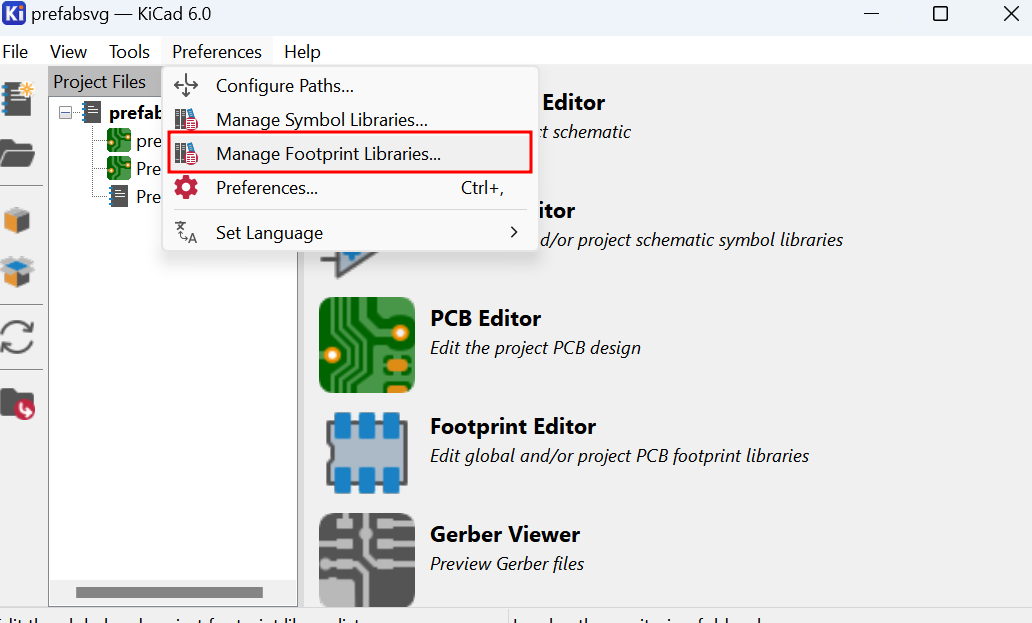
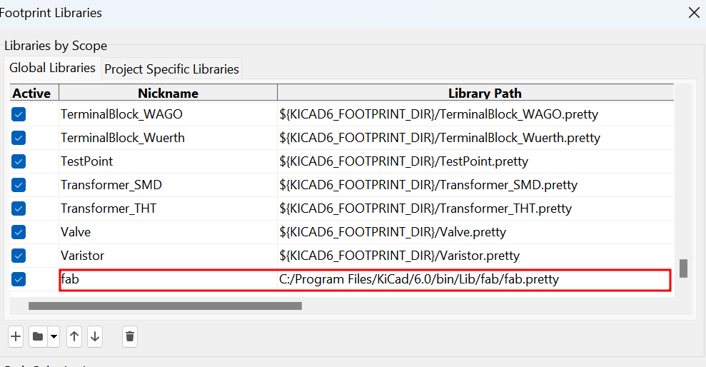
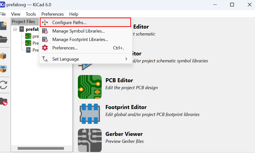
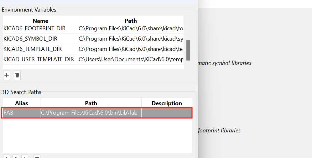
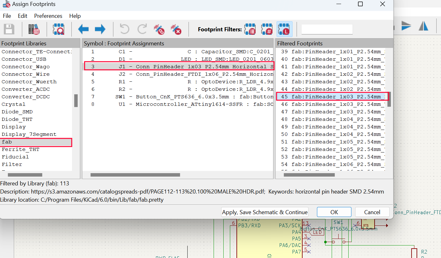
Adding Libraries- FAB Electronic
Before getting into the design, it is important to add libraries of FAB electronic components. To do that need to follow few steps: I followed installation guide from Git Repository and I installed symbol&footprint libraries, and configured the path.
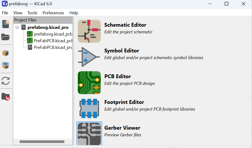
Now you are set to go with schematic and PCB editor in KiCAD 6.0
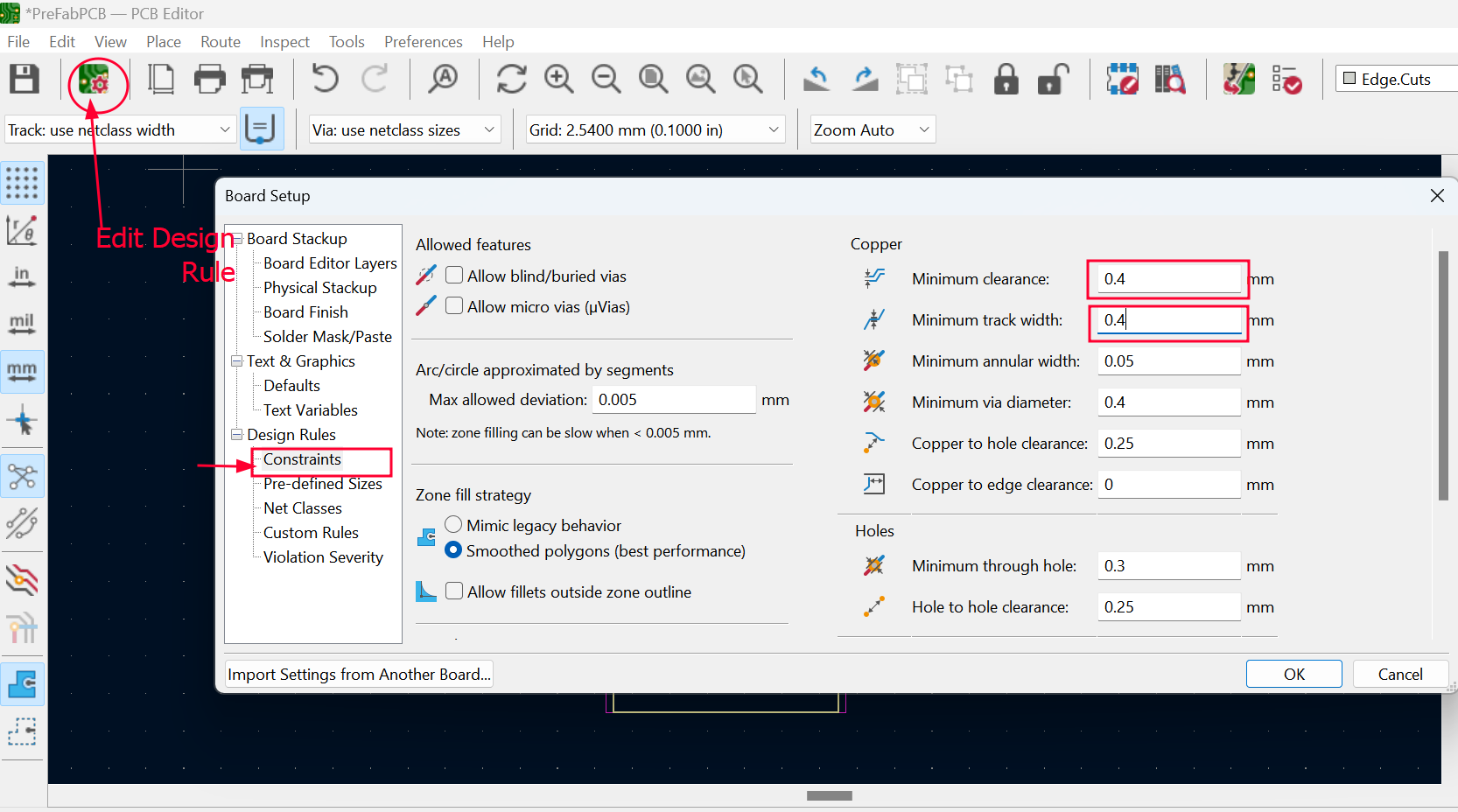
Development Board Designing (PCB-Printed Circuit Board)
Note:This is the end of Schematic Editor and now go with PCB Editor
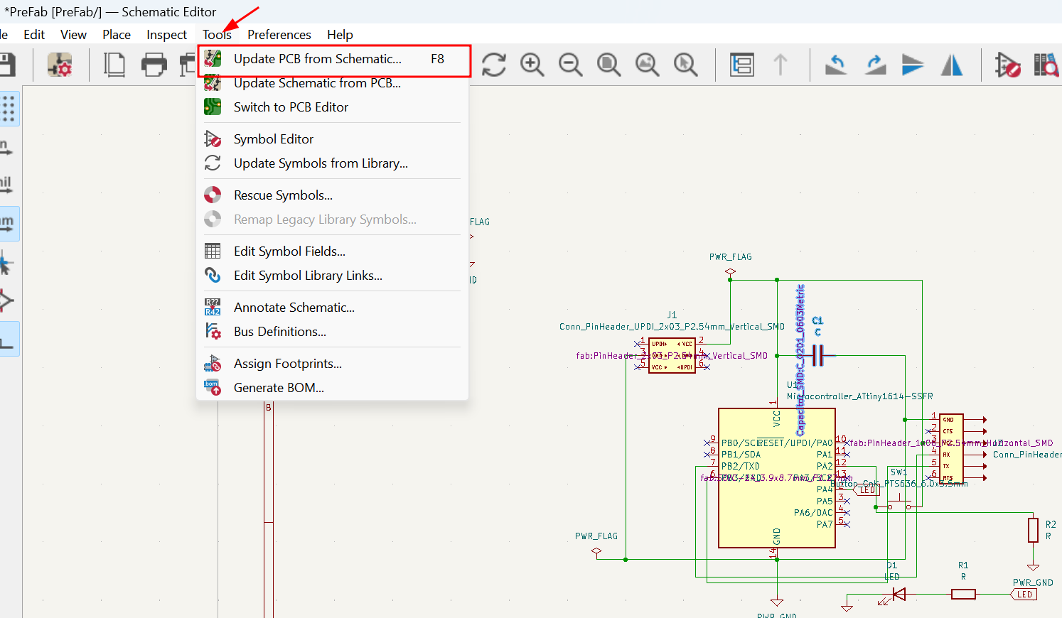
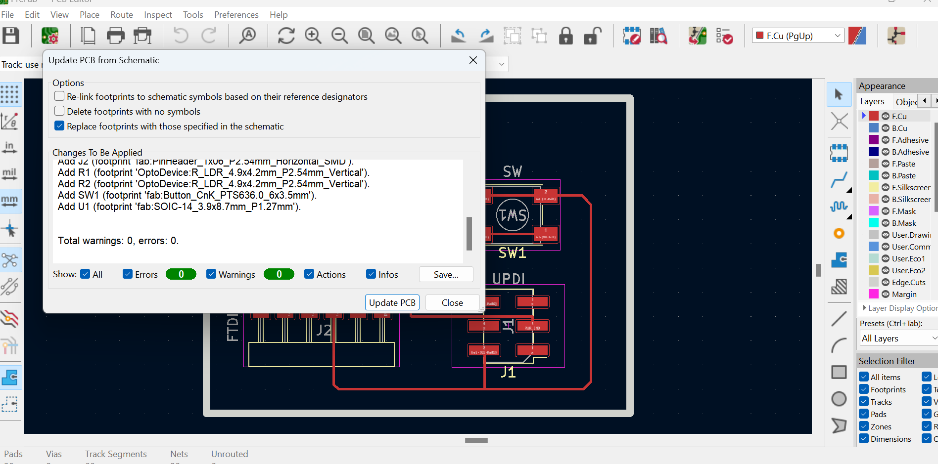
Updating Schematic to PCB Editor
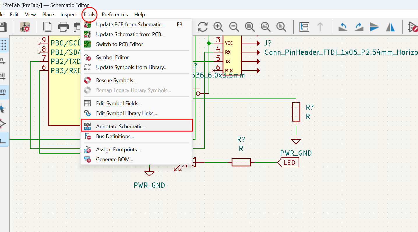
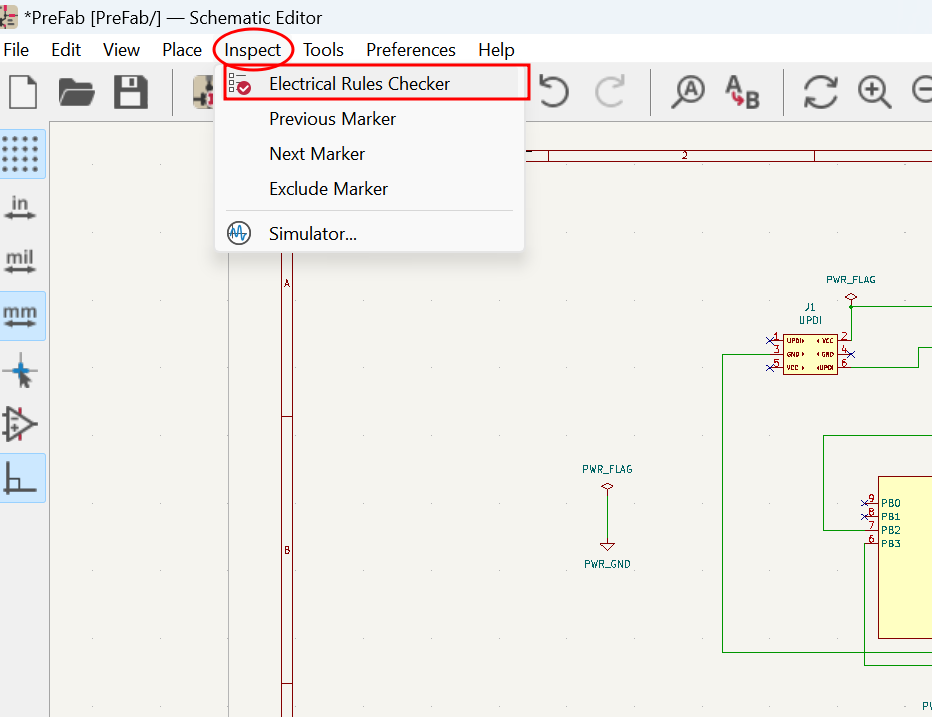
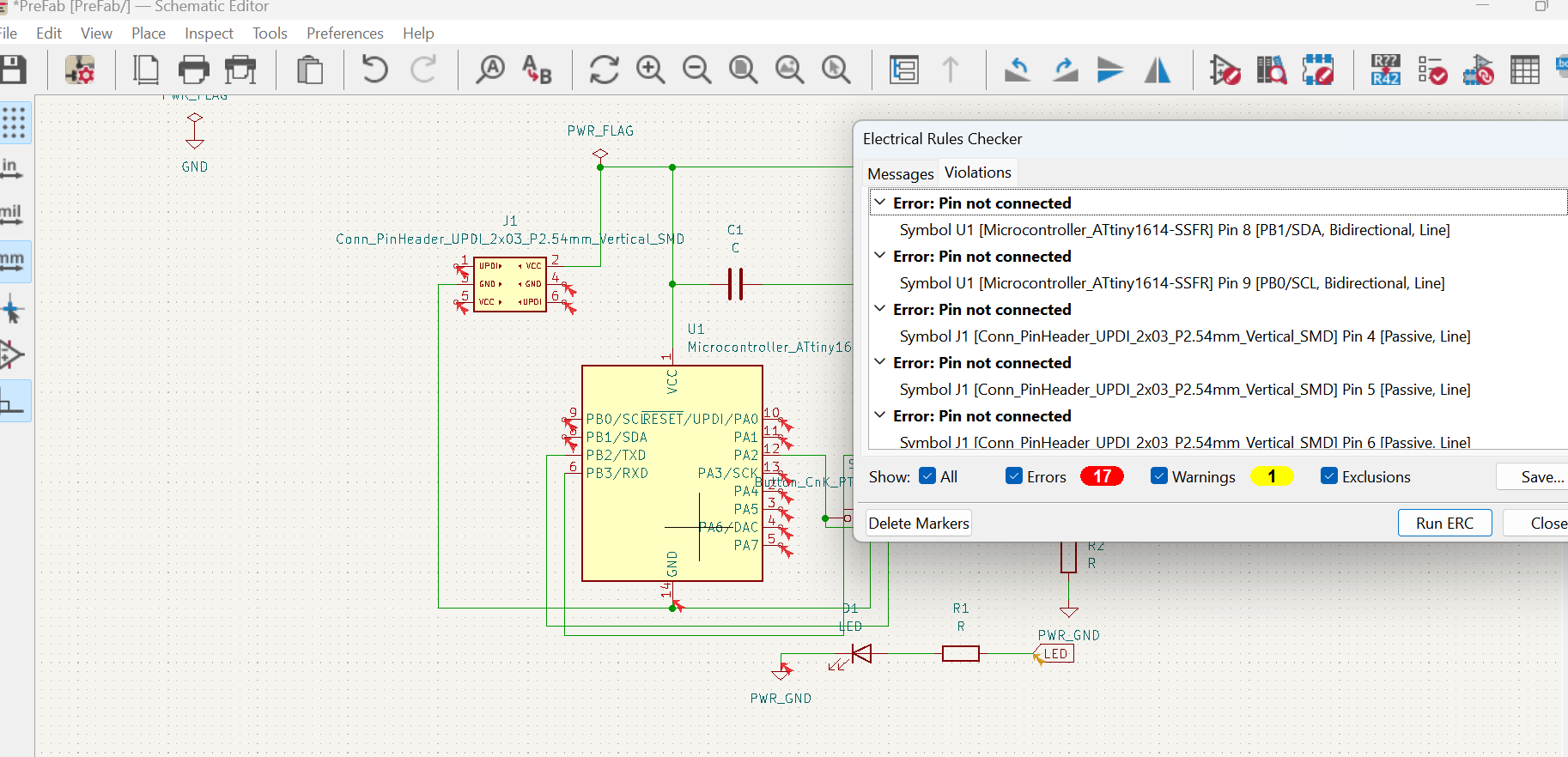
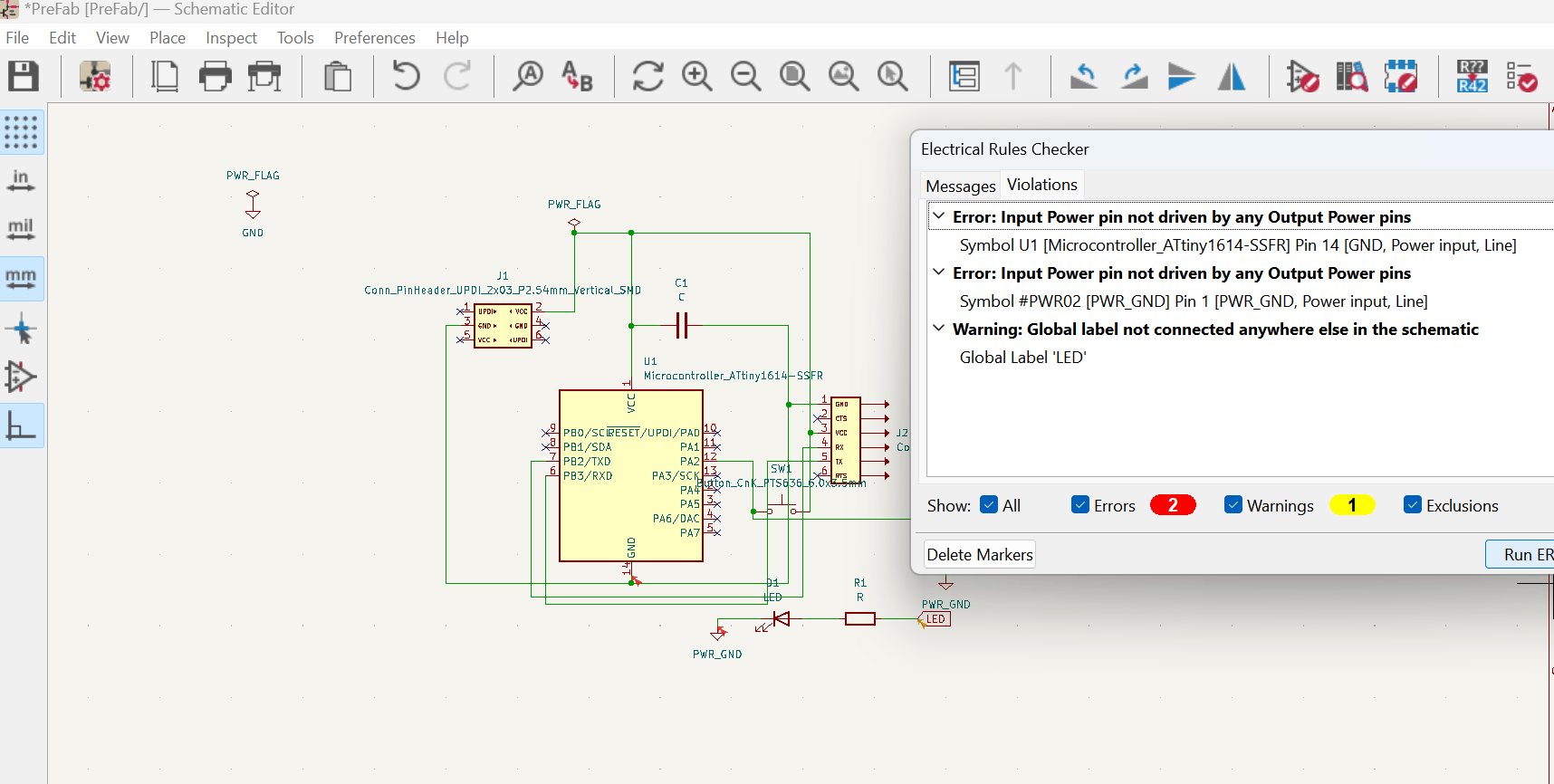
Now I need to update PCB from Schematic and to do that some of the steps are as shown:
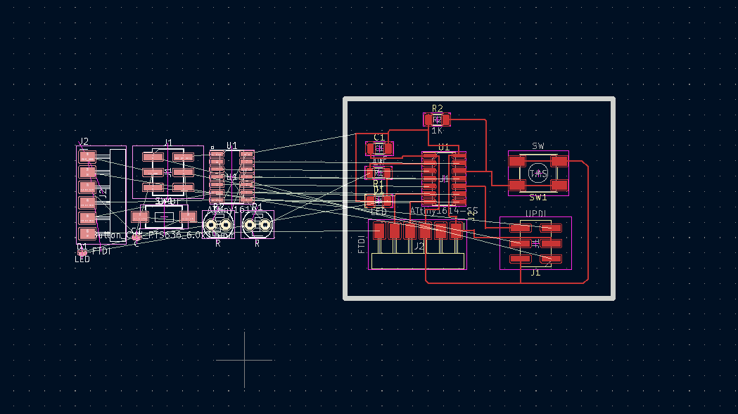
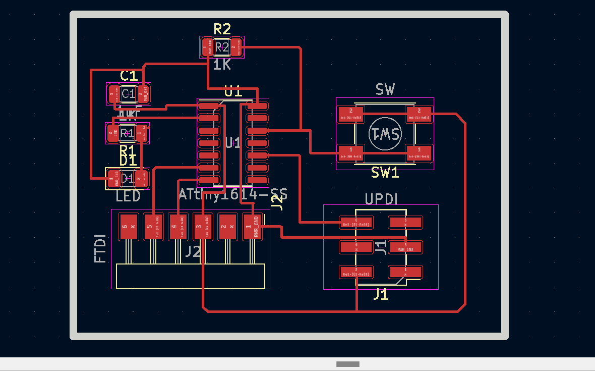
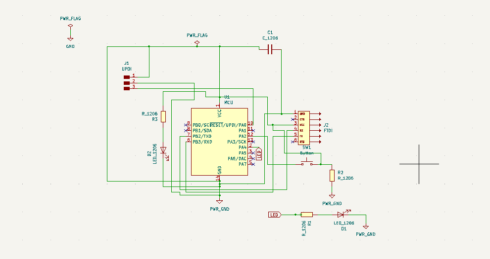
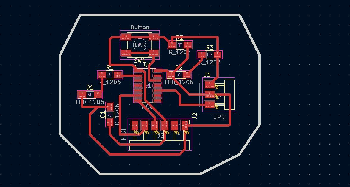
Updated Schematic and PCB
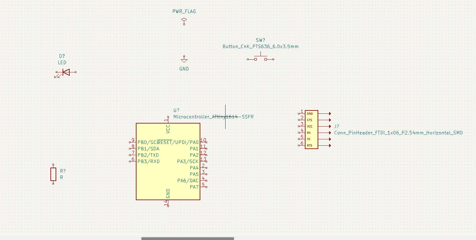
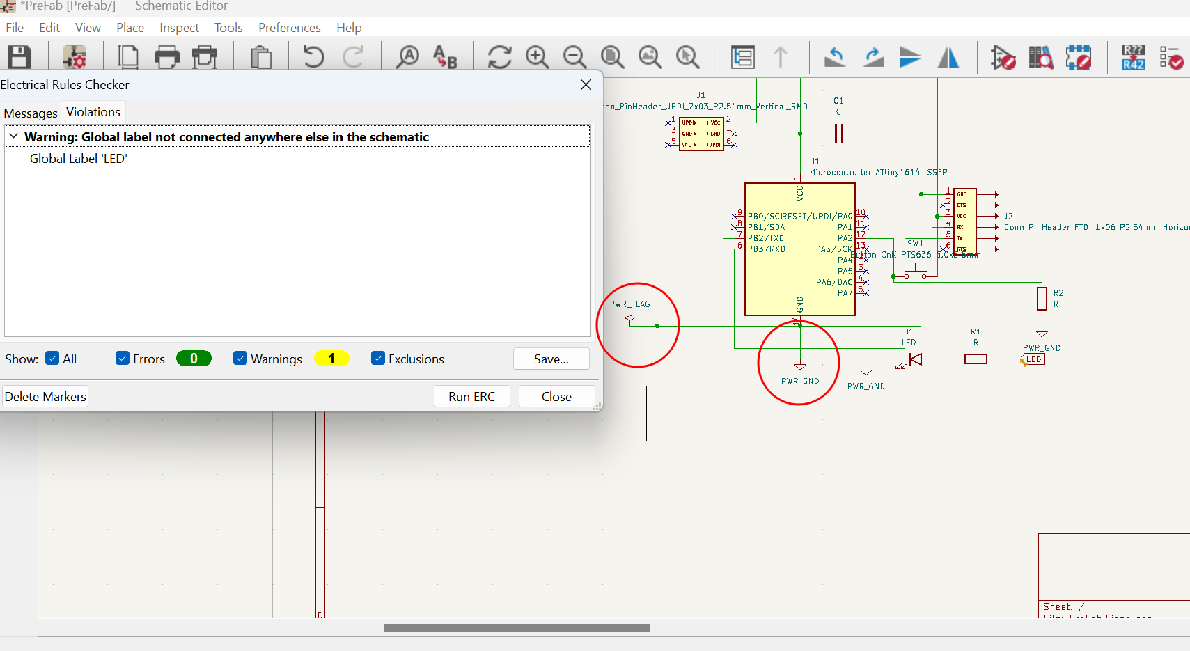
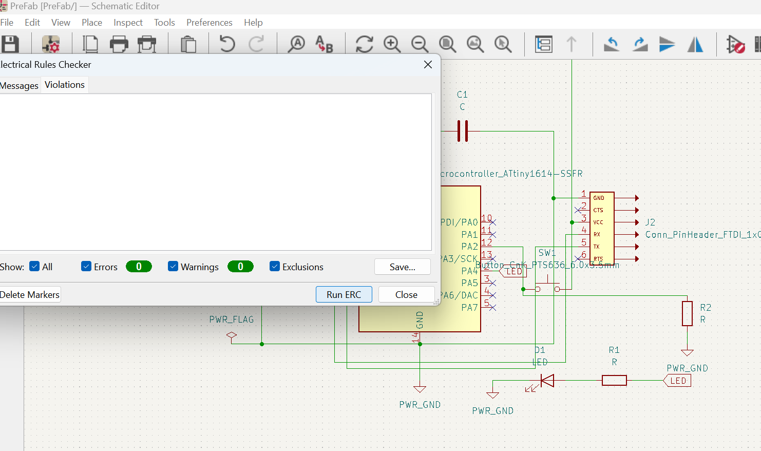
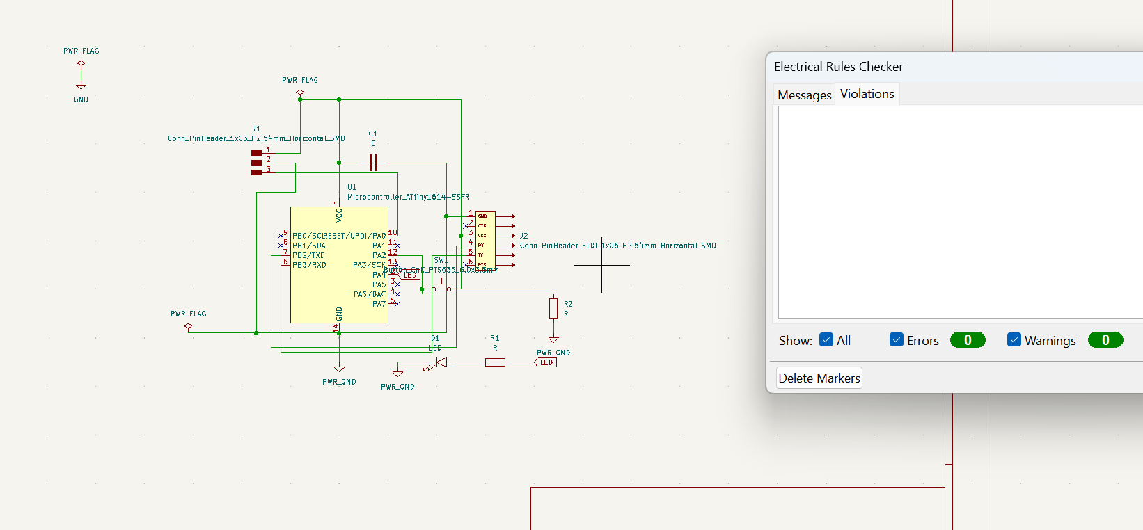
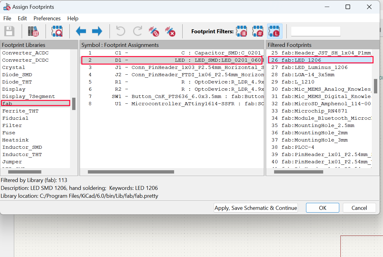
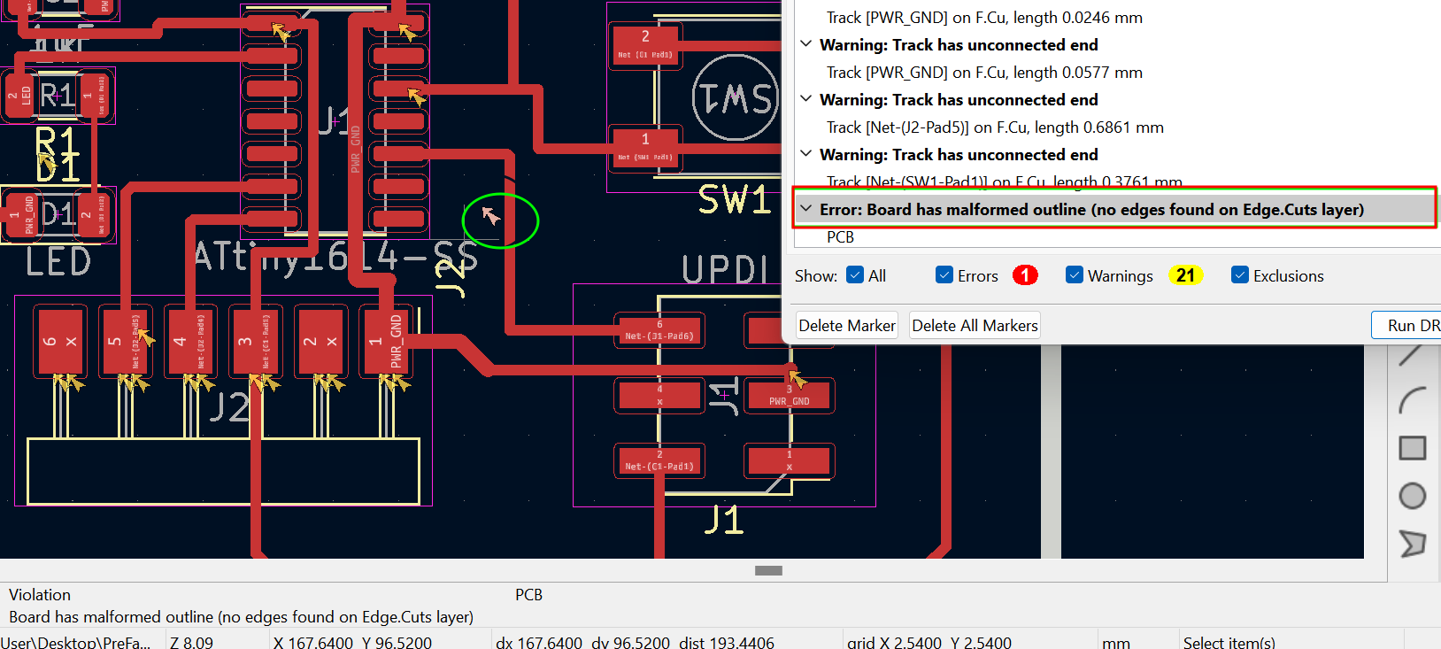
I had error is selection of components and had to redo the whole process from schematic to PCB editing. Therefore, added correct components from the fab library in schematic and then routed in PCB editor. Images of correct schematic diagram and PCB is shown below:Note:These are also available in Design Files.
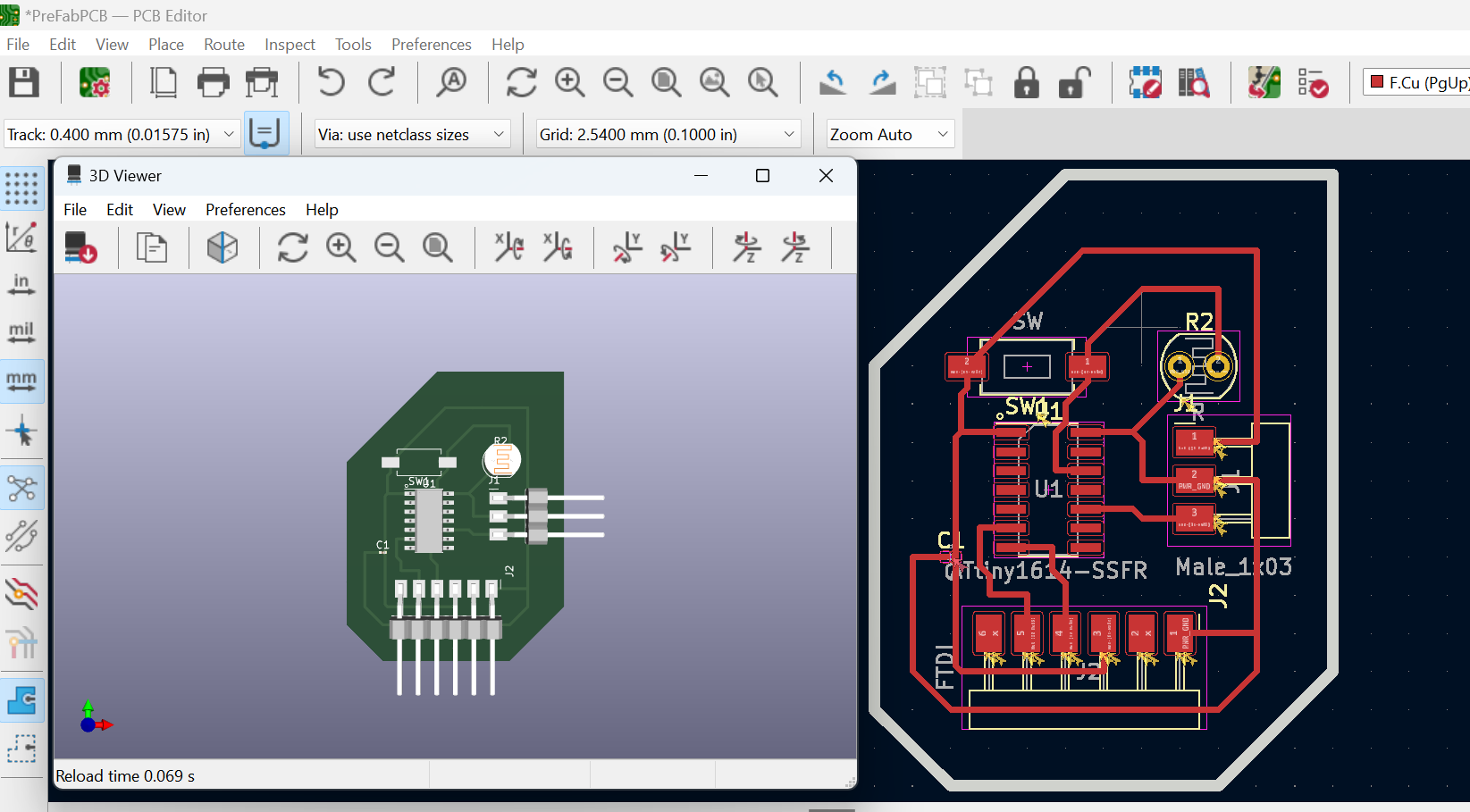
Saving and exporting your PCB board
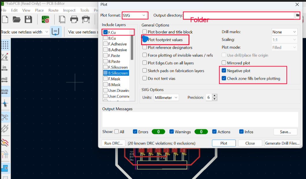
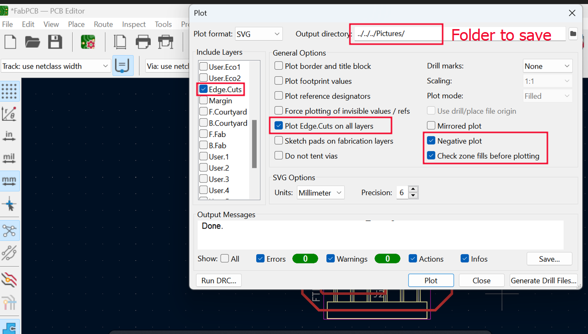
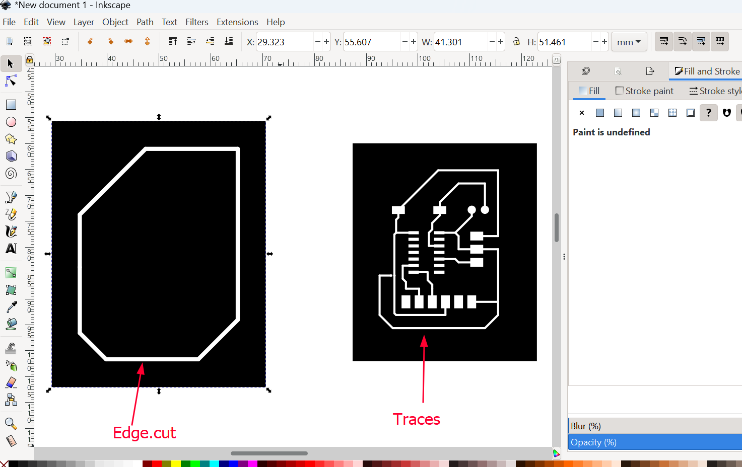
Editing SVG file in Inkscape after exporting SVG from KiCad
Open Inkscape and edit the SVG file you have created above and then Export in PNG format for which you can upload in the Mods to mill your PCB board. I have shown below the differences of Edge cut and Traces. Traces and edge cut uses different end mill therefore needs to be edited separately.