Electronics Design
According to Wikipedia, Electronic Design Automation also referred to as electronic computer-aided design (ECAD), is a category of software tools for designing electronic systems such as integrated circuits and printed circuit boards.
Task for Week 6
- Group Assignment
- - Using the test equipment in your lab to observe the operation of a microcontroller circuit board
- Individual Assignment
- - Designing a development board to interact and communicate with an embedded microcontroller.
- - Extra credit: Trying another design workflow, make a case for it and simulate its operation.
Group Assignment
Link to our group assignment is here
- This week, my job for the group assignment was to take photographs and videos of the work we were doing
- I helped in finding the right components to carry out our group assignment.
- I also used the multimeter to see the difference in voltage drop in different resistors.
Individual Assignment
- This week we are asked to design a development board to interact and communicate with an embedded microcontroller.
Eagle Software
- According to Autodesk, Eagle is a Electronic Design Automation(EDA) software that lets printed circuit board(PCB) designers seamlessly connect schematic diagrams, component placement, PCB routing and comprehensive library content.
- I used Eagle to draw my board.
- I had already installed the Eagle software in my PC. Here is the link if you want to download.
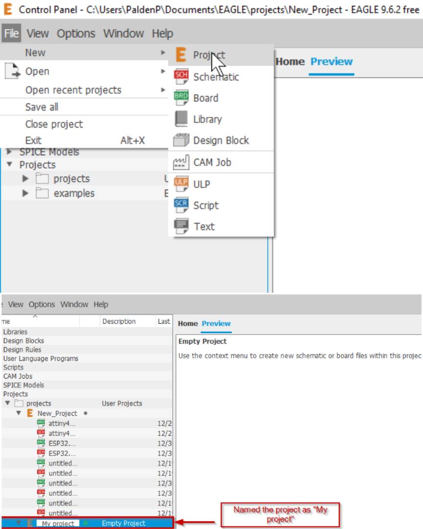
- After installing, I opened the eagle software and created a new file. To do that open eagle software → Click on files → new → Project and name your project.
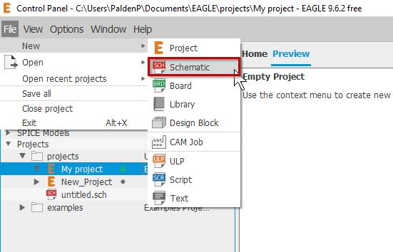
- Now once the project is created, go to files → new → schematics to create the schematic diagram of the circuit.
- You can get the Fab Library from here
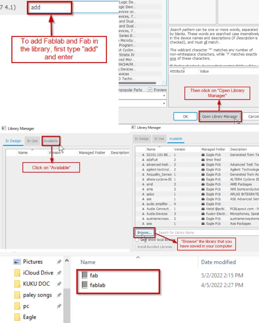
- Next, to add the fab library to the project, Go to Library → Open Library Manager → click on browse → select the fab library → click use.
- I did not find the ATTINY1614 in the Fab library. Had to search for it online. Finally came across a documentation of a previous student and the link for downloading the symbol and footprint is here
- Once I was done adding library, I then started to design my board. To add the components, type "add" on the text bar. Once we enter then a pop-up box displaying all the components shows up. Then search for Fablab and Fab, add the required components from there.
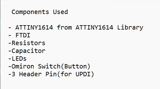
- For making my PCB board, I used the following components.
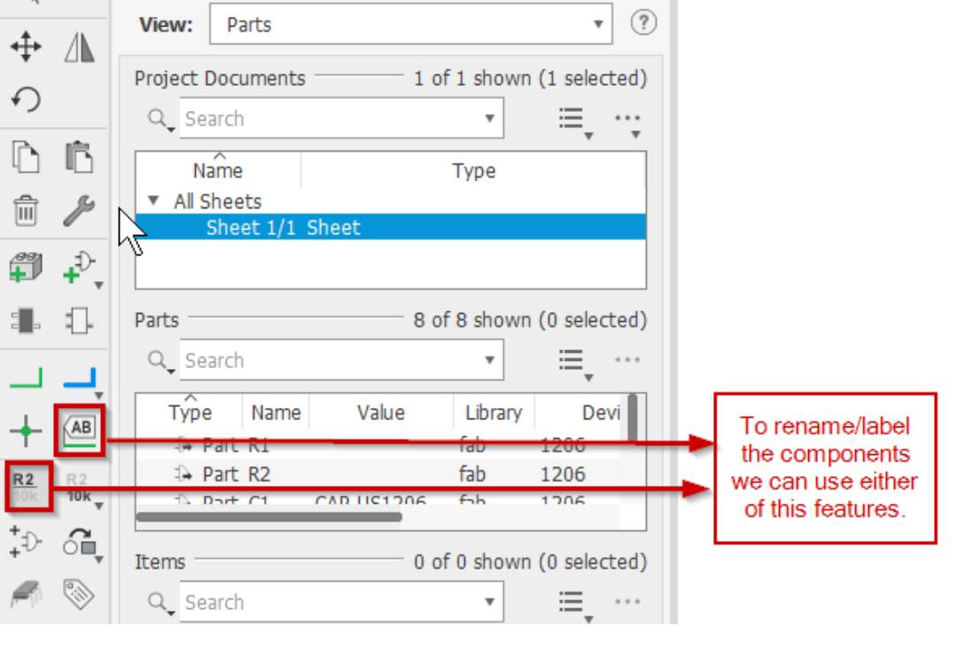
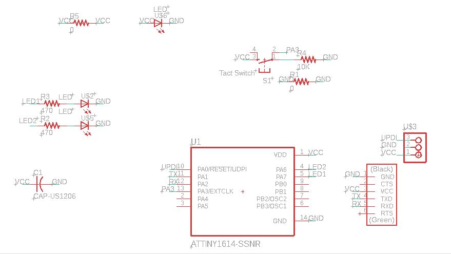
- Once I added all the components, I renamed each of the components and made the electrical connections.
- Referred ATTINY1614 pinout.
- Also Referred Attiny1614 board for electrical connections.
- Then was done with the schematic design.
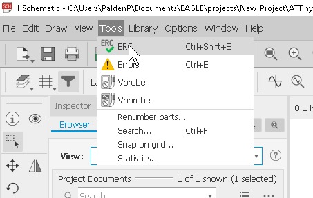
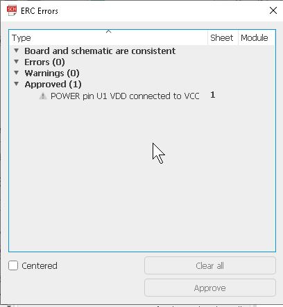
- After the schematic designing, run the ERC(electrical rule check).ERC warns us about any missing values of the components or any violations.
- To go to "ERC", go to "Tools" and then select "ERC" or short cut is "Ctrl+Shift+E"
- For components with no known value, we can approve it and go on.
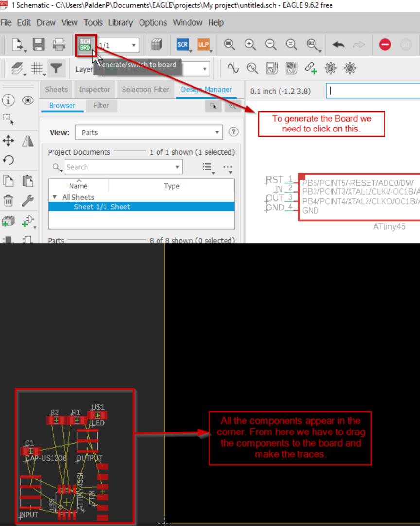
- Then generated the board design from the schematic design as shown below.
- Once I generated the board design, I moved all the components to the design window of the board design. I started arranging the components based on the best possible fit. Then I manually routed the connections.
- There were a couple of design rules I had to keep in mind when routing. First, I had to change the trace width to 10. I could do that by clicking the width option in the task bar above the design window.
- Our instructor informed us to ensure that no traces/routes run in between the controller pins and no more than 2 routes should run under any components.
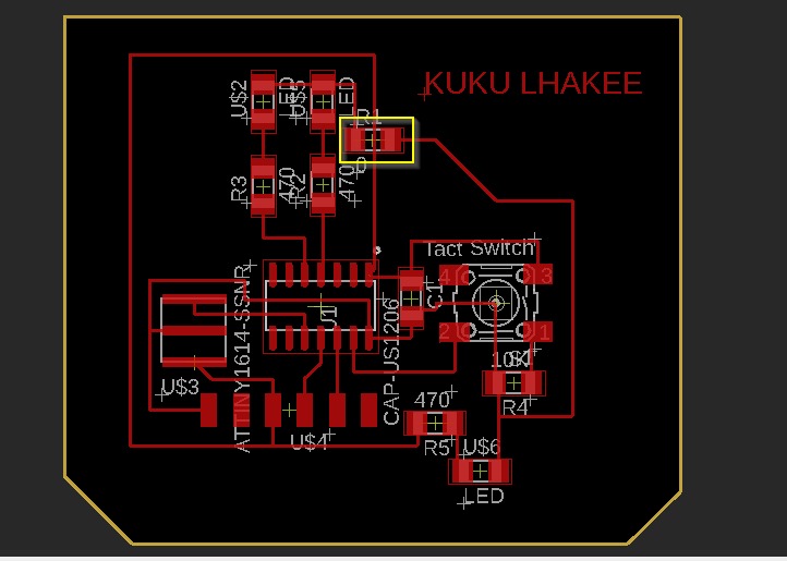
- I started routing and it took hours for me to optimize my board design to 100%. I added 0Ohms resistor to do a final routing between gnd since I couldnt find any other path way.
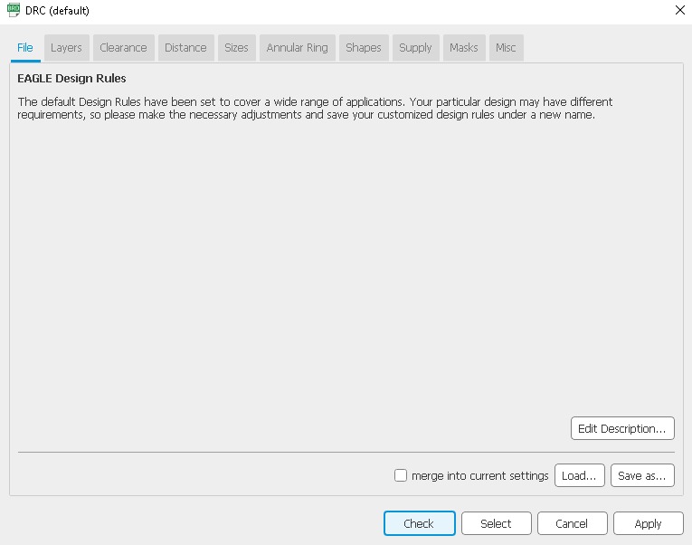
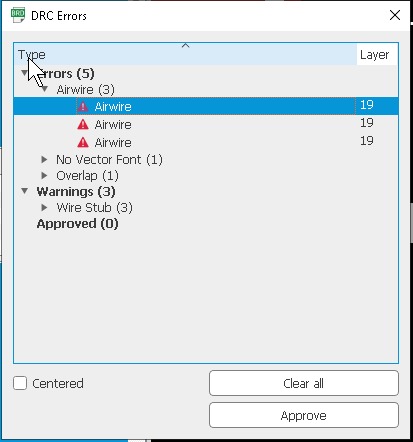
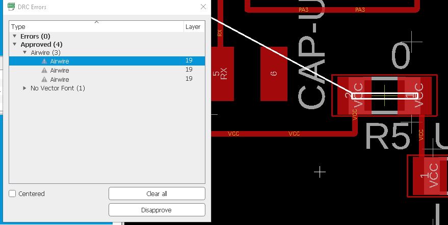
- After that, run the DRC(Design Rule Check) and I could see some errors.
- Corrected the errors and some airwires could be ignored hence approved them.
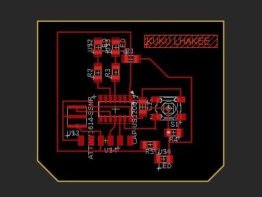
- Following is the final board design I made.
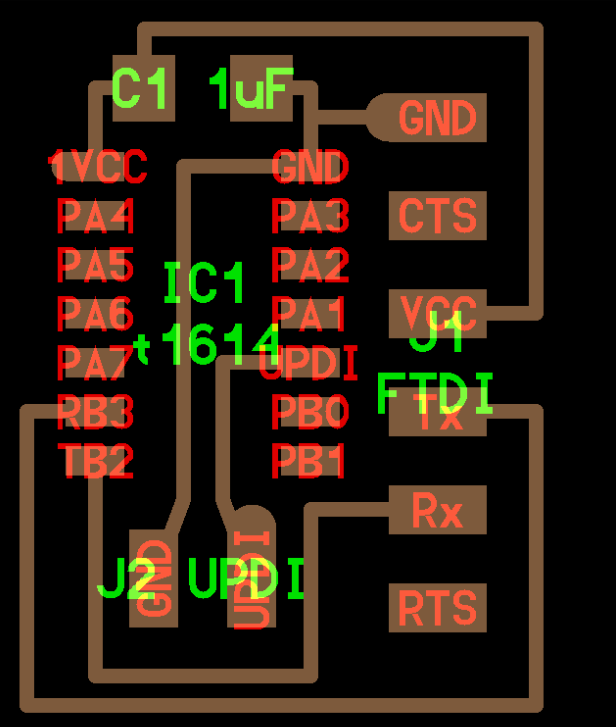
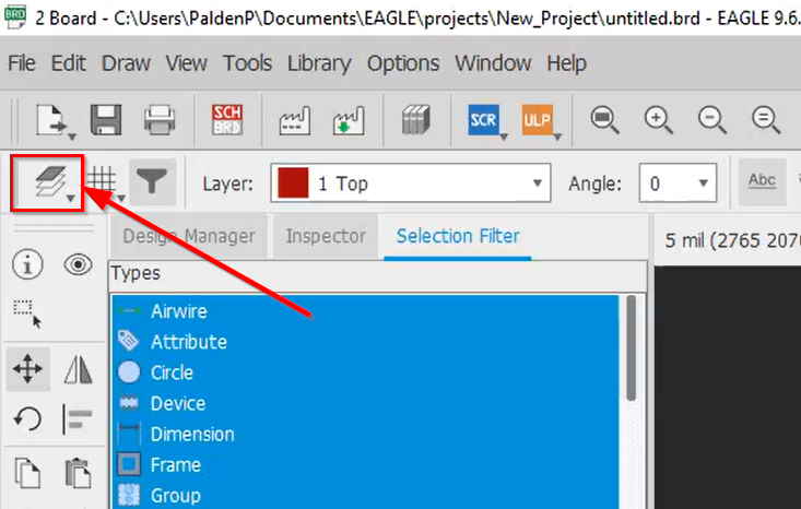
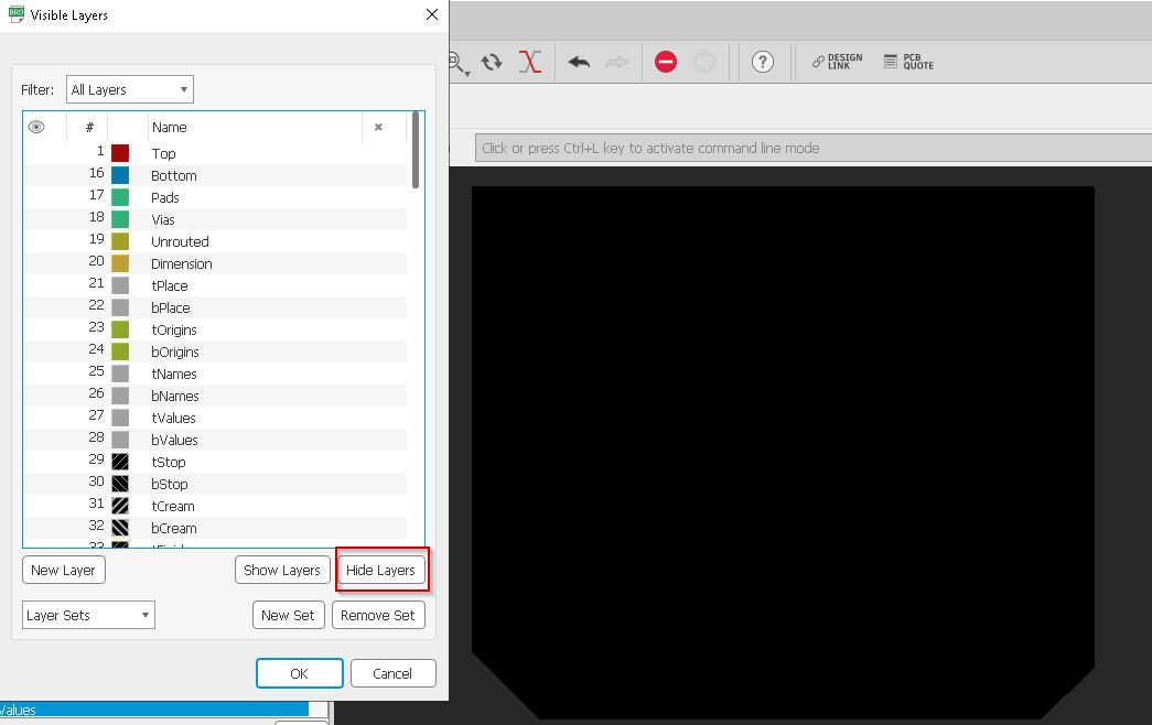
- Next I exported the board design as .png file. Before exporting, I removed the labelings on the components. This needs to be done to avoid issues when milling the pcb. To do that first Go to view option→ Select layer setting.
- Hide all layers.
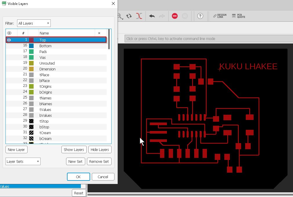
- To get the traces of the board, you can unhide "Top".
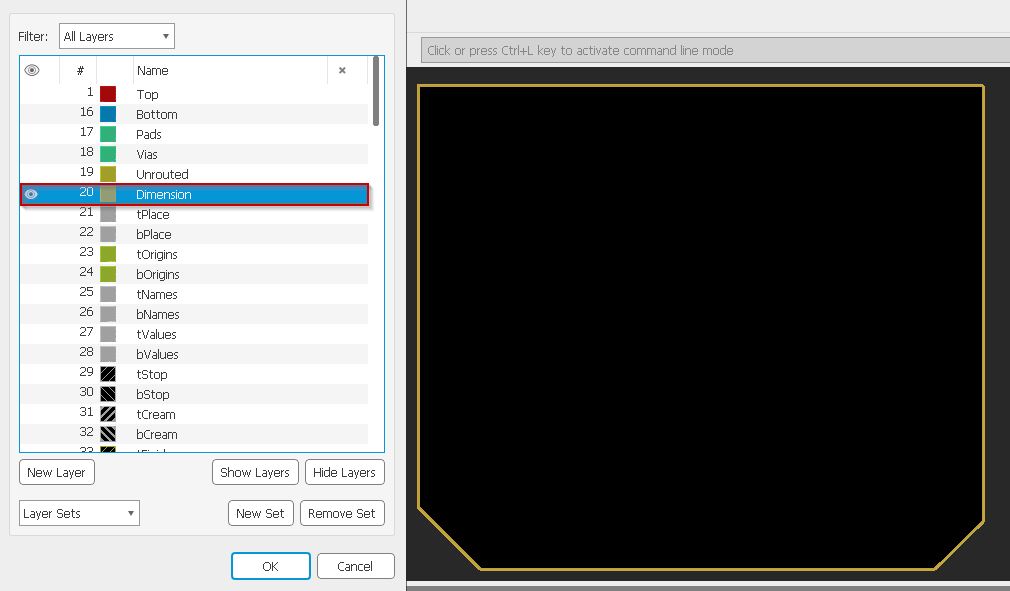
- Now to get the outline of the board, unhide "Dimension".
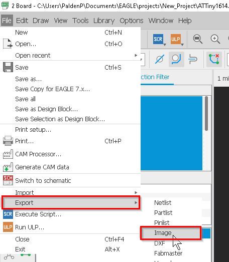
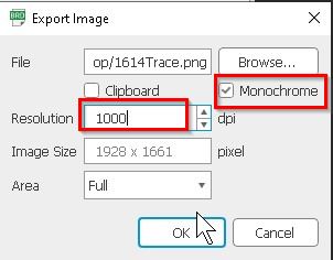
- To export the file in png format, first go to "File" -> "Export" -> "Images".
- Then a dialog box pops up, where you have to first choose the location where you want to save the file.
- Then Choose "Monochrome" and Change the resolution to "1000Dpi". Then click "Ok". The file will be saved in your PC in png format.
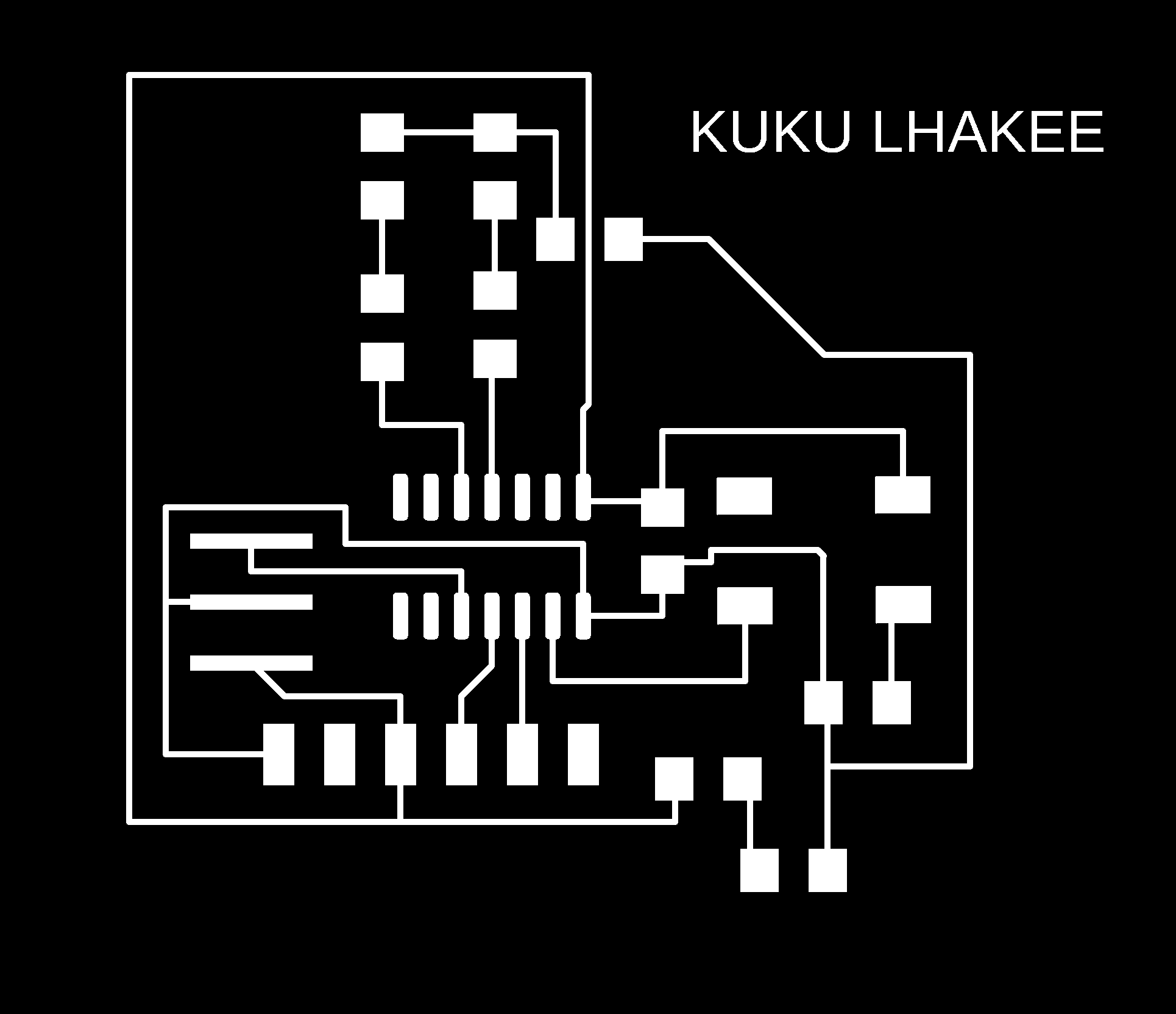
- My board traces and outline is shown below.
