Electronic production is the production (manufacturing) of electronics. This week, the electronics we are producing is our Printed Circuit Board. There are a few processes to build PCBs (Etching (acid), milling, copper cutting). There are also different types of PCBs, FR1 (the ones we have at Fab Lab Barcelona) and FR4.
Group assignment
At Fab Lab Barcelona we worked with the SRM 20 for cutting our PCB. In the group assignment, we understood that the machine doesn't operate so well when it comes to very small lines, so from .001mm to .010mm the copper not even stays on the board. Also, it seemed the endmill might be not very well attached when we did the test or maybe it was not so good the tip because the test board was full of "hair". Also, the outline didn't get cut completely, this might have been because we didn't do the Z-axis correctly.
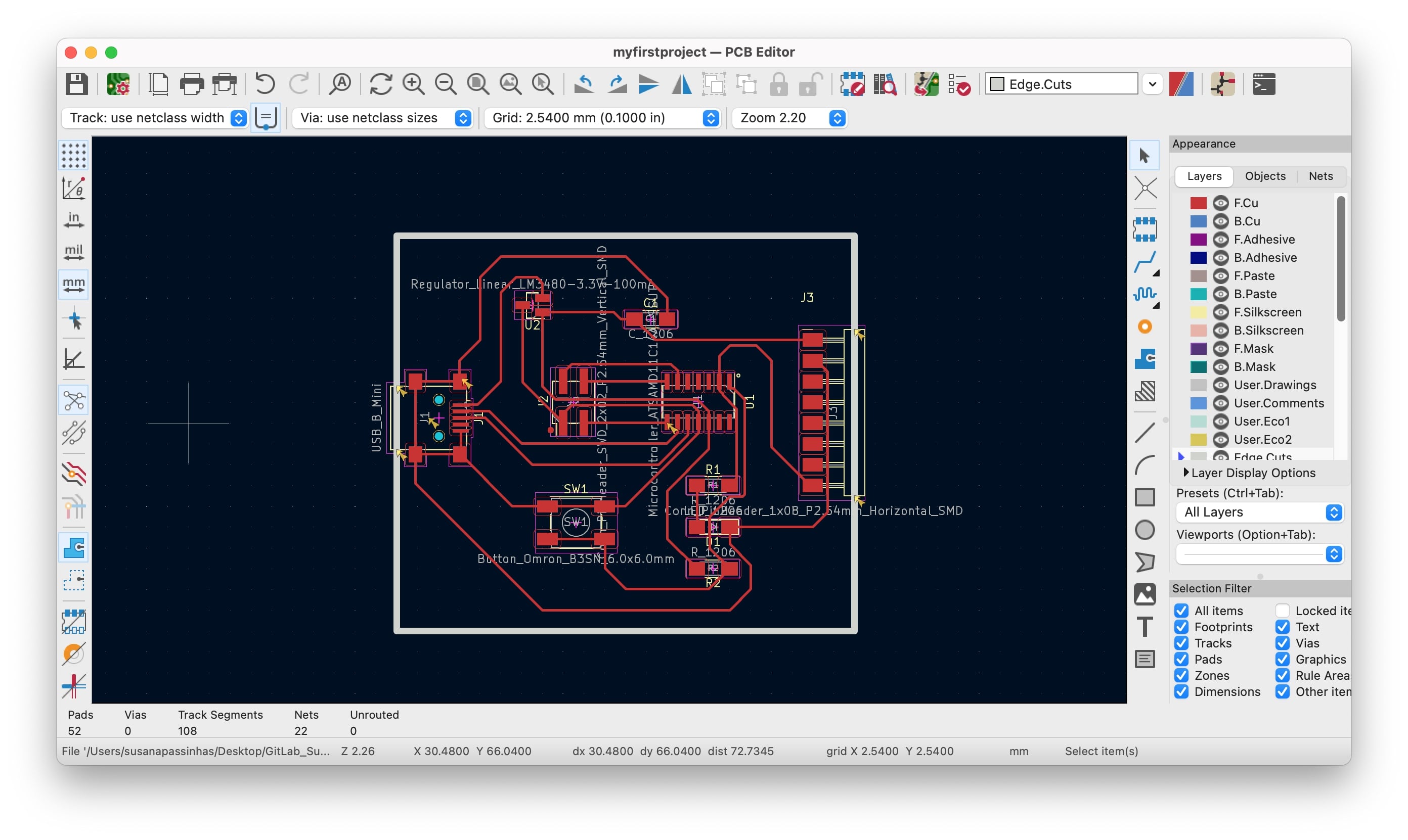
In this week's assignment, we needed to make and test the development board that we designed in week 6 to interact and communicate with an embedded microcontroller. So to start I needed to get my files ready for the SRM 20 machine.
Exporting the schematic SVG from KiCad
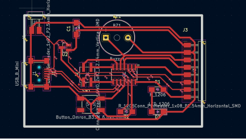
I started by going back to KiCad and double checked my schematic. I had previously made sure my clearance was 4mm (this is important to make sure the lines are not connecting and to have enough space to do the soldering).
I went ahead and added the outline cut. The outline cut will be the last thing to be cut by the machine (so it doesn't get loose while cutting the inside trace). The endmill to use for the outter cut is the 0,8mm endmill (1/32 inches) and it cuts through the board completely. So I added the outline square (white one here on the image) with a thickness of 0,8mm.
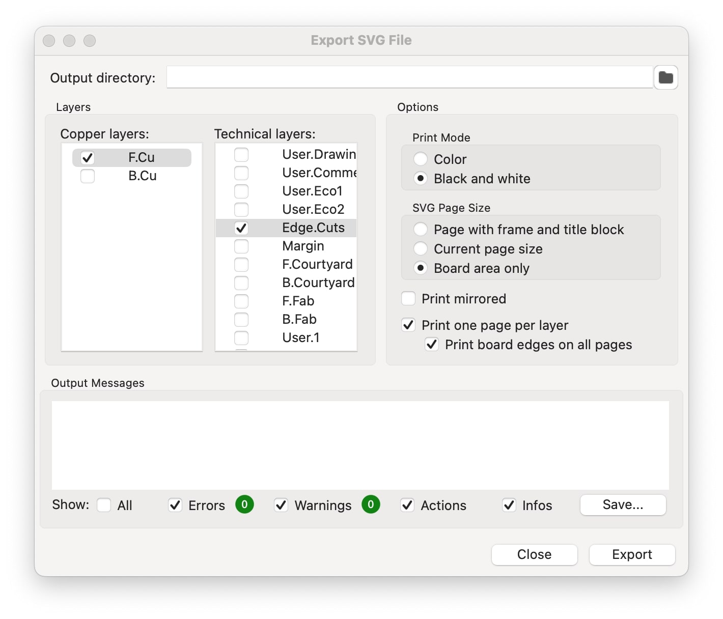
Then I just needed to export the file as an SVG so that I could edit it properly in one vector editor. To export it I selected the F.cu and Edge cuts (so I would get all the traces and outlines I needed).
Setting up the black and white per layers
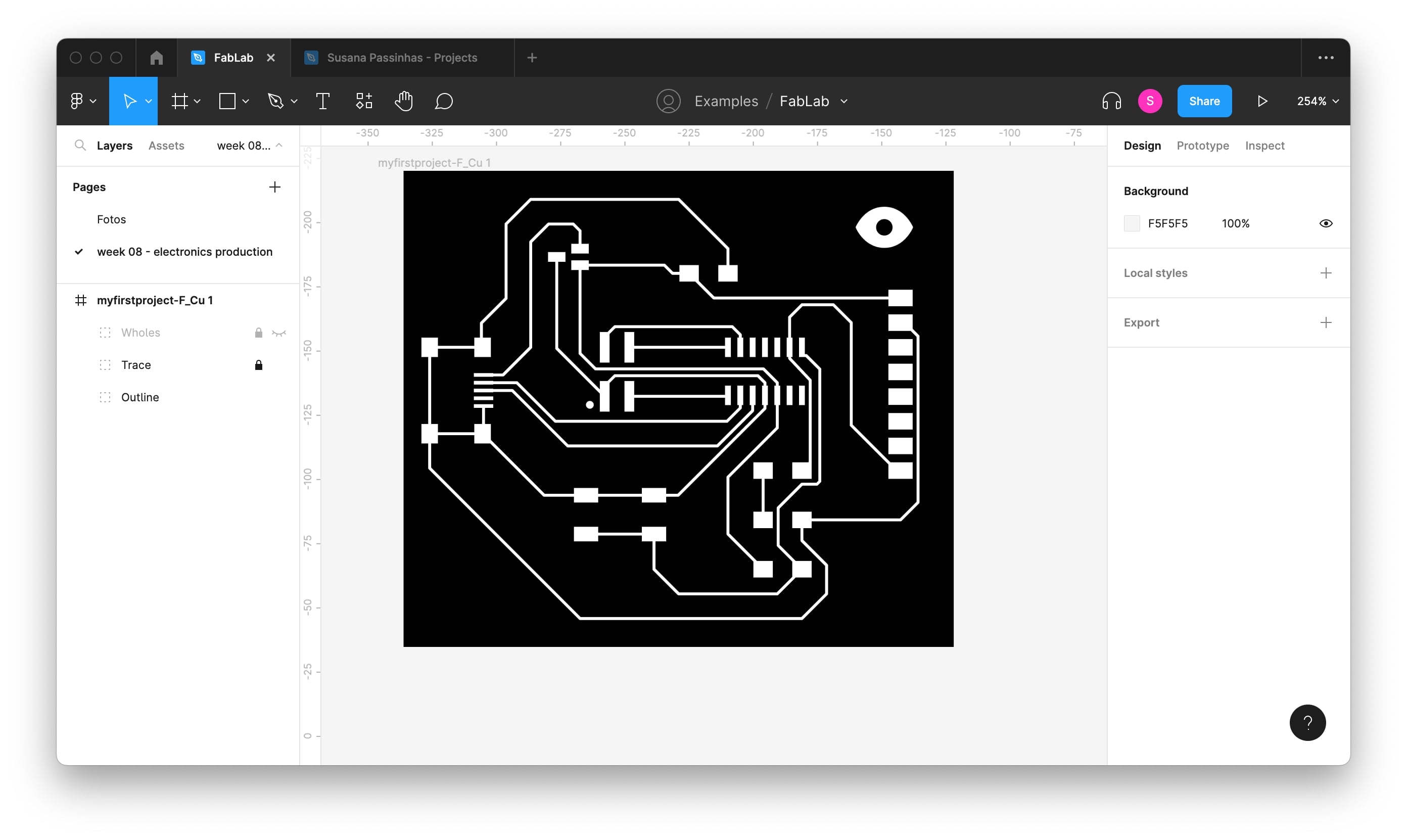
I opened my files in Figma and made sure to separate them by layers, one layer for the outline, another for the trace, and another for holes. In all of them, I made sure the black parts would be what is removed and the white parts will be what is not cut (the white it's the copper that stays and allows the circuit to be conductive).
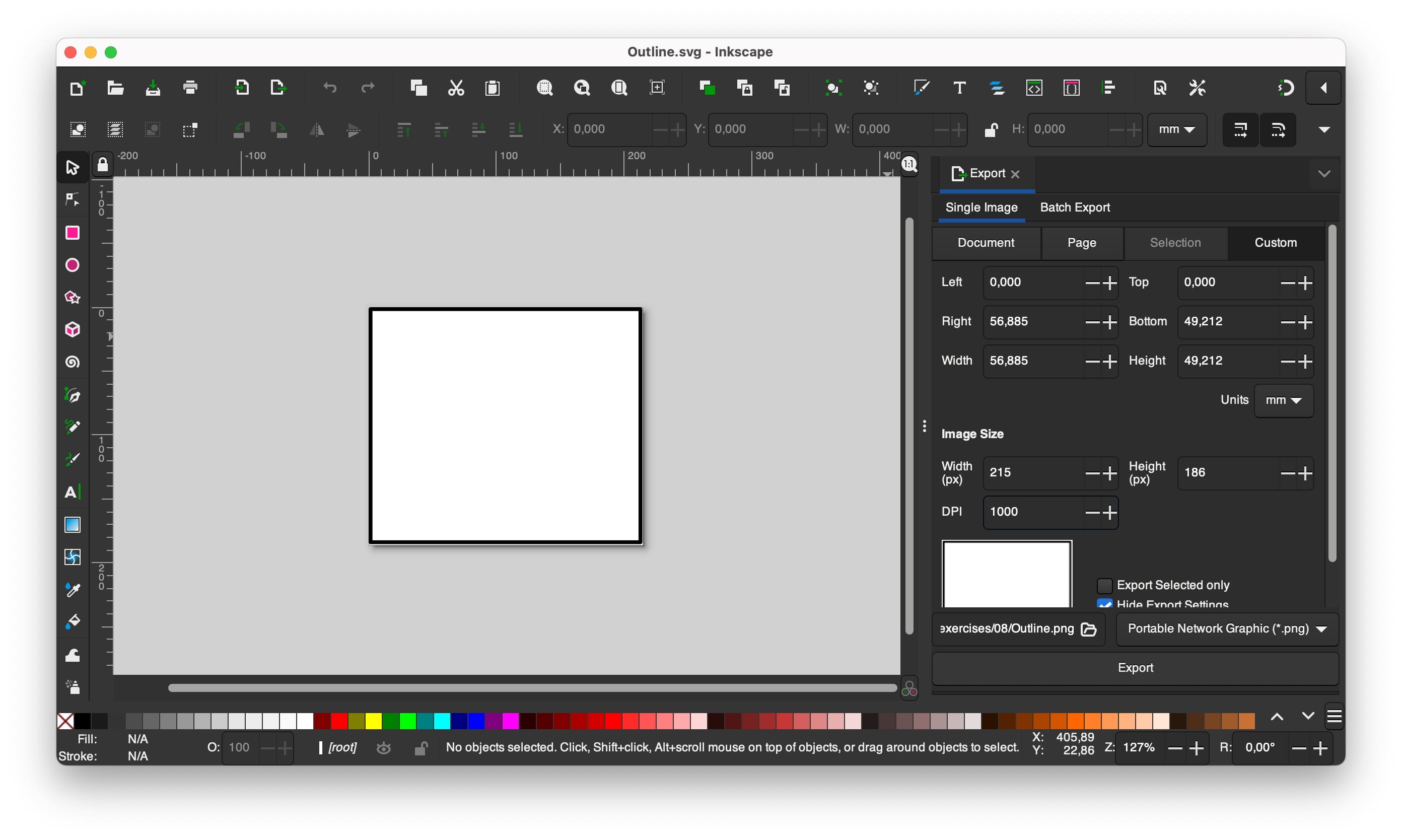
I also made sure my board design fitter the size of the board I was going to cut: 77mmx50mm. I then remembered about the resolution that I was not quite sure how to do it in Figma because a PNG is an uncompressed file, so I opened the SVG in Inkscape and checked the resolution, and set it up to 1000 so that in MODS it corresponds. The higher the resolution the better as the more detail the more precise the cut of the machine will be.
Preparing the file for the machine in MODS
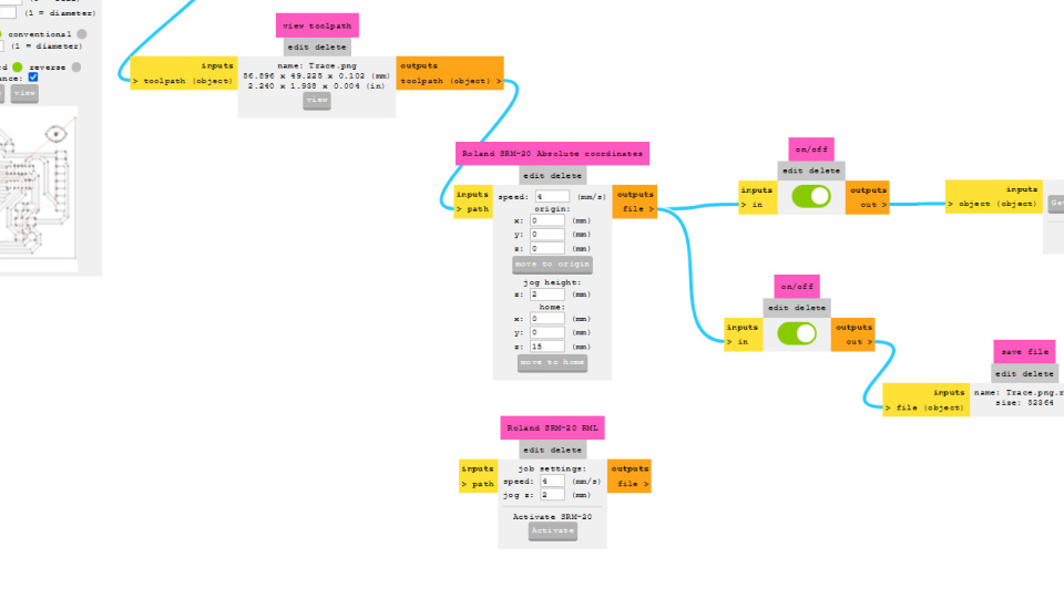
Once I had all my 3 images ready (trace, outline, and holes) I opened them one by one in MODS. In MODS I right-clicked and opened programs → open program → SRM 20-MILL → PCB.
Then I started the process of preparing the images: I selected the PNG file of trace first and made sure the dpi was 1000. Then in the "mill traces" I choose the 1/64 (0,4mm), the speed is set to 4 by default and that was the speed I used. In the job height I used also the default value of 2. The offset was 4 - the default value.
Then in the "absolute coordinates", I just wanted to make sure the "origin" x,y, and z were set to 0 and in the "move to origin" the x, and y were 0 but I set up the z to 15mm, to make sure that when the endmill is moving between points it doesn't scratch the PCB.
To end the process I just toggle on the "edit/delete" and click "Calculate". I also made sure I took a look into the trace to see if there weren't any weird lines overlapping.
For the holes and the outline I used the 1/32 (0,8mm) endmill instead. For the 1/32 endmill I used the default job height of 2 and the default speed of 4. The offset was 1 - the default value.
Once we click "Calculate" the software downloads the image in a format that the SRM 20 understands - the .rml format.
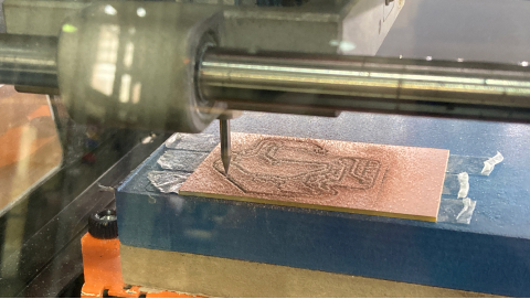
Cutting the PCB
Before cutting the PCB it's important to calibrate the machine correctly and clean the bed as well.
Calibrating the machine and setting up the correct endmill
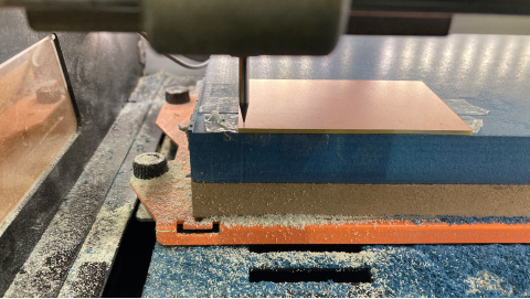
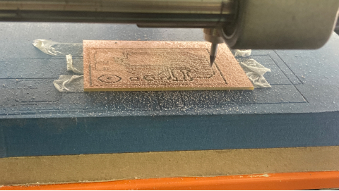
I started by passing a brush on the bed of the machine to clean all the dust and remove anything that might impact the cut. Then I choose the first endmill I was going to use. It was the 1/64 (0,4mm) to do the traces. I used the little key to help lock the endmill to the endmill holder.
I used a FR1 board (1 side copper) with a dimension of 77mmx50mm. I used double side tape glue to stick it to the bed of the machine.
I started by calibrating the x and y, so I moved the endmill to the 0 coordinates of x and y. Then I set up that position as the 0,0 (origin). After that I calibrated the z, this one is a little bit different since we don't want it to scratch the board while positioning it. So I drop the endmill close to the board and then used the key to loosen it a bit the endmill until it touches the board. I then set the z origin (0). Before doing anything else I moved the z position up to make sure it wouldn't scratch anything.
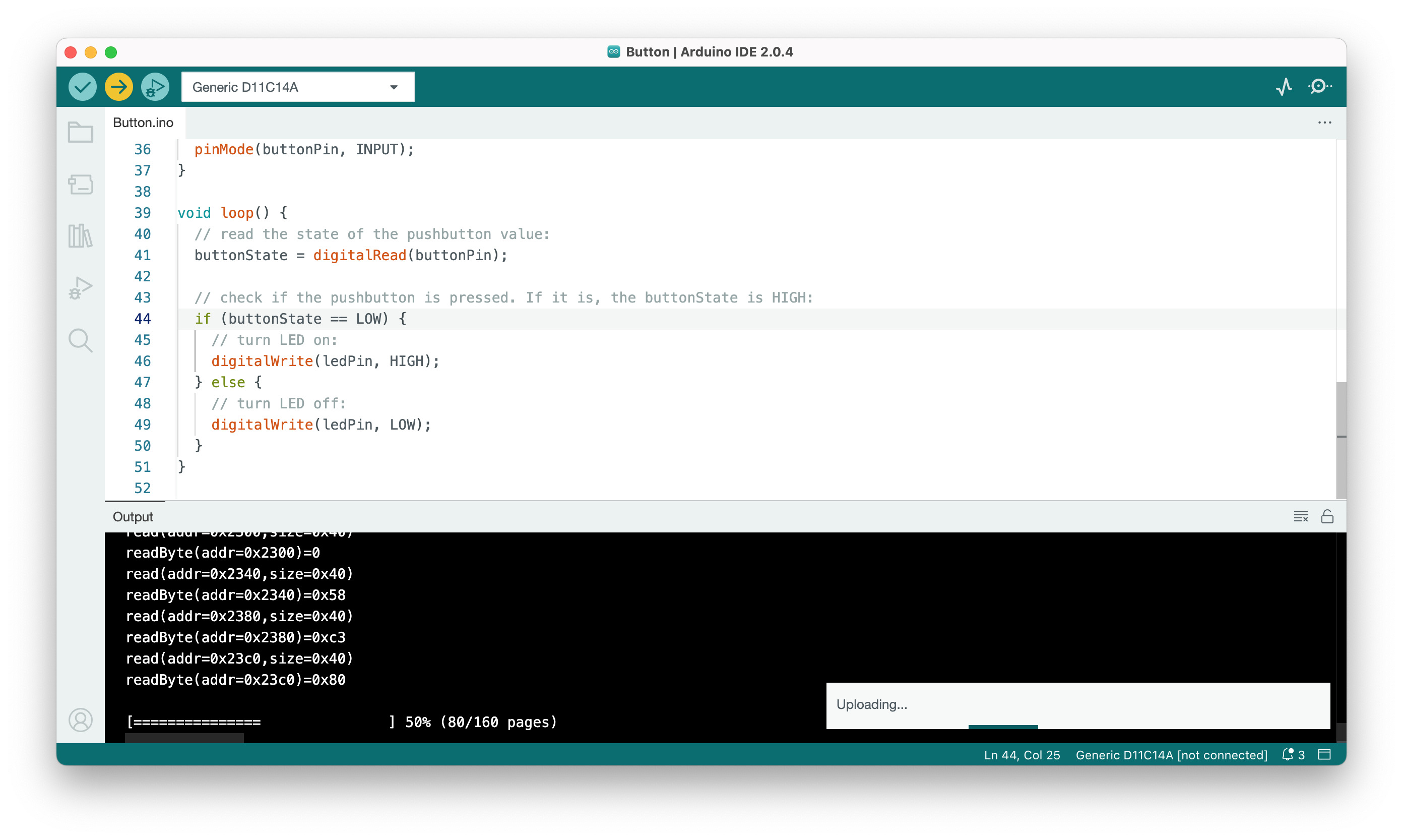
Then I had to add the file for the machine to cut (trace image first). I clicked "cut", then uploaded my image in the format the machine understands (rml), then I just pressed "output" and the machine started to cut.
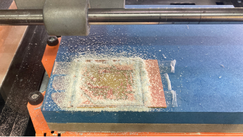
Milling
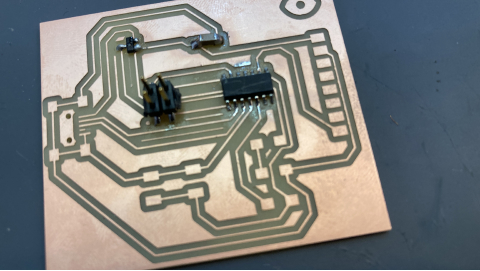
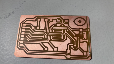
I first cut the trace, using a 1/64 endmill. When it was finished I replaced the endmill to a 1/32 and added the holes file. I did the same process as before to calibrate the machine again but this time only for the Z position. Then I did the same but this time for the outline. With this sequence, we make sure there aren't any loose pieces on the machine.
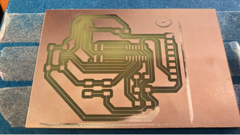
The result...
After the first cut was finished I cleaned and dusted and realized there was something strange, it seemed that in some places the machine didn't cut so well because I still could see the copper (it might be some dust for example). So I repeated the entire process again and this time it came out well!
Soldering the components to the PCB (WIP)
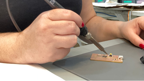
To do the soldering we need a wet sponge or the wire scouring pad to make sure we clear the tip of the soldering iron at all times (this cleans the tip very well). The temperature to use is between 350-400 degrees (I used 350 degrees). I also turned the smoke extraction on (a little machine that we have at the table).
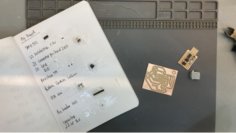
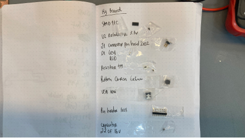
The components
Before starting the soldering I grabbed all the components I needed for my board. I double-checked Kicad to make sure of the components I needed.
List of components
About the capacitors and voltage regulators:
A capacitor is an electrical component that draws energy from a battery and stores the energy. So it stores energy until is needed to be released. Using a 2.2 uF means it is safe to use this capacitor upto 400v. We are using 5v in our DC board.
A voltage regulator is a system designed to automatically maintain a constant voltage. This is used so that the LED and the Button don't burn (shortage) the board.
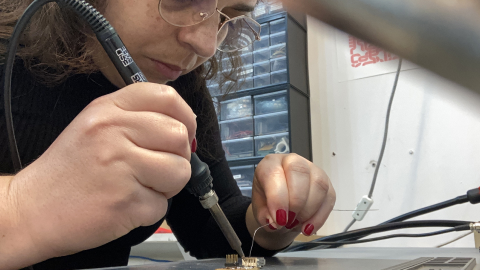
Soldering
Before I start to solder in my board I decided to practice on an old board. I worked with a temperature of 350 degrees and make sure to clean the tip of the soldering iron frequently.
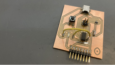
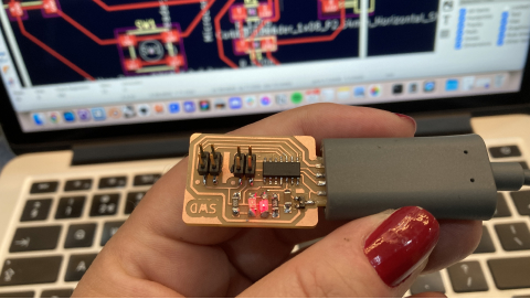
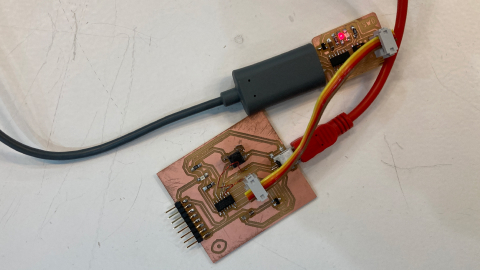
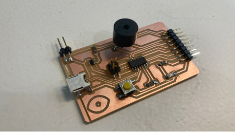
Then I was ready to solder my board. So I started with the SAMD 11 first because it was in the center and it was more complex due to the tiny legs. I continued and then realized I had soldered the SAMD 11 reversed...So I needed to un-solder it. I used the removal wire we have to remove the biggest part of it, but still was not coming out completely, so with some help, I used the heat gun to heat up the SAMD 11 and pulled the component out with the claws. Because of this, some wires got erased, so I re-soldered again the SAMD 11 and had to connect jumpers.
Checking if the circuits were working
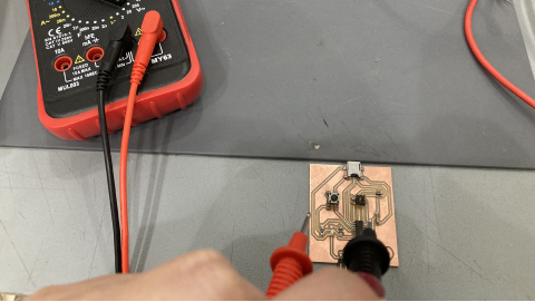
I used the multimeter to make sure all the connections were working. To do this I simply used the bip function and then connected the wires to my circuit making sure the current was passing on the places it was supposed to pass.
Coding
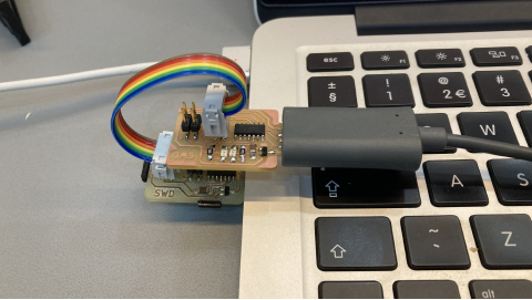
So now it was time to code my board. But before I could code my board I need to tell my board that she is programmable. To do that I needed to use a bootloader. At the Lab this week, not only I manufactured my own board but also a SWD board to be the programmer of my own board. So I add to bootload the SWD so that I could use it as a programmer for my new board - meaning I can bootload my new board with this board (the new board though only receives the bootload so she knows she can be programmed but she does not intend to program any board).
Bootloading the SWD board first
At the Fab Lab we have already a SWD D11C that can act as a bootloader (a programmer). So I used it for the new one I just had soldered.
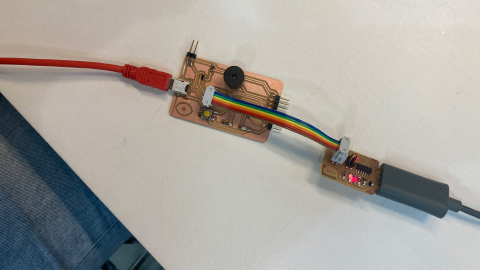
So, to start I needed a wire to connect both SWDs, the connector at the lab has 6 wires but we only need to use 4, so we need to make sure to use the same 4 ones. Also the PCB board is a little thin for the USB so I added a piece of paper to make it fit properly.
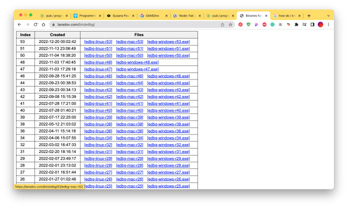
Then, for the code I went to the page with all the information we need to follow. Then I downloaded the binary file that will make the board a programmer - free dap.
To flash the board we also need the edbg (edbg is a software that allows us to program the board). I choose the latest version of the edbg for my mac and downloaded it.
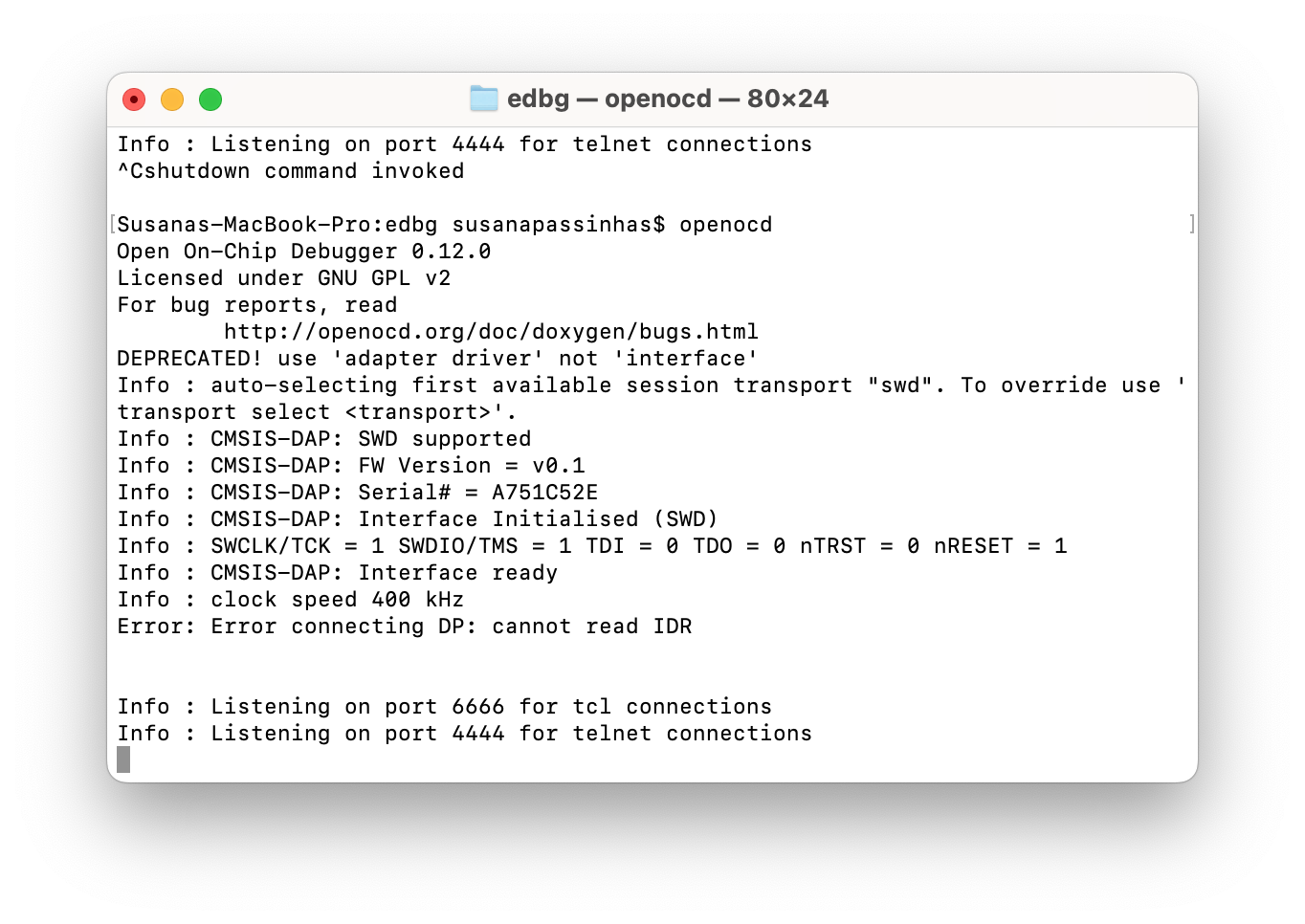
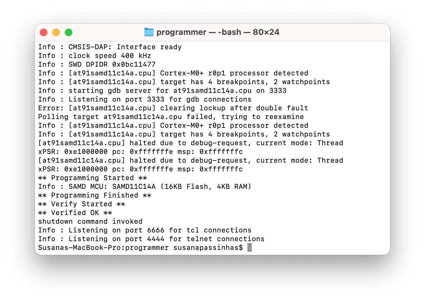
Then I opened the terminal and used the command "./edbg --help" to see what options I have with this file, but the terminal replied with "permission denied". So I went ahead with the option to flashing on MacOS...
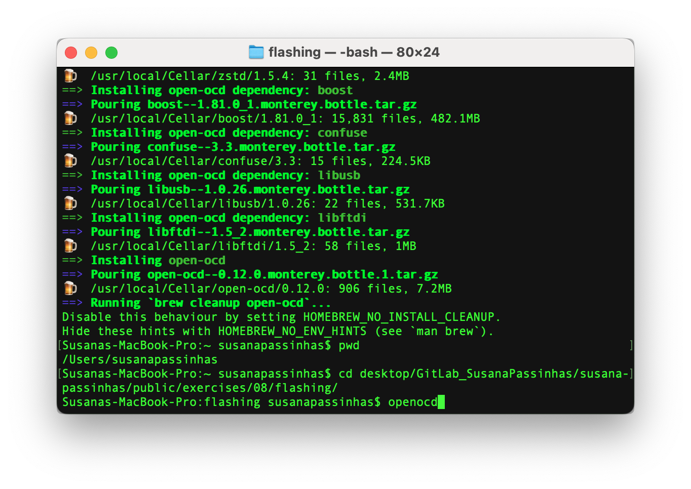
Using openocd (MacOS) instead of edbg
When the edgb firmware doesn't work on MacOS we can use OpenOCD. I used Homebrew to install OpenOCD using the command "brew install openocd". Then I created a new directory with the downloaded configuration files for the Open OCD and also added the free dap (previously downloaded) file there.
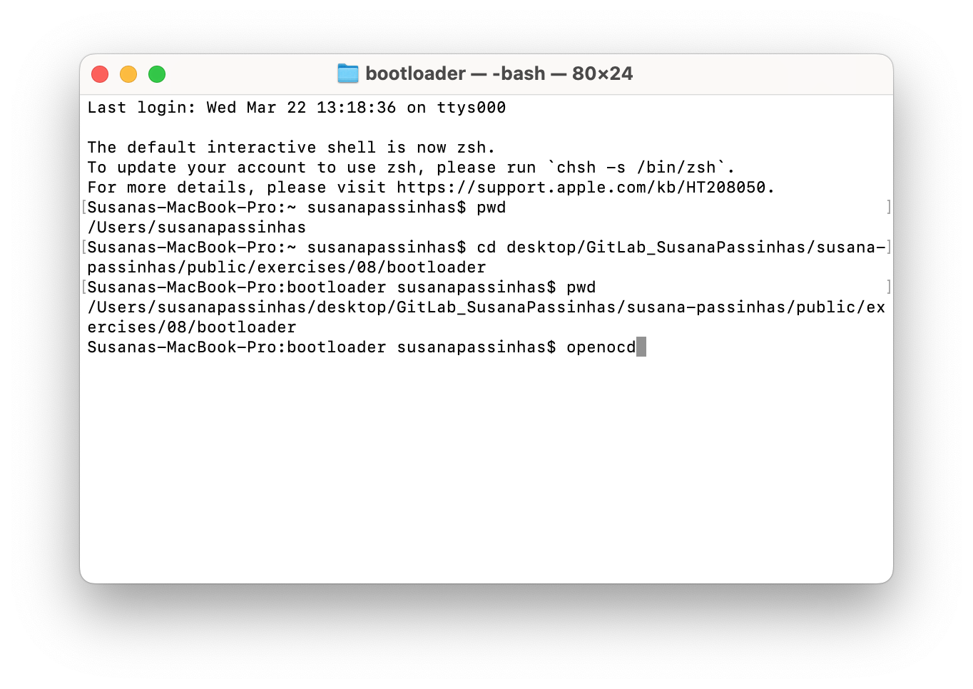
Then I used the terminal to navigate to the directory and run the command "openocd".
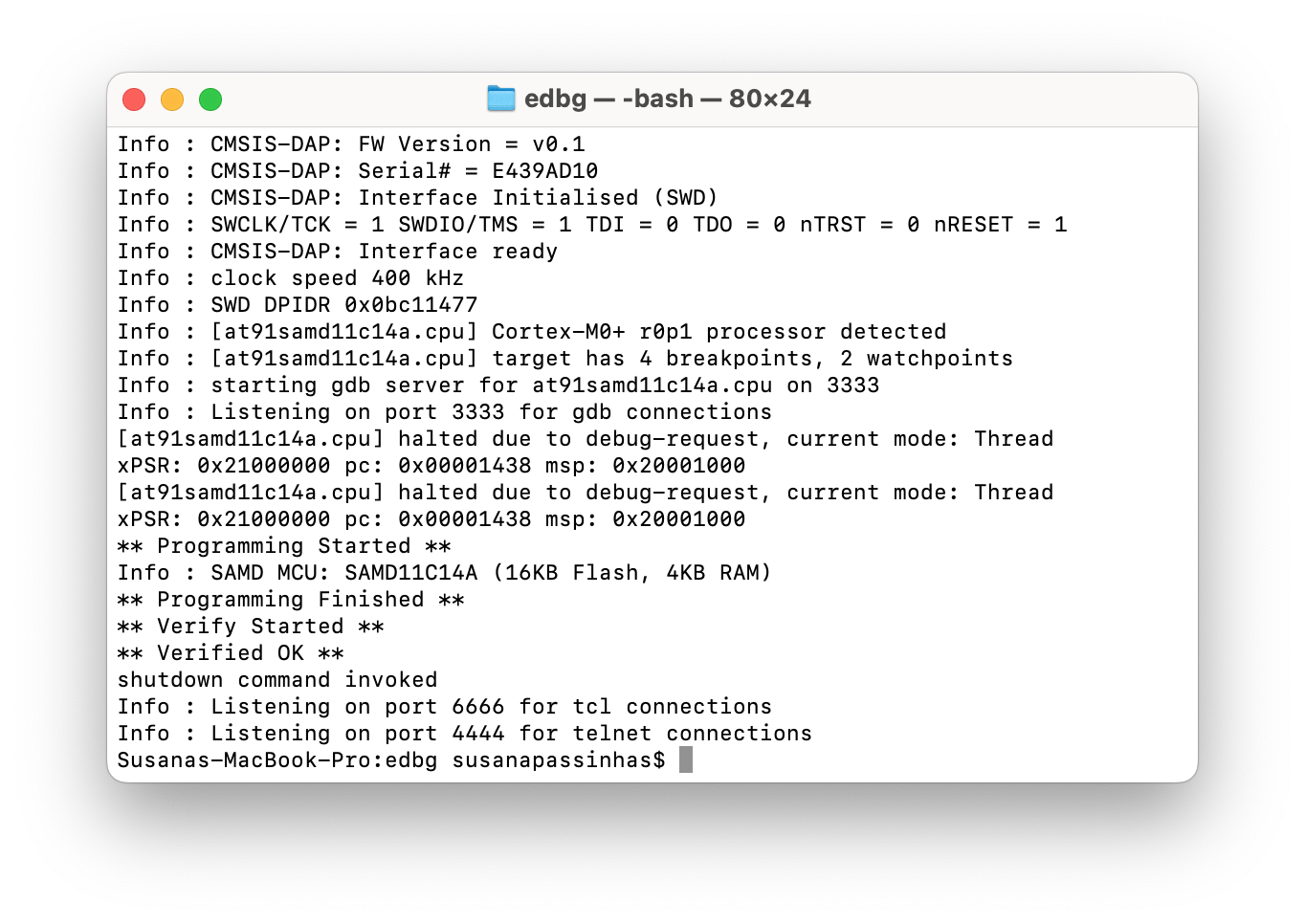
Getting the SWD bootloaded
I tried a couple of times doing the bootloader and it was not working at first because the computer didn't recognize the new board (had no problems with the board I was using to bootload it). Then after improving the soldering and trying again, it was possible to burn the bootloader into the SWD board I manufactured and now I could use it as a programmer for my own board. At this moment I also realized I had a LED reversed (was not connecting the GND to the GND), so also update that.
Making my own board programmable
So now that I had my own bootloader I could flash my own board. So I used the same 2x2 IDC connector, keeping the orientation consistent (so that the ground marks are on the same wire). This time I needed to change the pinheads from the SWD, so instead of being the bootloader pins I used the programmer pins (the ones close to the edge of the board) and connected them to my own board.
To program the board we now needed to use a different file, so I went ahead and downloaded it into a new directory. Then I needed to open the terminal and after navigating to the correct directory using the command "openocd".
It seemed like the board was programmed but I couldn't recognize it in the Arduino IDE...so I went ahead with the help of the instructors to try to debug it by double-checking the connections with the multimeter, re-soldering components, making sure they were well soldered and nothing... I spend quite some time on this. Then I decided to go back to kicad and double-check everything.
Re-designing and manufacturing my board (again)
When I open Kicad I realized I actually had a few pins without a connection... when I double-checked SAMD11 I also realized I had 1 pin wrongly labeled! So I updated my schematics, but because this week extend to week 09 I actually re-designed it to accommodate a piezo sensor (buzzer). So I just added the symbol for piezzo (12m), connected + to a PIN, and the - to GND. Then I went ahead and cut and soldered the board again.
Trying to program it!
So the good news was that now the board seemed to be recognized by the computer! So I went ahead and sent the code (SAM BA file) to make the board programmable using the SWD board I have done before.
The bad news was that in my MAC I still couldn't see the board in the Arduino IDE...So I tried in a colleague's Windows and it was recognizable (on and off) so it seemed maybe the soldering was not working so well or maybe there was a shortage... Which actually ended up being the case!
With the help of FabLab instructor, we soldered a new SAMD 11 and removed the piezo sensor as it might be doing some shortage (and it was! since without it the MAC recognized the board and with it it didn't). Without the piezo sensor on the board finally, after a few boards, a lot of debugging, and soldering the board was working! Arduino IDE recognized it and I could send the code when pressing the button to light up the led! What a moment of joy!!!!
This week(s) were really tuff... It was a lot of debugging, soldering, re-soldering, a lot of mistakes, a lot of cutting and a lot of trying! I really learned how sensitive the components are and how important is to solder things properly...
On a positive note I thought that the CNC we used is much easier to handle than the big CNC, so that went really smoothly. I did though cut my finger on the edge of the board, but that was silly of me (I went with my finder to clean a bit of dust right on the edge of the board) and also ended up burning my finger. I also understood how sensitive the machine can be since we are cutting 0,1mm measurements...because the first board didn't come out right and I assume it was just because there was something on the bed... probably because I did exactly the same thing for the second board and that one came out right!
When it comes to the soldering I found it actually quite peaceful, it's really challenging to handle such small components but somehow it gives peace trying to hold them and put them in place. I also realized I need to practice this much more, since I had quite a lot of trouble with things not being well soldered (still didn't quite understand what I was doing wrong).
I did found it a bit overwhelming looking for the specific components in the immensity of drawers we have with them, but I think this is just because it is new and I am not used to their names. Definitely need to feel more comfortable with this.
I went through a lot of os mistakes that I could have prevented if I simply had spent much more time checking and double-checking everything. Nevertheless, at least I got experience in everything! Re-soldering, debugging, re-cutting, double-checking schematics and datasheets, and so on.