Susana Passinhas @Fab Academy 2023
06. Electronics Design
To understand what electronics design is we first need to understand how electricity works. Electricity is a movement of charge. Objects can hold an electric charge. We keep listening that everything is energy, well we can say that because atoms have electrons (negative charge) and protons (positive charge). Protons attract electrons and when we put them together they will always try to equilibrate.
We can produce electricity by pushing electrons in the same chain direction (going through conductive material), once you push the first electron we push them all. This is called an electrical current. We have 2 types of current, AC (Alternate current), which is always changing between positive and negative, going back and forward (the frequency alternates), usually 220V, and then we have DC (direct current), which is either negative or positive and goes in one direction, 5V onto ground (0V). This is the current we use for our electronics design project.
Electronics design is the design of a circuit, and how it works so that after we can produce it into PCBs (printed board circuit).
Group assignment
A multimeter is used to debug electronics, it can read a lot of things: olms, hertz, volts, and volts of alternate current. We can use it for example to check continuity if points are connected together. To use it we can set up the scale, for example, if we set up the scale to 200volts it will read everything below it. Also, we have 2 cables, 1 black, and the other red, usually, the black is negative, but not always, depending on the manufacturer, so we can know this by simply checking if the value shown on the screen has a "-" in front means we are using the negative for positive and positive for negative so we just need to swap the cables connection.
An oscilloscope is an instrument that graphically displays electrical signals and shows how those signals change over time. Engineers use oscilloscopes to measure electrical phenomena and quickly test, verify, and debug their circuit designs. The primary function of an oscilloscope is to measure voltage waves.¹
We learned how important it is to use the multimeter when it comes to debugging. With the multimeter we can check if the current is actually passing, therefore we know if the circuit is working or not. Also, we can measure how much current is passing so we can make sure we are using the correct components for example (for example to check if the voltage regulator is correct as it is supposed to change the voltage feed into the PBC).
→ Group Page here
Design a development board to interact and communicate with an embedded microcontroller
For this assignment, I worked with the SAMD 11 microcontroller. This is one of the microcontrollers we use here at Fab Lab Barcelona in our Barduino board. This microcontroller allows communication through USB, very useful to connect with a computer to upload code into the board.
There are quite a few programs in the market that allows us to design circuits so that we can produce PCBs (printed board circuit): EAGLE, Flux, and KiCad, among others.
KiCad
For this project, I have worked with KiCad, an open-source and free-to-use software that is nicely maintained and easy to use. KiCad has a Schematic Editor where we basically add all the components we will need to create the circuit. It also has a PCB Editor, where we connect the components to each other - we create the electric circuit here.
Adding extra libraries to KiCad
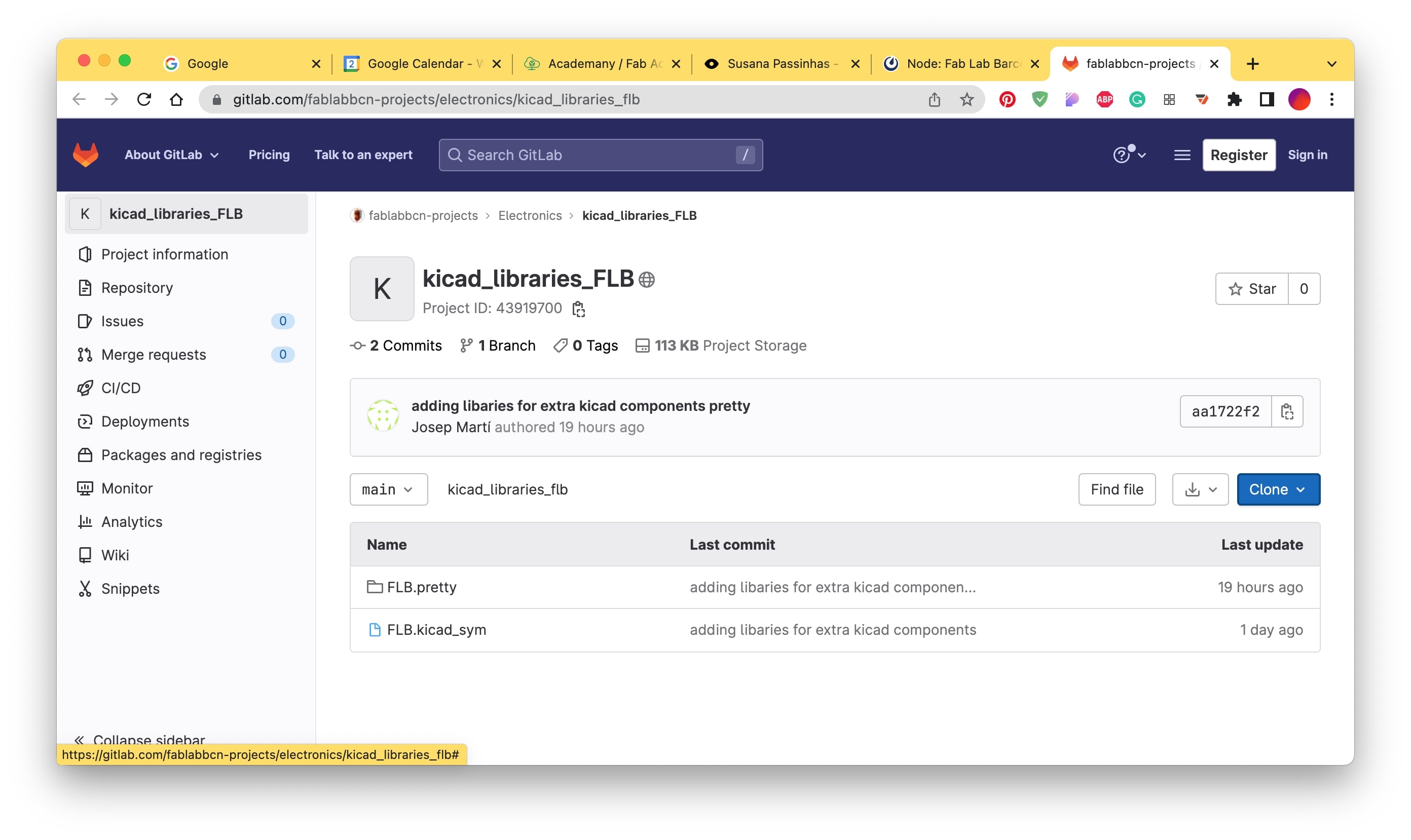
KiCad works with libraries, meaning it has the details of quite a lot of components that might be used in a PCB. Though we needed to install extra libraries for the microcontrollers we have in Fab Lab Barcelona. To do that I just went to GitLab and cloned the repository of the Fab Lab Barcelona components library on my computer so that I can add it to KiCad. We can add new libraries in KiCad by going to preferences > Manage symbol libraries / Manage footprint libraries and adding them by simply connecting the cloned repository. The symbol library refers to the components themselves and their details, the footprint refers to the visualization of the areas we will need to consider when it comes to soldering it later in the PCB.
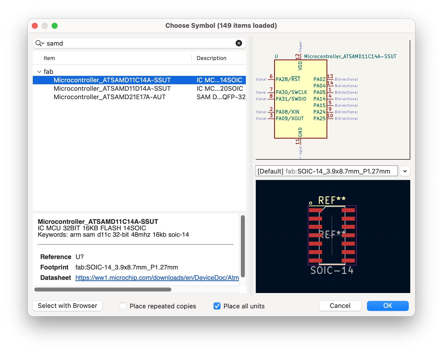
Adding components - SAMD 11
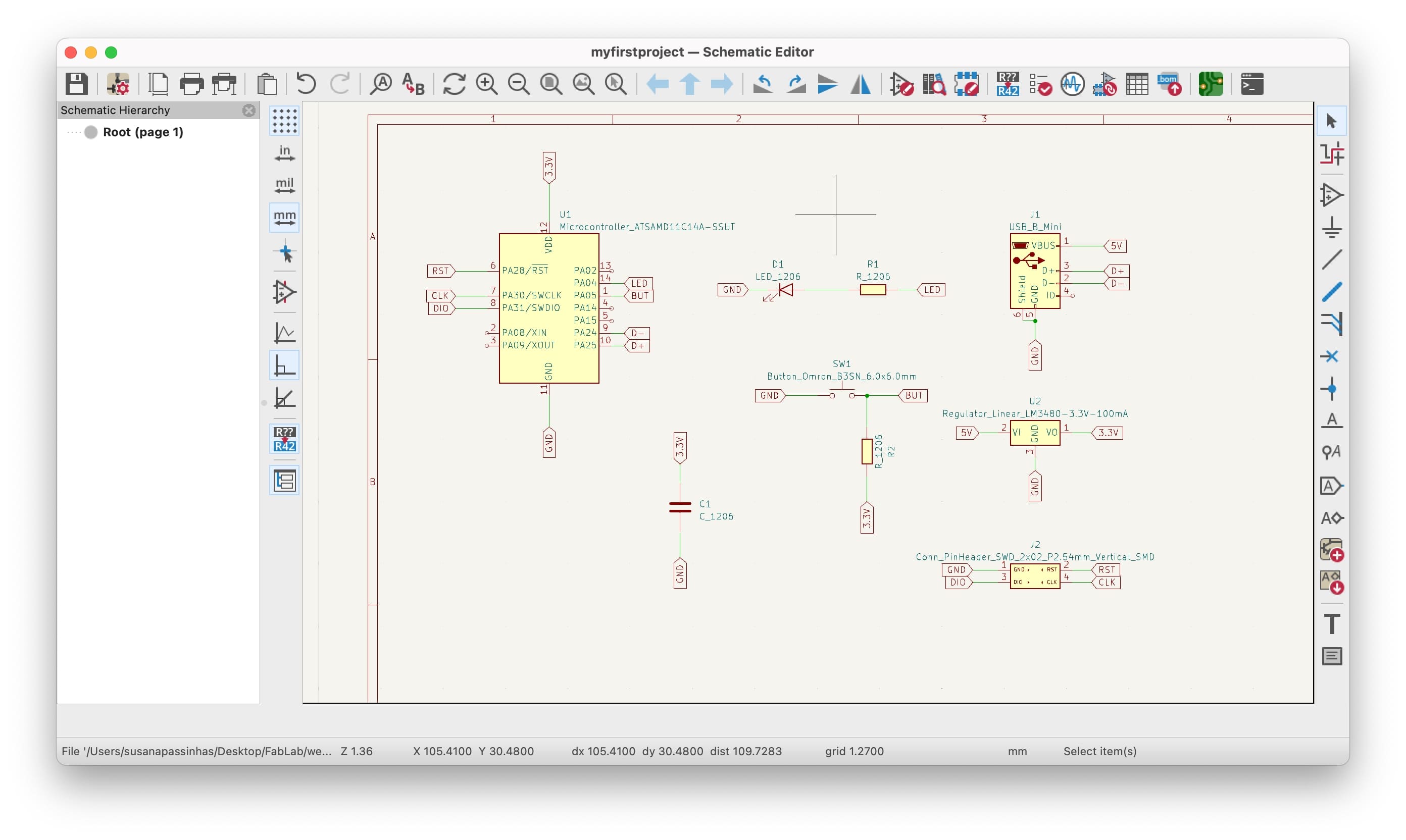
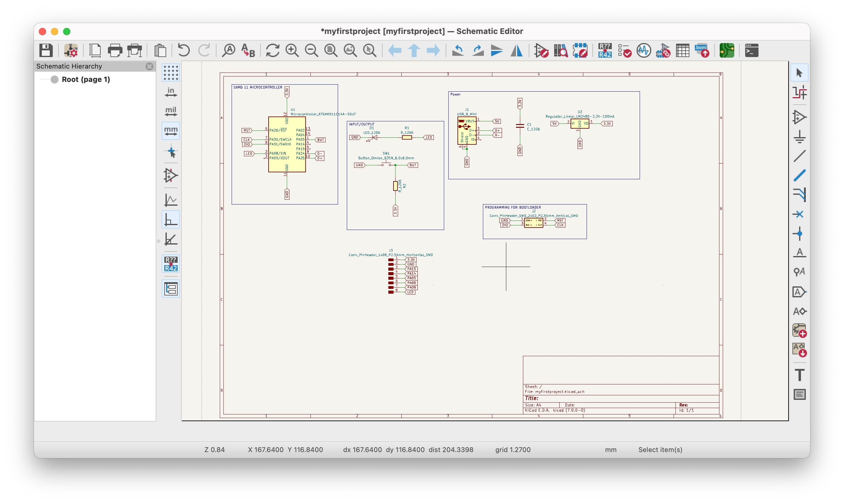
Once the libraries were set, it was time to start adding the components to the Schematic Editor. I created a new project in my computer and started to add the components.
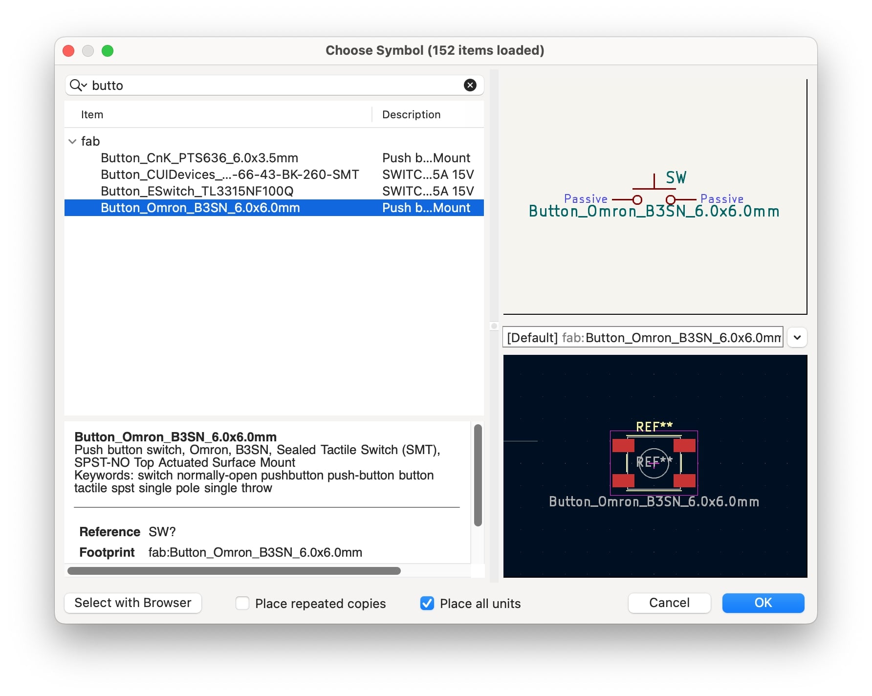
The first component I added to create a circuit was the SAMD 11, we can add components to the schematic simply by clicking on the schematic or we go to the top menu and choose place > add symbol. We can in this view also double-check if the symbol has a correspondent footprint (in the image below). It's important to notice that the pins in the symbol might not be positioned exactly as in the datasheet of the component, this is just to make our life easy when it comes to linking things here.
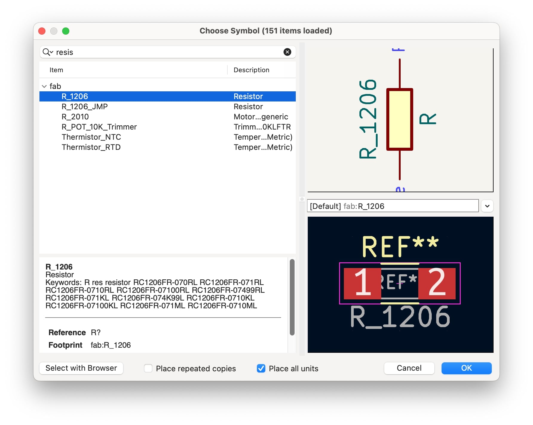
Adding components - Resistor
Now that SAMD 11 was in the schematic I needed to add the other components that will allow me to create an electric circuit that works. So the next component I added was a resistor. A resistor will allow reducing the current flow so that when the circuit goes to ground the voltage is 0V. It's important to notice that in electrical circuits like the one we are doing, we work with DC (direct current) and typically with 5V. Also all the components I added were 1206 - this is the size of the packaging we are using.
To calculate which resistor to use: resistor calculator.
Adding the remaining components - Button, LED, Mini USB and a Capacitor
Then it was time to add a button, a LED, and a Mini USB (Conn_USB_Plain) to connect with SAMD 11 so that we can program the board and a capacitor (C_1206). The capacitor stores electrical energy in an electrical field, it helps balance the current.
Adding labels to components
Once all the components were arranged in the schematic it was time to label them so that I can later create the circuit. Basicaly using lables allow us to identify which elements are the same so we pass the circuit through the elements that do the same, for example all GND (ground) can be connected in the same circuit and all 5V and so on.
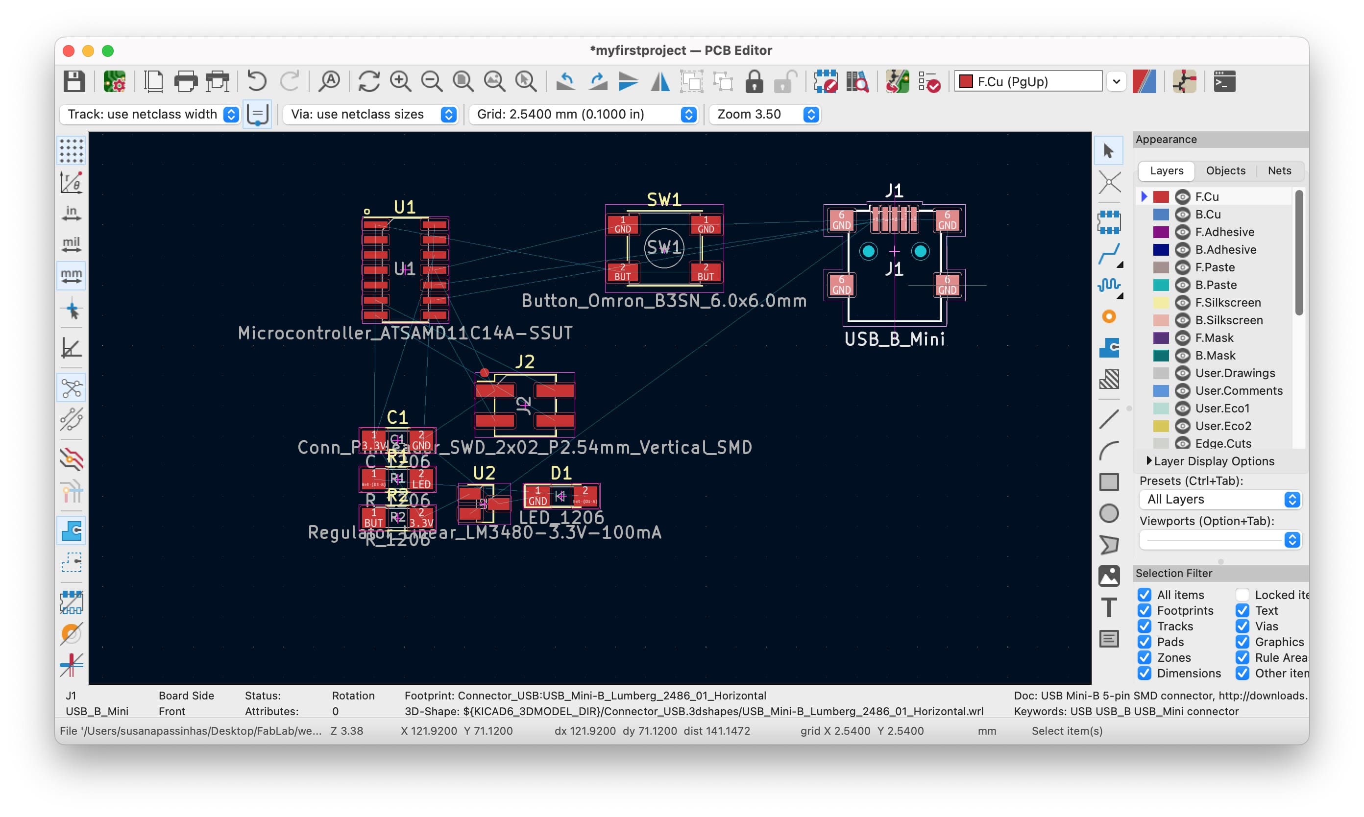
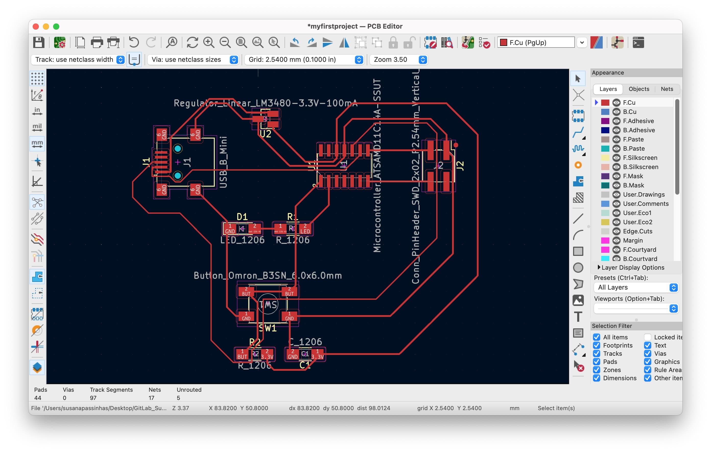
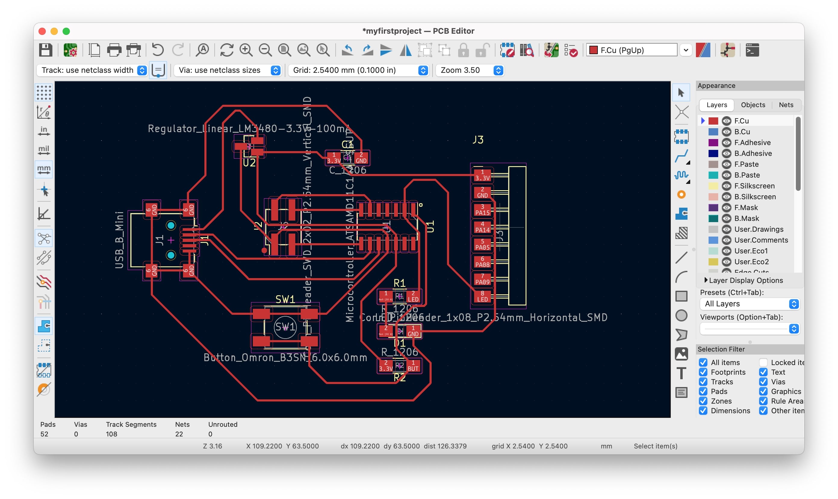
Moving to the PCB editor
In the PCB editor, we can add the schematic components we defined earlier by clicking F8 (update PCB with changes made to schematic) or using the correspondent menu item on the top. Once they are placed I move them around to see the connections I would be needing to make.
Defining the circuit thickness
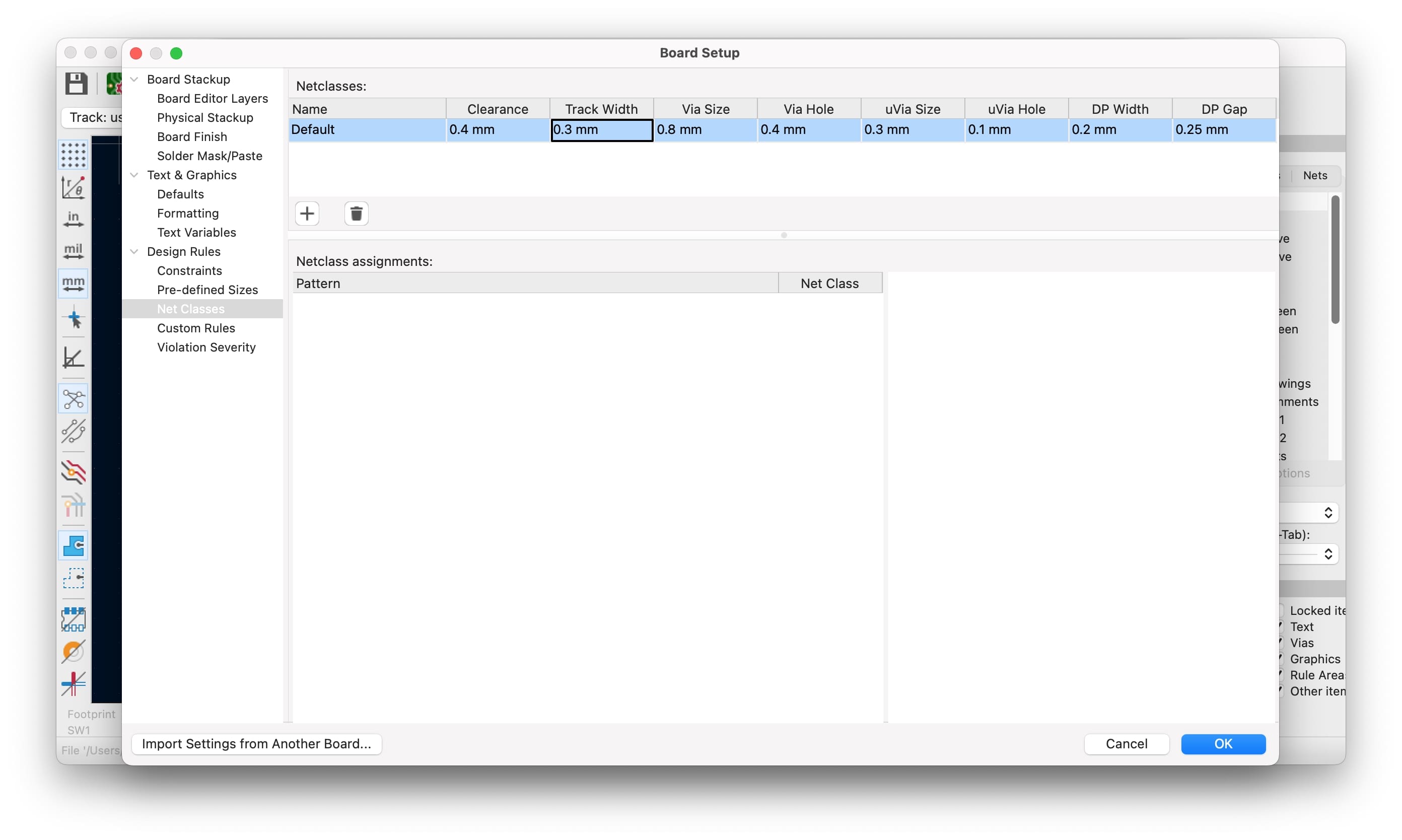
Before starting to create the circuit, I defined its thickness of it (0,3mm) and also the clearance (0,4mm). The thickness refers to the thickness of the soldering and the clearance refers to the space between the lines of the circuit so they don't touch each other. This is important because we also need to make sure our hands and soldering wire have enough space to create this circuit.
Drawing the circuit
I though this would be really straight forward, but it actually wasn't! This is an incredibly complex web of connections and can be quite overwhelming for those who are just starting. I did try a couple of times moving things around, rotating, and so on, and it was really a struggle. I needed to make sure I could pass the circuit through all of the elements with the same label and this was 99% of the time conflicting.
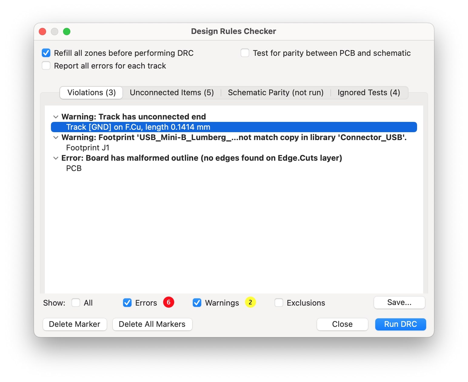
Errors and warnings...
I kept getting errors and warnings in my connections...and I clicked one by one and tried to solve it.
Getting right (almost)
After a few hours of trying I looked back to the class tutorial and re-organized my components and then it was easier to make the connections. I guess we need to have a holistic approach when it comes to organizing things to check what's the best option to connect them all. I feel this is the type of work that will improve with the practice for sure.
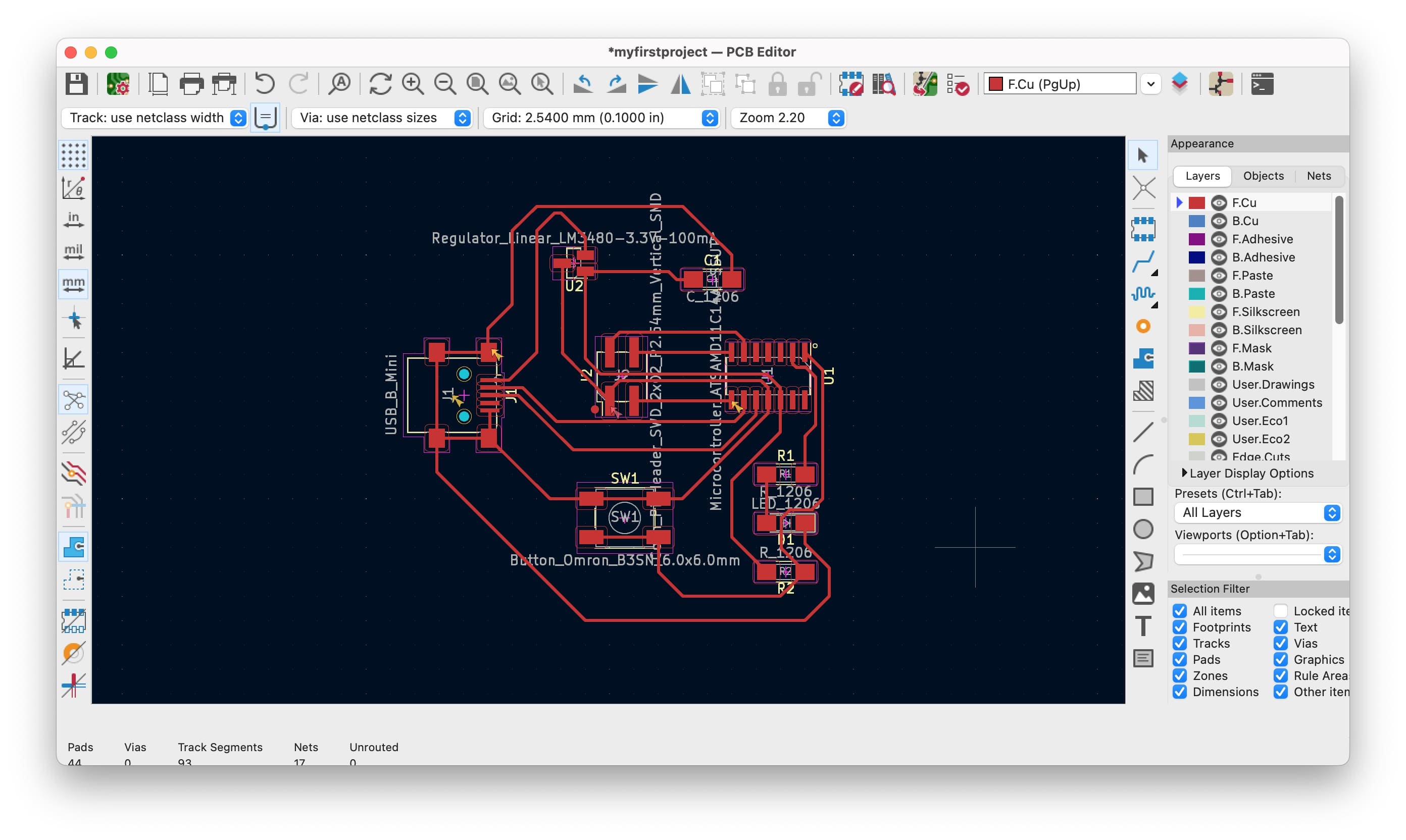
Adding exposed pins
In the end I was missing the exposed pins, so to do that I went back to the schematic editor and added the Conn_PinHeader_1x08_P2.54mm_Vertical_THT_D1.4mm.
I added the labels so that they connect with the right component elements and went ahead and updated my PCB Editor.
Later, during the electronics production week, I ended up realizing I didn't connect all the pins... at the end, I ended up re-designing this board and you can see that process and documentation here.
Updating the PCB circuit again
In the PCB Editor, I added the connections and did tiny changes to make it work. When I run the design rules checker I have one error that I can't figure out what it is about... "Board has a malformed outline (no edges found on Edge.Cuts layer), will try to figure this out!
→ Electronic design files here
Reflection
The nicest thing about this week was understanding better electricity and how the electrical world works. This is something really different from my expertise and it was very interesting to understand it.
On another hand I didn't expected that connecting the component elements would be so hard! I really struggled with it, definetly a lot of mind mapping that for sure I will get more confortable with experience.
Final project and electronics design application
For my final project I will need to develop a PCB based on the needs of my project. I still want to understand more about inputs and outputs before committing to a specific PCB.