8. Electronics production
Make the development board
This week I built and tested the development board I designed in Week07 to interface and communicate with an embedded microcontroller.
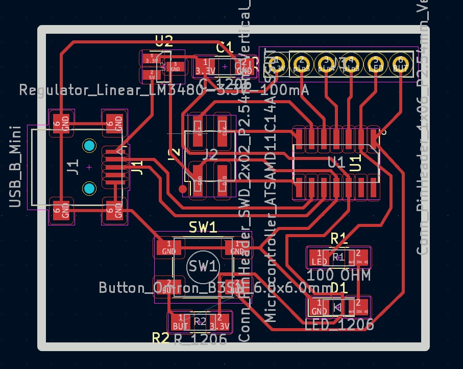
For the preparation of the file, we start from the file that was exported in KiCad in svg format of our circuit. With this file, we are going to work in a CAD program (Inkscape was used) and correctly separate the zones that we want to machine in a different way. In this case, we have 3 differentiable zones: Traces, Holes and Outline.
These 3 zones must finally be 3 different files, since each one will be used to machine different zones with different conditions (parameters and tools).
It is important to be clear that the area to be machined will be the black one. Therefore, in Inkscape, we will work with different layers and we will export what we are interested in each one of them.
To do this, we are going to import the svg format file into Inkscape and create different layers with the names mentioned above. In addition, we are going to create another layer called "Background". Thus, the 3 different layers that will later be exported consist of:
- Traces. It will be all connections for components and routed tracks. They must be exported in white, with black background, because the black color indicates the removal of material in the machining.
- Holes. They will be exported in black, with white background.
- Outline. It will be exported in black, with a white background. This defines the final size of the board.
The main care to be taken in the preparation of the files, besides having to be independent files since they will use different tools and parameters, is to keep the same size and origin to the 3 files. To do this, in Inkscape, you have to preset the size in "export", using the largest size (that of the outline) as the preset size. To do this, we preselect this layer, we give it to custom settings, and already by default are used for all (unless modified).
Thus, we will have 3 files in png format with the same size and resolution.
CAD/CAM preparing
From each of the png files, we can go to https://modsproject.org/ to generate the machine code. Here, we can click on any area of the screen to include a program. Right click on programs --> open program --> Roland - SMR20 mill - PCB. This will be the machine with which I will manufacture my PCB.
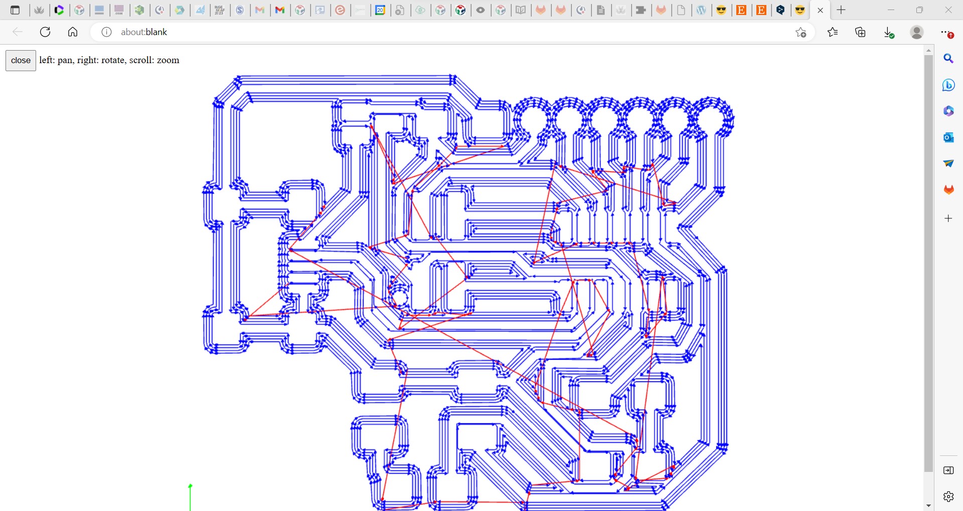
We can insert any SVG or PNG file. In this case, we inserted one of the png images. For this we followed the same order mentioned above, first Traces, then Holes, and finally Outline, to avoid movement or possible vibrations when machining the outer contour.
Here we are shown some default tools, which in turn, have some predefined parameters. The main parameters to be taken into account are shown in the following table. Caution, on the recommendation of our instructors, some of the default parameters have been modified to obtain better results.
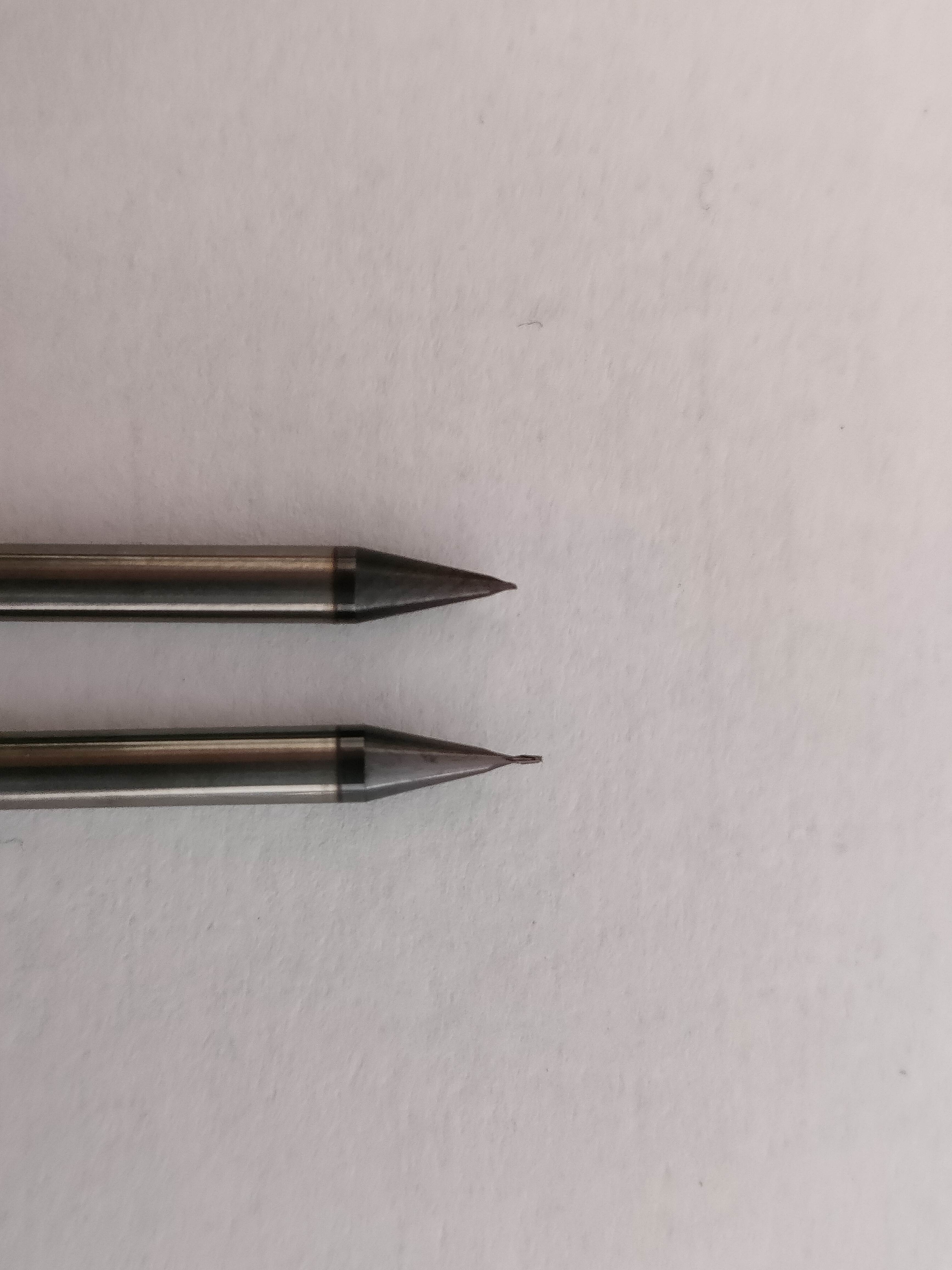
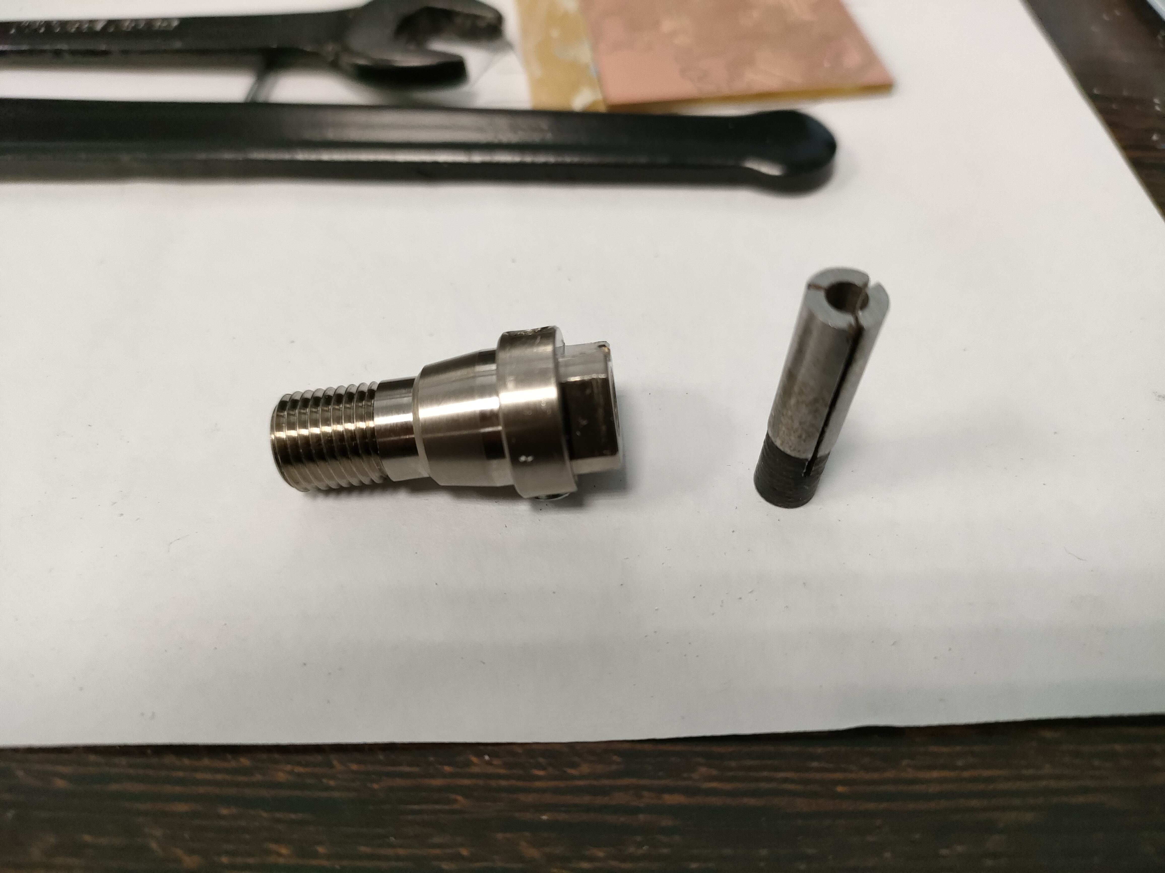
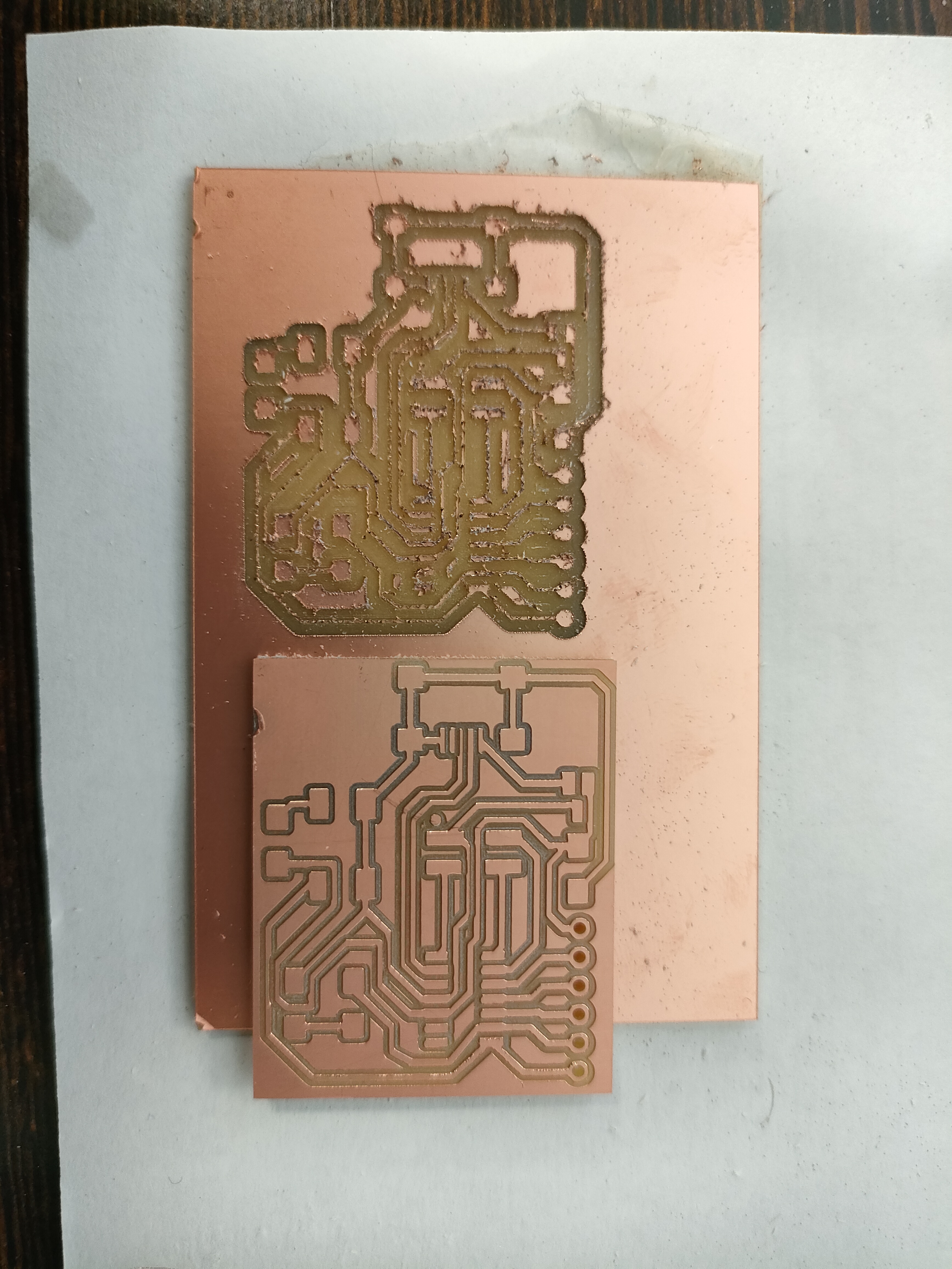
In the first instance, I used the parameters recommended by my instructors, Josep and Edu. However, I had several problems. First, I made the 0 part (in the Z axis) too deep. As a result, when I started to machine the traces, the tool broke. Then, I machined the whole plate, and I had a very bad result (you can see in the picture). This was deduced to be because of the clamping system (also shown in the picture). I think this adapter is less accurate, and may give me some eccentricity with very high stresses and high vibrations.
For the reasons mentioned above and the previous results obtained, it was decided to modify the manufacturing parameters to more restrictive ones, thus lowering the machining speeds. The final manufacturing parameters are shown in the following table.
| Pattern | Tool | Speed [mm/s] | Max depth [mm] | Offset number |
|---|---|---|---|---|
| Traces | 1/64 | 1.5 | 0.08 | 2 |
| Holes | 1/32 | 2 | 1.75 | 1 |
| Outline | 1/32 | 1 | 1.75 | 1 |
The machining direction was climb for all cases. Also be careful with the origin (recommended to put 0 in X Y, but put a higher number in Z, like 60.5 that comes by default), and with the jog height where it is recommended to put a height of at least 2 mm.
Once we have the machining files, we can start with the machine. The first thing to do is to place the tool to be used (for each case) and make sure that the plate to be machined is well fastened to the base. In this case, double-sided tape has been used, since the stresses are not so high as to require a more robust mechanical clamping system. In the video we can see a planing of the surface on which the board to be machined will be placed.
The surface planing can be easily done with the ClickMILL program. All you have to do is select the "surface" technology, define the block size to be machined and the depth. The surface or base support is a block of wax.
Then, we go manually from the VPanel for SRM-20 program to the lower left corner of the plate to make 0 in XY. To make 0 in Z, it is necessary to start the spindle and lower the tool little by little (hundredth of mm by hundredth of mm) until it contacts the plate. We can now launch the surface glide.
Machining
With the surface flat, we stick the board with double-sided tape to the surface. Again we have to make the 0 in the three axes with the new tool (1/64). This time, we have to be more careful with the Z axis because the tool is very thin and delicate (this ill-defined step was the cause of breaking the tool).
From the VPanel for SMR-20 software we can directly launch a cut. By clicking on "Cut" we can include any file (one or several) to be machined and start machining. Be careful not to launch different programs using different tools.
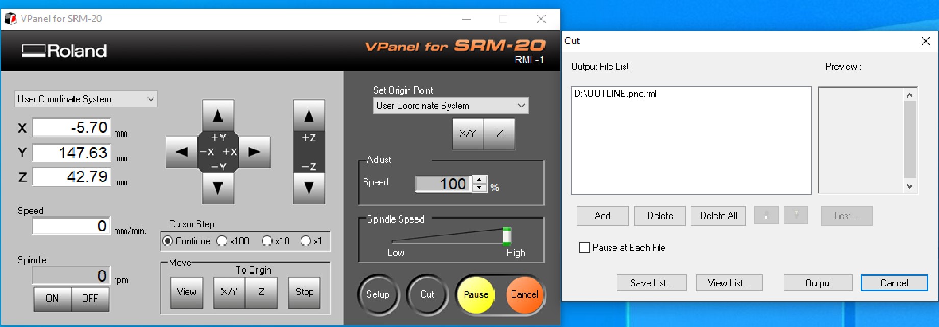
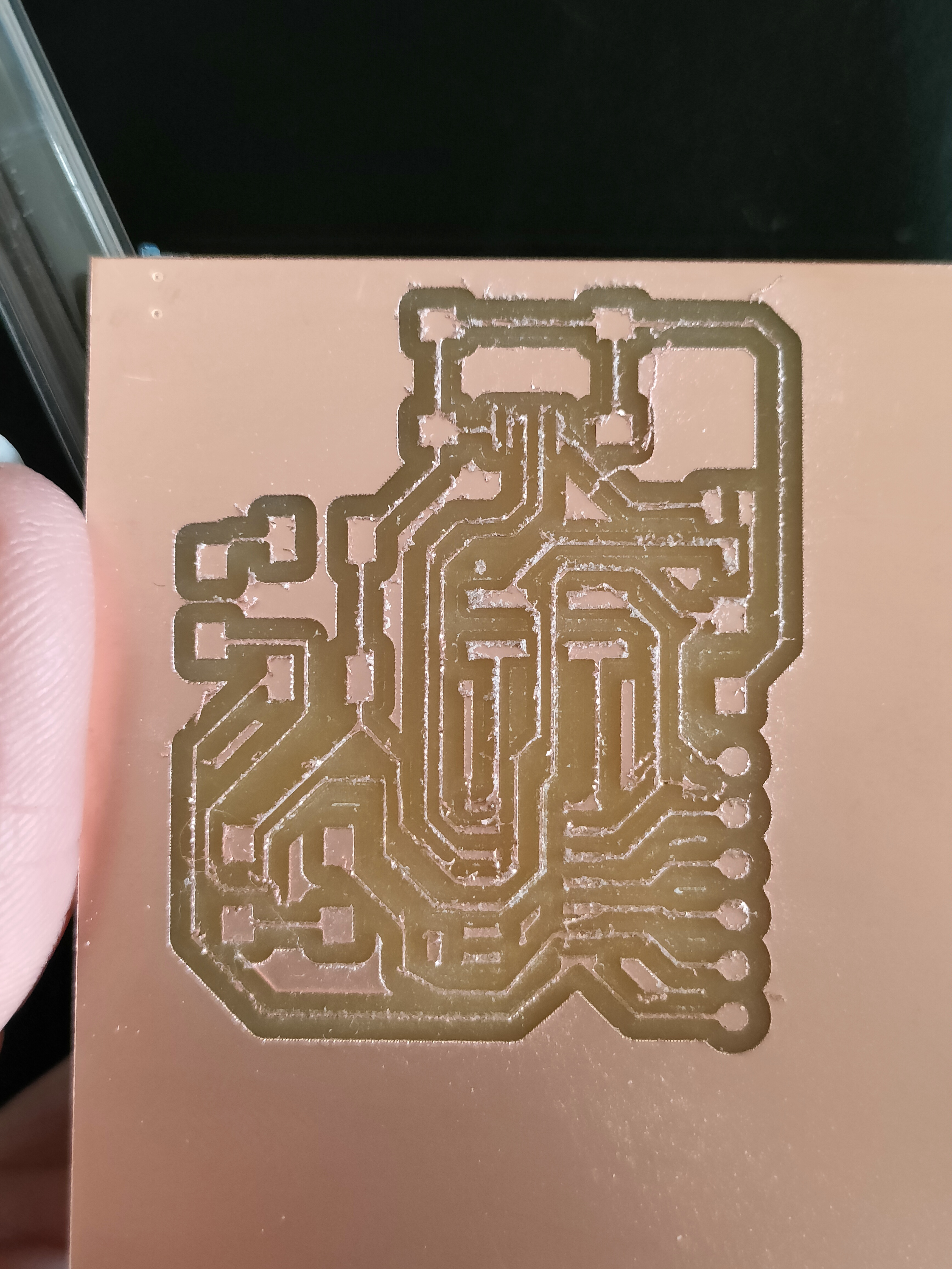
In the following video we can see the slow machining I did. On the right, the image of the result of the well machined plate. (A program has been used to reduce the video size, hence the sign that appears announcing it).
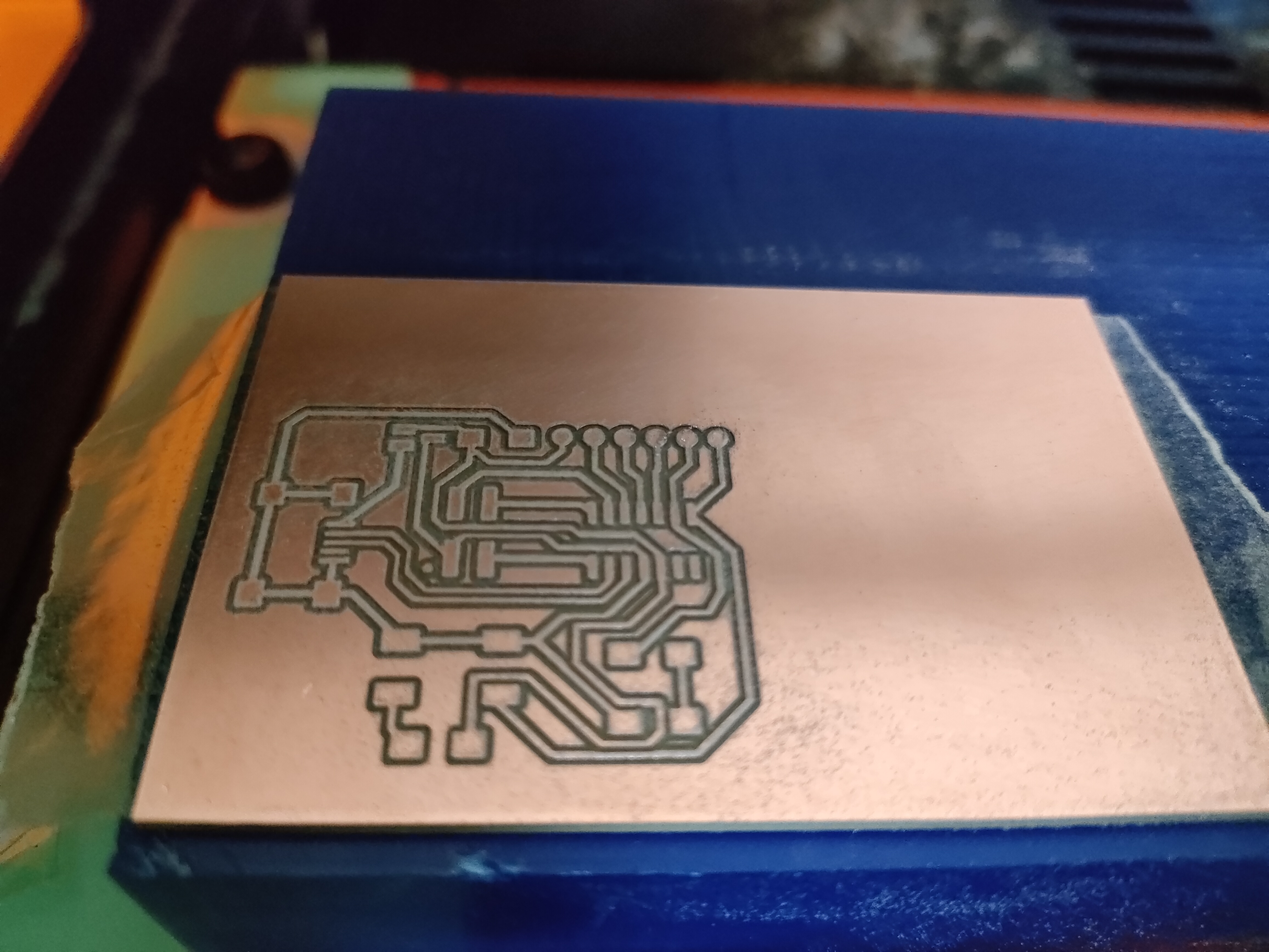
Also in the image we can see the difference between the two machined boards. The first one has a lot of burrs and the paths are almost raised. However, this plate could be used with some external cables (nevertheless, it was decided to repeat it).
Soldering and testing
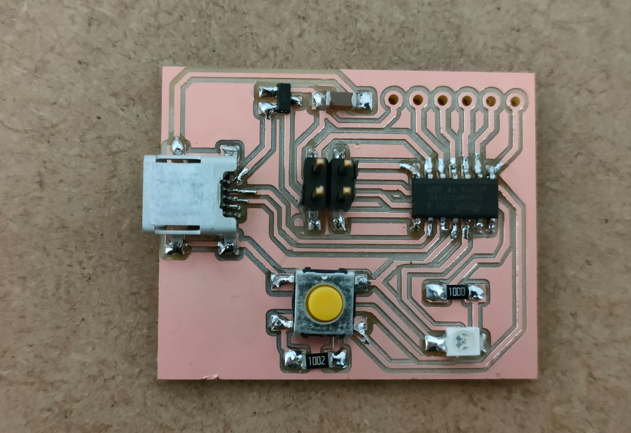
With the board, we only need to solder the components with tin. To do this, we need to have at hand the list of components shown in the following table and the circuit diagram.
The soldering temperature was set at 280ºC. Due to my low soldering experience, I preferred to use a temperature not too high because if I take a little time, I can damage the component or the board.
| Diagram | Component | |
|---|---|---|
 |
USB Mini | |
| Microcontroller | ATSAMD11C14A | |
| Capacitor 1206 | ||
| Regulator | 3.3 V - 100 mA | |
| LED 1206 | ||
| Button | 6x6 mm | |
| Resistor | 10 KΩ | |
| Resistor | 100 Ω | |
The most difficult components for me to solder were the USB mini and the microcontroller, as they are the ones with the smallest and closest connections. For this reason, and recommended by my instructors, these are the components to be soldered in the first place.
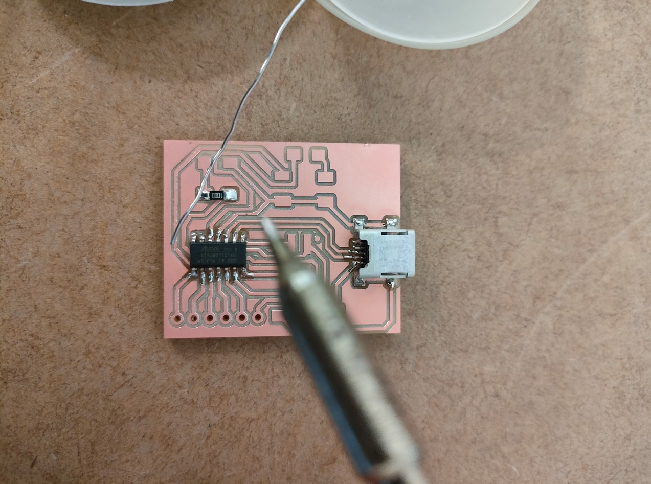
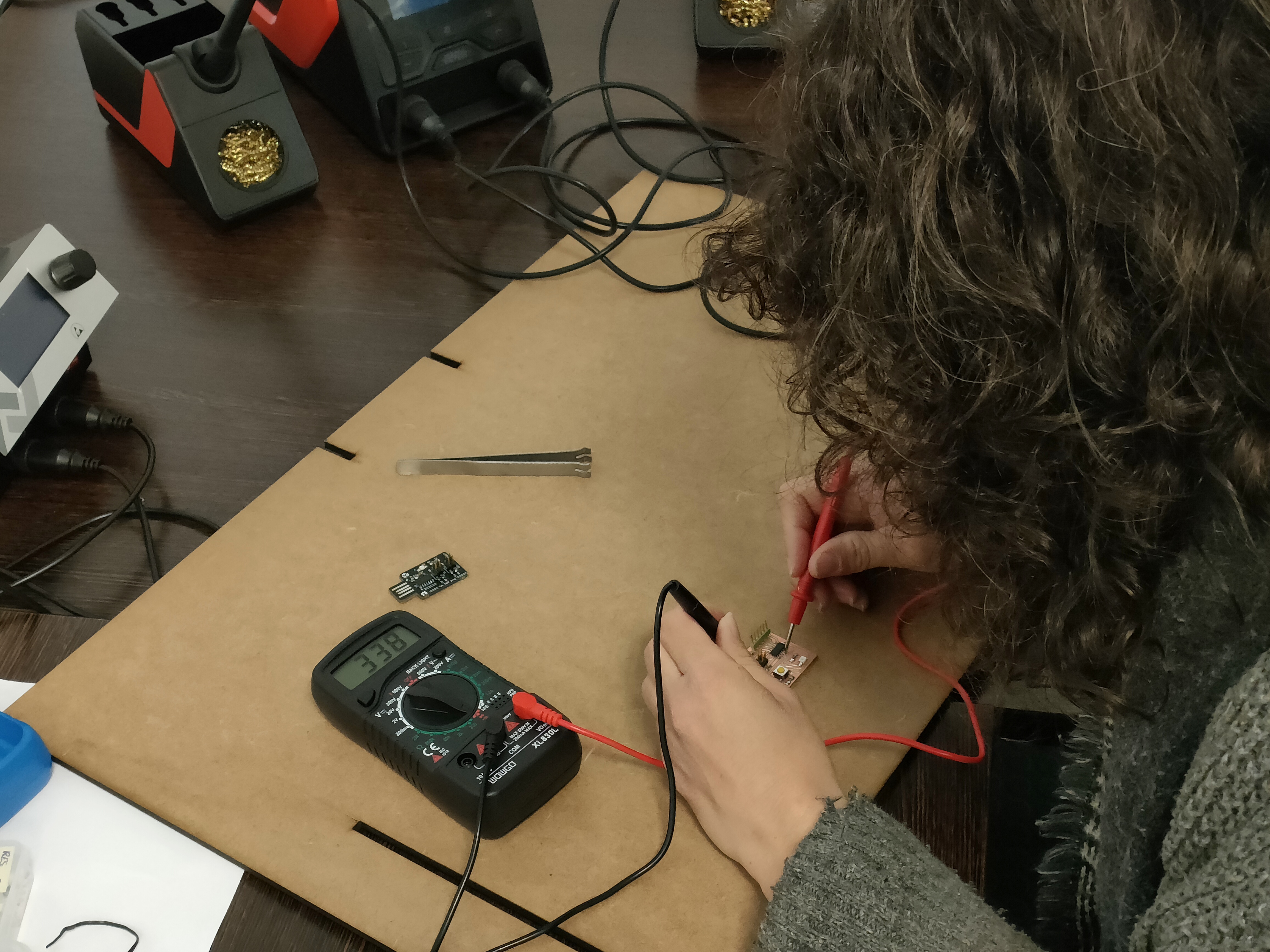
When all components were soldered, the pins were inserted into the holes, and the connections were checked for good connections with the multimeter.
Programming
In order to program the board we need a programmer. So, not only did I fabricate my board, but I had to fabricate a programmer. The one I made was the Programmer SWD D11C (in the link you can find all the information and files about it). The process to make it was the same as for my board.
To program a SWD D11C so that it can act as a bootloader, it must first be programmed with another programmer. In FabLab Barcelona they gave us the same one and I connected both of them.
The code is in the previous page, with all the information and steps we need to follow. So, I downloaded the binary file that will make the board a programmer. Also needed is the edbg file which is a software that allows to program the board. Then I opened the Git terminal and I used the command:
$ ./edbg --help
to see what options I have with this file. With the command we are going to use we can know that we need the "e" to erase, the "b" to tell us what is happening (verbose), the "p" to program and the "v" to verify.
Thus, I was able to program my programmer with the following command:
$ ./edbg -ebpv -t samd11 -f free_dap_d11c_mini.bin
I then checked that I had two programmers with the command:
$ ./edbg -l
Once I had my programmer, I could disconnect the programmer from the FabLab and I can now connect my programmer to my board. In the image you can see how both boards have to be connected.
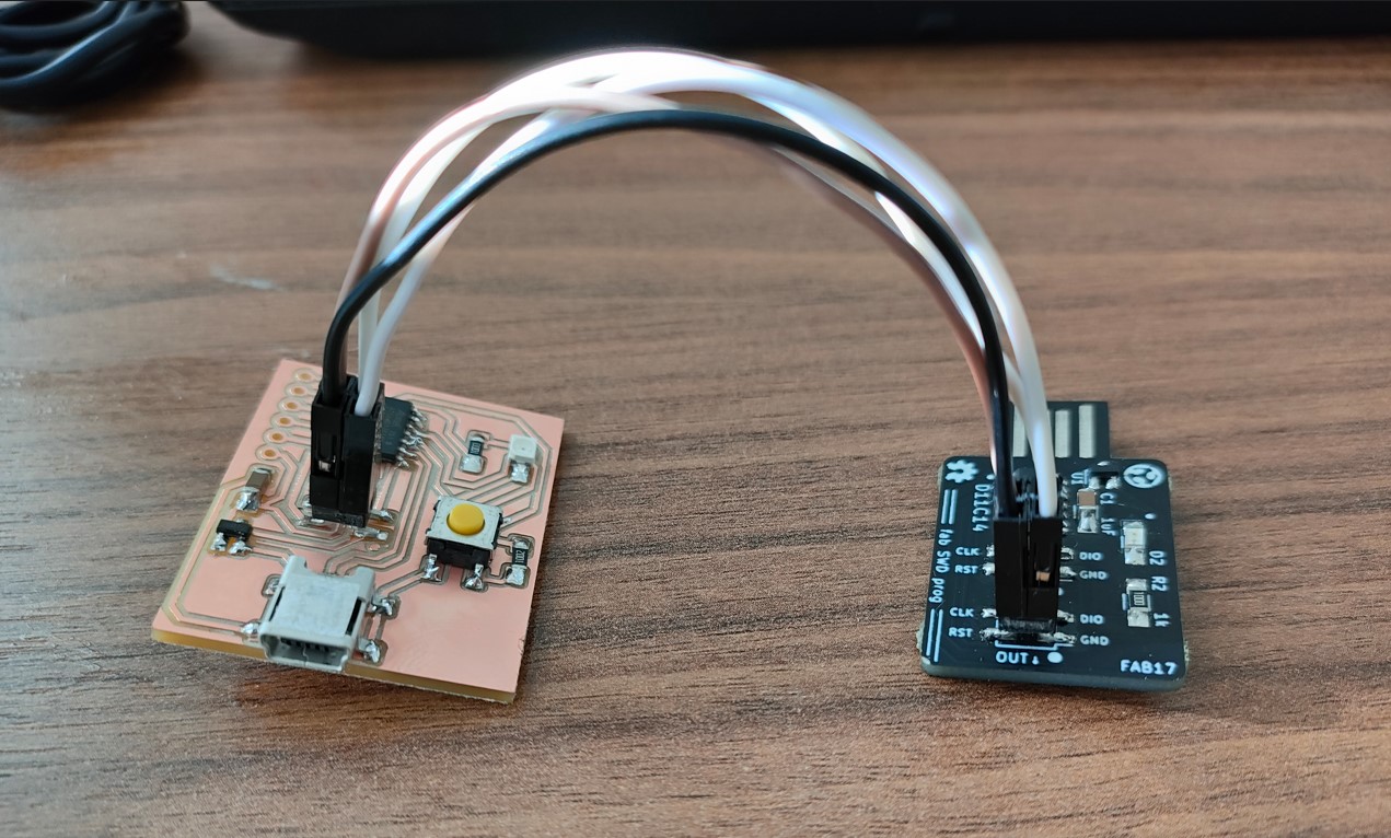
If you look at the picture, with the connectors in the same position (the dot indicates the ground), you have to connect the wires in the same order. It does not matter the orientation of the board, but the orientation of the connector.
Now I only have to flash the bootloader onto the target board with the comand:
$ ./edbg -ebpv -t samd11 -f sam_ba_SAMD11C14A.bin
With the board preprogrammed we will only have to check that it is OK from the Arduino panel, with some of the simplest examples it has will be enough. So, I used a simple program to turn on and off the LED with the button on my board, programming pins 1 and 2.
  	const int buttonPin = 5;
	const int ledPi = 8;

	int buttonState = 0;

	void setup() {
  	  pinMode(ledPin, OUTPUT);
  	  pinMode(buttonPin, INPUT);
		}

	void loop() {
  	buttonState = digitalRead(1);
 	 if (buttonState == HIGH) {
        digitalWrite(ledPin, HIGH);
  	} else {
        digitalWrite(ledPin, LOW);
  		}
	}
Files
The traces file.
The holes file.
The outline file.
Group assigment
The group assigment can be viewed at Group Assigment page.
Conclusions
To carry out machining, especially with small and precise tools, you can't be in a hurry. Any wrong step (e.g. making the wrong 0 in Z, or incorrectly positioning the tool or the workpiece) can render useless what we are doing, break the tool and ultimately waste more time.
On the other hand, soldering such small components is no easy task. You need peace of mind, good light and a good pulse. In my case, I didn't have to make big changes because I had practiced a lot with my instructors previously. They showed me how to check that the soldering is correct and how to remove excess solder or even remove misplaced components.
Finally, programming. It is the task that is the hardest for me, maybe because I find it more difficult or I still don't understand it enough. It is necessary to continue practicing...