6. Electronics design
This week we worked on electronic design. First, the instructors of Fab Lab Barcelona gave us notions of electricity, to better understand and know how to design with criteria. In my case, despite being an engineer, my knowledge of electricity and electronics is very limited, so these sessions were very useful for me.
Electronic design is the design of a circuit, knowing how it works so that we can then produce it on a PCB (printed circuit board).
Individual assigment
I designed a development board to interact and communicate with an embedded microcontroller. For this, I used a SAMD 11 microcontroller. This is one of the microcontrollers used in Fab Lab Barcelona (on the Barduino board studied in week 4) that allows us to communicate via USB.
To create a PCB (printed board circuit) design there are different programs. Some of the best known are listed in the following table:
| Software | Advantage / disadvantage |
|---|---|
| Altium Designer | Intuitive, integrated with CAD software (solidworks, autodesk,...). For a fee. |
| Fusion 360 | Integrated CAD and CAM. For a fee. |
| Siemens PCBflow | Detailed error reports. For a fee. |
| DipTrace | Intuitive interface. Short library. For a fee. |
| Ultiboard | Advanced design assistant. For a fee. |
| OrCAD | Simple. Free. |
| KiCAD EDA | Open source. Extensive official library and possibility to design new symbols. Free. |
PCB design software can help us design our printed circuit boards easily and efficiently, while saving a lot of time and resources. It will also help us verify the performance of our design and correct it in the early stages so that you can send only high-quality designs to the production stages. As a result, I can manufacture solid, reliable printed circuit boards that work well in electrical devices. We have used the KiCAD software.
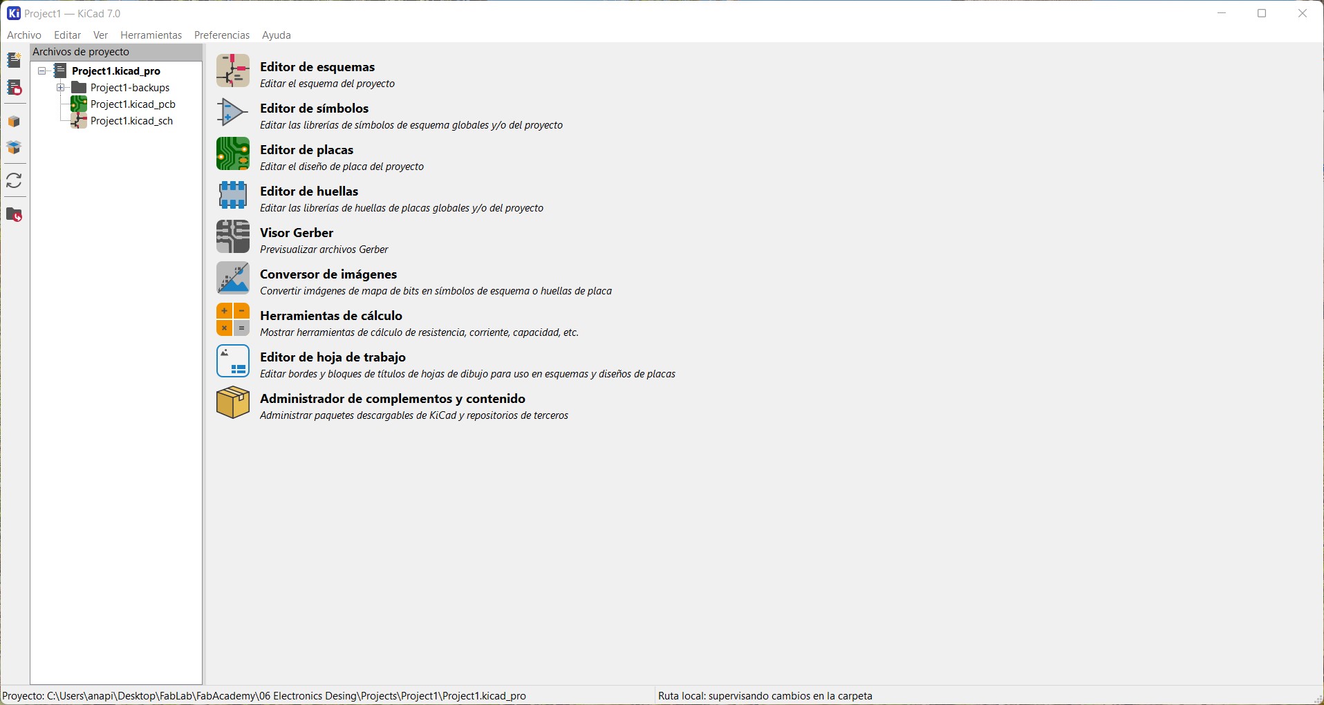
PCB design
KiCad is quite easy and intuitive. In it, I generated a project that contemplates both the schematic editor (where you add all the components) and the PCB editor (where you connect the components).
The basic steps for creating a development board that can communicate are outlined below and explained later:
- Create a project
- Generate the schematic, adding all the elements I need
- Place labels and organize the schematic view
- Modify values as needed
- Generate the PCB editor and place the components
- Edit the predefined sizes (in track)
- Arrange components and readjust
- Join components
- Test using DRC
To know what components we need and how they go together, we need to have some knowledge of electricity and electronics. For example, we need to know that some elements have polarity (such as LEDs) and others do not (such as resistors).
First of all, we add the libraries of the components that are usually used in Fab Lab Barcelona, since KiCad, although it contains an extensive library or catalog by default, does not contain the specific microcontrollers of our Fab Lab. These libraries are in GitLab, so we can clone them in the computer and then insert them in KiCad. To insert them in KiCad we have to open in the program the preferences -> manage library of symbols and/or footprints and add them from our repository.
Within the schematic editor, it is very easy to import components. We simply use the command ![]() command and search in the library for the components we want to import.
command and search in the library for the components we want to import.
Once we have all the desired components, we must add a label with the command ![]() . The labels will designate the component to be joined.This step is very important, otherwise we will not be able to join the terminals in the PCB editor.
. The labels will designate the component to be joined.This step is very important, otherwise we will not be able to join the terminals in the PCB editor.
One recommendation from our instructors is that we put together the components that make up a unit in a chart. For example, the "power" unit will consist of the USB, a capacitor and a linear power regulator. Another example could be to associate an input with its output. To create a box and to be able to put a text we can use the commands ![]() and
and ![]() respectively.
respectively.
In the picture we can see all the components inserted in my board (schematic) and organized in boxes with labels.
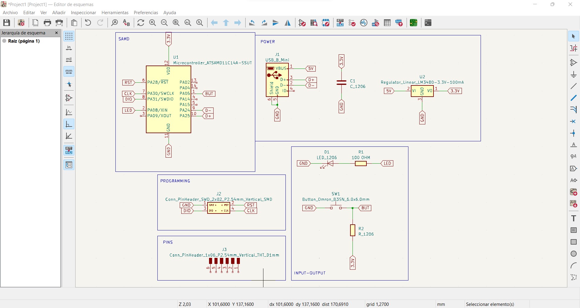
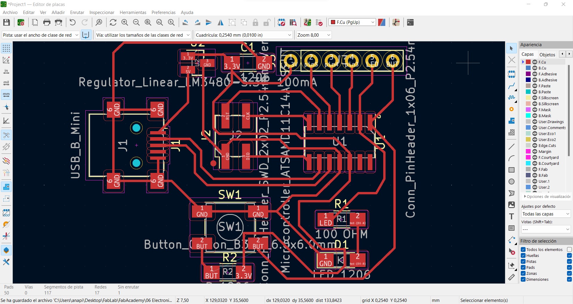
We can now open the board editor. In it, we can place and rotate each of the components as we wish, to occupy as little space as possible. We have to pay attention to the blue lines because they show us the connections that we have to make and can give us an idea of the most favorable orientation for the components of our circuit.
Once we have all the desired orientations, we must route tracks with the command ![]() .
.
Actually, we must first check that no sketcher of the elements is stepped on, and that the tracks are large enough to be able to perform them with our machining tool later. If this is not taken into account, the paths generated in this program may not be respected in the machining software.
For this, in network classes, we can edit the margins or edges from one path to another, the track width, the hole diameters, etc. In Fab Lab Barcelona we use a 1/16 tool for the tracks and 1/8 for the machining of edges and holes. Thus, the parameters used in the software are reflected in the following table:
| Parameter | Margin | Track width | Track diameter | Track hole | Track size |
|---|---|---|---|---|---|
| Value | 0.4 mm | 0.3 mm | 0.8 mm | 0.4 mm | 0.3 mm |
In my case, I did not put labels on the pin at the beginning, because depending on the board, it will be more or less comfortable to associate the pins to one element or another. This generated me an error, since directly in the board editor, I could not link those pins. I had to go back to the schematic editor, add the labels and update the PCB editor with the command ![]() .
.
Finally, the designed board can be seen in the following image.
Once finished, we can check for malfunctions with the command ![]() . That is, do a design rules check (DRC). With this we will be able to check elements that are not connected, or tracks that are stepped on and thus modify them so that they work correctly.
. That is, do a design rules check (DRC). With this we will be able to check elements that are not connected, or tracks that are stepped on and thus modify them so that they work correctly.
Once the DRC analysis was done, I obtained the main errors:
- Screen printing overlap. Here it is important to be clear about what we are going to include in the plate to be manufactured, and what is going to be used only in the scheme. If we want to export the silkscreen (this is not the case), we must avoid overlapping with the components and paths.
- The USB footprint does not match the library footprint. This is because we have modified the connectors so that we can make them with our tool and check that they do not overlap.
- The board has a malformed contour. We have not defined the contour or outer edge of the plate for machining. This can be done by drawing the outline as a layer, or we can even draw it in another program (recommended by our instructor, especially if we are going to make special shapes or we are going to make the USB adapter with the necessary shape and measurements).
Group assigment
The group assigment is available at the following link: GroupAssigment
Files
The files for 3D printing are included in the following link.
Conclusions
This week it has become clear to me that I cannot design a board without a good understanding of the concepts of electricity and electronics, to know how the components go together, so I have a long learning curve ahead of me.
On the other hand, once you know the components and the connections between them, the KiCad software is very intuitive and easy to use.
However, the joining of components is more difficult than I expected, because you have to take into account that they cannot overlap. Also keep in mind that we must not make paths with right angles, as they give resistance to the circuit.
In short, it is important to know and know how to design PCBs to be able to adapt them to the needs of a specific project. I have thought about my work and many doubts arise, especially with the outputs that I need or might need and the programming linked to this board.