Week 6. Electronics Design
Before the Start
Introduction 🖊
This week relates to Electronics Design! Circuits, Voltage, Current, Resistors, Capacitors, … We’ll learn the basics about the Art of electronics, design our own “Hello World” PCB board, fabricate it, and try it out!
Fab Assignments 📚
-
Group assignment:
- Use the test equipment in your lab to observe the operation of a microcontroller circuit board (in minimum, check operating voltage on the board with multimeter or voltmeter and use oscilloscope to check noise of operating voltage and interpret a data signal)
- Document your work to the group work page and reflect on your individual page what you learned
-
Individual assignment:
- Redraw one of the echo hello-world boards or something equivalent, add (at least) a button and LED (with current-limiting resistor) or equivalent input and output, check the design rules, make it, test it. Optionally, simulate its operation.
My Goals 🎯
- What I think I already know
- I have theory knowledge about electronics, but I never designed my own board. Thanks to the experience acquired two weeks ago, I also already know how to mill and solder the components in a board.
- What I want to learn
- Deep research about the topic, especially watching the recommended youtube electronics channels.
- I want to design a workable board.
- Get the experience needed to be able to use all this info to start defining my final project’s board, also use this knowledge for my next personal projects.
Project Management
| Task | Time | Day |
|---|---|---|
| Research | 6h | 3 / 4 March |
| Group Assignment | 6h | 3, March |
| PCBs Kicad Design | 10h | 4 / 5 March |
| Milling | 3h | 7 March |
| Soldering | 3h | 7, March |
| Programming and testing | 3h | 8, March |
| Documentation | 8h | 4 / 5 / 7 / 8 March |
Files 📂
| Name | Description | Link |
|---|---|---|
| File 0 | Hello World Board 1 - Traces | File |
| File 1 | Hello World Board 1 - Outlines | File |
| File 2 | Hello World Board 2 - Traces | File |
| File 3 | Hello World Board 2 - Outlines | File |
Research
Since I’m new with electronics design, I decided to use a big % of the week’s time researching more in deep about PCBs, KiCad, components, in order to feel sure that I have the previous knowledge to design my own PCB!
I principally watched the videos from these two Youtube channels:
During the Process
Group Assignment Process 🏊♀️ 🏊🏾 🏊🏽♀️
Erwin’s Introduction to Electronics design
We started the week with a marvelous theory introduction for electronics design by Erwin.

He explained to us the basic concepts about electronics design, the meaning of PCBs, the components needed to build them up, and the measuring tools in use to check the current, voltage, etc.
Attached is a re-cup of all the concepts which he explained during the class.
If you want to know more about electronics design, Erwin also recommended us this book:The Art of Electronics
Basic concepts
| Name / unit | Meaning | Formula |
|---|---|---|
| System | Groups of electrical components connected to carry out some operation | Input > System > Output |
| Circuit | A circuit is a closed loop where electrons can flow | — |
| Voltage (V, Volt) | Difference in electrical potential between points. The sum of all voltages around a loop = 0 | V=P/I |
| Current (I, Ampere) | Amount of flowing electrons. The sum of all currents in a node = 0 | I=P/V |
| Power (P, Watt) | A measure of how quickly it converts energy | P=V*I |
Components
| Name / unit | Meaning | Formula |
|---|---|---|
| Resistor (R, Ω, Ohm) | A resistance for electrons | R=V/I |
| Capacitor (C, Farad) | A storage tank for electric fields (charge) | C = Q/V , I = C dV/dt |
| Diode / LED (D) | One-way valve for electrons. Often used as bridge rectifier | — |
| Coil (L, Henry) | A storage tank for magnetic fields | L = V / dI/dt |
| Transistor (Q) | Amplifier and/or switch | Ic = β * Ib where β = amplification factor |
| Microcontroller (U, IC) | Integrated Circuit, built from transistors. Programmable device with inputs, outputs, memory and calculation engine (ALU) | — |
Measuring
| Name | Measures |
|---|---|
| Multimeter | Voltage / Current / Resistance / more… |
| Oscilloscope | Multiple voltage in time domain / Frequency counter |
Testing the measuring equipment
After Erwin’s introduction to electronics design, we tried out some measuring tools in PCB boards that we had in the lab.

I tried all the measuring machines, starting with the Tiny Red Multimeter that we have in the lab. With it,
I measured:
- Resistances: trying to predict their measure by calculating the resistance sum with their lines color legend.
- Voltage in a PCB circuit:
- From the + power pin to the C1 capacitor.
- From one side to the other of the Transistor.
- From the Microcontroller to the Resistances.
- From one side to the other in a LED.

I also tried out the Digital Tweezers, with them I measure some resistances like I did with the Multimeter.
Finally I tried out the Oscilloscope
With the Oscilloscope I compared different Voltages in 2 parts of the PCB.

Individual Assignment Process 🏊♀️
This has been the week where I did the most mistakes since the Fab Academy started!
In fact, I had to re-make my board because I missed out and located wrong some components … Spoiler.
Getting started with KiCad
In order to design my PCB board, firstly I watched different videos from the DigiKey channel and also this handy video by the Aalto Fablab.
First round
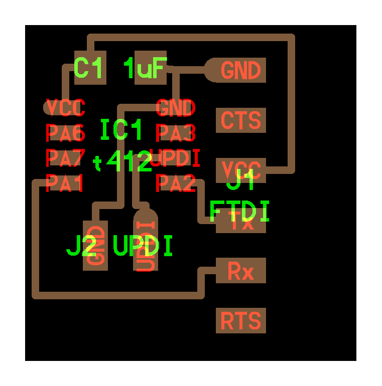
I decided to use the ATiny 412-echo board as a starting point. Then I added the LED and Button component which the Individual Assignment required!
Once I did a list of all the components I needed for my board, I followed this steps to design it with Kicad:
-
Open a new file in KiCad and call it: hello-world-t412. Then located it in a fab folder to have track of it. This is an important step if you want to work in an orderly way.
-
Open the Schematic layout manager:

- Select symbolic components:
Add to the board all the basic components that you need. Tap on the Add symbol option on the right menu, a window will open. Start tapping “Fab” in the library searcher to easier find each component:
- fab attiny 412: microcontroller
- fab updi
- fab ftdi
- fab unpolarized capacitor
- fab resistor
Till now I added all the components from the tiny 412 board, now I will add the extra components for the individual assignment:
- LED
- Button
- power flag 1
- power flag 2
- photocontroller

During this step I did not have any problem looking for the components and putting everything down in the scheme.
- Connect components together by wires:
Next step is to draw the wires between components. Tap “W” where you want to start a wire. I draw the wires to be able to add the layers in the next step. In order to do it, I checked this link to the ATiny componets scheme.
- Annotate layers / components:
If you ever worked before with Illustrator, understanding the KiCad layers is very easy to do. They determine the parts and fabrication process needed to make a PCB. Since we use 1 layer Cu plates at the FabAcademy, we need to use 2 layers in our draw:
- B.Cu layer: for the traces
- Edge Cuts: for the outlines
In this way, when we will save our draw, we will be able to save two different files for each part of our PCB.
In order to add layers to your board, you need to tap “l” and a layer menu will show up. In this menu you can write the layer’s name, choose the text’s orientation, and personalize the text font, size, etc.

Here I did a few mistakes when locating the layers that I discovered when adding the traces to my board :'(
- Run Electrical Rules Checker:
Once all the layers are located, its needed to double-check that everything is well connected. In order to do that, run a DRC test on your schematic.

Here I had a few mistakes because I did not fill in the scheme all the symbols reference designation before running the DRC test. In fact, when adding the components, if there are for example two resistance, they both will be named as “R(?)”, so when running the electrical test, KiCad reads two components with the same name and it gives errors. In order to solve the error, I had to press the symbol on the header named: Annotate Schematic. In this way, KiCad assigns values and footprints to the schematic.
Afterward, I did run again the test and everything was correct. So I could move on to the next step.
- Create a Netlist:
Its important to make this step before opening the PCBnew layout editor. This is the file which will be open to design the board.
My KiCad layout did not had the header option which allows you to export it easily. I fixed this problem looking for the option in my computer header.
In case you have the same problem, this is the path you need to follow:
FILE > EXPORT > NETLIST
Save the .NET file in the same folder where you have the Kicad layouts of your design.
- Open the PCBnew layout editor:
Here is where you basicly design your board. Once you have added all the components and layers to your schematic manager layout. Open the .net file in this new Kicad window.
Before the start, its needed to change some parameters in the Board Setup.
Change the following parameters at the DESIGN RULES > CONSTRAINS
| Parameter | Number |
|---|---|
| Minimun Track Width | 0.39 |
Change the following parameters at the DESIGN RULES > NET CLASSES
| Parameter | Number |
|---|---|
| Clearance | 0.4 |
| Track Width | 0.39 |
- Locate and orientate the PCB components:
Following the instructions from the youtube channels I watched, I tried to place the physical components of my first board making sure that the white lines of the connections were not overlapping each other.
I then discovered that I wrongly connected them since the UPDI and FTDI needed to have the pins looking to the outside and not to the inside like I did :,(
Tip: always locate the capacitor close to the Microcontroller in order to make sure that is protected.
add components orientation.
- Connect components by traces:
Tip: Start connecting the important components, and end connecting the components to the ground.
When adding the traces to my first board, I had a problem regarding the layers nomenclature. Since I named the button connection in two ways (“BTN” and “BUTTON”), KiCad was not letting me make the traces between the Microcontroller and the Button.

In order to solve this problem, I had to update the names in the scheme layout and then upload the changes in the PCB layout.
- Draw the outline:
Move to the Edge.Cuts layer and draw the outlines of the board.
In my case, I decided to draw an outline with the shape of a skull, since when I located the components in the board it tough it looked like it. Yeah, I’m the kind of person who likes to see elephants in the clouds!

When running the DCR test, I had an error with the connection of the outlines. The error happened because the end point of two lines were not centered, I had to center them and then the problem was solved.
- Add ground connections:
This step follows the previous one because we need an outline to make board-ground connections.
In order to do it, add a Filled zone area in the perimeter of the PCB outline. In my case, since I have a skull shape, I did a rectangle design, ensuring that the full area of my board was within the perimeter.
Once te filled zone is done, you will need to fill the zones using the following path to ensure that the ground connections are visible:
EDIT > FILL ALL ZONES

-
Export your design as an .SVG, considering the following options in the export menu:
- Copper layers -> F.Cu
- Technical layers -> Edge.Cuts
- Print Mode -> Black and White
- SVG Page Size -> Board area only
- Print one page per layer -> in this way 2 different .SVG files will be save, one for the traces and another one for the outlines.
-
Modify the outlines file:
When using mods to mill the board, will be needed to modify the outlines file. In fact, the program does not read the outline draw correctly.
In order to fix the problem, open the outline file with Illustrator / Inskcape. Make a black background and convert the outline into an white area. Mods will be able to read now the file.

- Mill the PCB:
As we learned during the electronics production week, will be needed to mill in two times the traces and outline of the PCB.
When using mods, I had a problem with the view of the cutting lines (both with the traces and outline), which I fixed increasing to 1000 px the resolution of the view.

- Solder the components in the board:
When soldering the components in my board, I discovered that I did a few mistakes:
- Layers of the microcontroller = the RX and TX were in the positions of the LED and SENSOR.
- c = missing the VCC connection between the phototransistor and the microcontroller, also the connection to the resistance.
- J1 = I used a 2 pin FTDI instead of 3 pins one.

I had then to re-make my board, and this time I dedicated myself to making a different design in order to use less amount of material.
Second round
When redesigning my board, I wanted to make it using the less possible material. This is why, this time I decided to design a less creative board, drawing a rectangle as an outline:


Attached some pics of the production and testing of the new Hello World board which I finished the week after. It worked perfectly in the end! :)

Retrospective 🤔
This week I learned lots about Resilience.
Learning how to use KiCad was a challenge. I did lots of mistakes, but I tried to fix them and actually find solutions to all my problems. I also had problems when milling the board, but I make it finally work. I had to repeat the board in which I put a lot of time and effort. While designing the new board, I felt that I had already done the hardest part of the learning curve. In fact, designing the new board was a piece of cake in comparison with the previous one.
I did not have time to mill, solder, and try my new board because of the lab capacity. I did plan my week to have enough time to design, mill, solder, and program one board, but I did not take into consideration second chances since we don’t really have time for it. Especially during this week. We just have 1 milling machine for 8 people who are learning from scratch how to design electronics. Resulting in lots of time inverted individually in the machine.
I can conclude by saying that even if I did not make it for the full individual assignment, I feel happy because of everything else which I learned, especially because of finding solutions to all the mistakes I did in a short period of time.
@20/06/22
Looking back in time, I am happy to realize how much I learned about electronics during the FabAcademy. In fact, I am now deeply understanding how to design, fabricate and program my own PCB’s, which back this week was completely new for me.