This week: Input Devices
to learn / to do
Group assignment:
- Probe an input device(s)’s analog and digital signals
- Document your work to the group work page and reflect on your individual page what you learned
Individual assignment:
- Measure something: add a sensor to a microcontroller board that you have designed and read it.
looking ahead
what I already know
I have used a sensor some years ago in a project for a client: A heartbeat sensor that measures and visualises your pulse, as part of an installation in Museum Boerhaave in Leiden. I used an Arduino and Node.js for this.
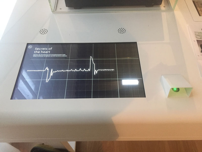 heartbeat sensor with visualisation
I also played with the PIR sensor during the machine building week. So I know in broad terms how you can connect a sensor and listen to its output.
what I want to learn
I do not have a specific learning goal for this week. I want to keep it simple, as the last two weeks (the motordriver that I never got to work and the group assignment) have taken a bit of a toll.
the process
group assignment
Probe an input device’s analog and digital signals.
I must admit, I spent a great part of the group assignment’s time debugging my motor driver board. So I missed the group assignment, but I did connect a thermistor to an Arduino board and tested its output. I was a bit puzzled at first, as the thermistor only had two wires, and I am used to sensors with 3 wires (VCC, GND and a signal wire). But this page showed me how it works. Basically, a thermistor is a resistor, and what you measure is the voltage on the line. The resistance is affected by the temperature, and therefor the voltage is as well. So it only needs two wires, one for ground and the other for vcc.
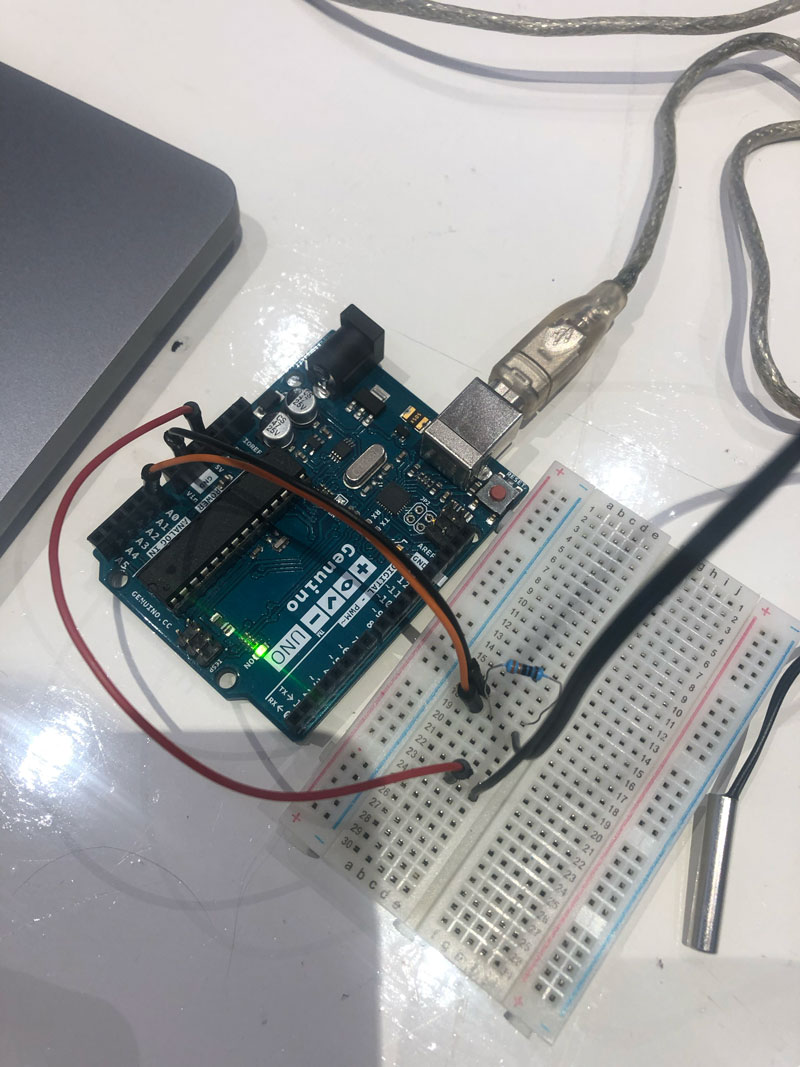 Arduino hooked up to the thermistor, with an extra resistor explained below
I used a NTC thermistor: a thermistor (or temperature sensor) that has a Negative Temperature Coefficient. This means that its resistance decreases as its temperature increases
So to have an idea about the temperature, we need to know the resistance of the thermistor. We have to calculate this, as the only value we are able to measure with the microcontroller of the Arduino is the voltage.
To calculate resistance from voltage, we add another resistor with a fixed value. Say for example 10K. During the regional review, I was informed that this is a common practice, which is called a Voltage Divider. In the lecture later that day, Neil mentioned he uses a Voltage Bridge rather than a divider, because it uses the whole range of the ADC instead of just the voltage between the two resistors. You can see this in his PCB design here. I will read up on both of these methods.
To calculate the resistance of the thermistor, we can use this formula where Vcc is the voltage from the Arduino (5V) and Vo is the voltage measured by the microcontroller:
Vo = R / (R + 10K) * Vcc
The unknown in this formula is R, the resistor value of the thermistor.
But Vo is known, this is the voltage that is measured.
We read the measured voltage with the AnalogRead method:
AnalogRead(pin_that_the_thermistor_is_connected_to);
This method gives a value between 0 and 1023. This value is not the voltage itself, but a digital number that reflects the voltage. The Analog to Digital Converter (ADC) is responsible for coming up with this number. It is calculated based on the assumption that 5V is the highest value: 1023 and 0V is the lowest value: 0. Any value in between is a ratio between those values, and is calculated with this formula:
Max ADC Value / Max Voltage = ADC reading / Analog Voltage Measured
Example
Let’s fill in the formula, assuming that the ADC reading has a value of 512
1023 / 5V = 512 / Analog Voltage Measured
We do some shuffling:
1023 * Analog Voltage Measured = 5V * 512
Analog Voltage Measured = (5V * 512) / 1023
Analog Voltage Measured = 2.50
(which makes sense, as 512 is half of 1023)
If we change the first formula to use the ADC conversion we get
(Vcc*ADC value) / 1023 = R / (R + 10K) * Vcc
or
ADC value / 1023 = R / (R + 10K)
or
ADC value = R / (R + 10K) * 1023
or
R = 10K / (1023/ADC) - 1
And now we are finally able to calculate the resistance of the thermistor, based on the AnalogRead input from the thermistor: For example, with an ADC value of 512 the resistance of the thermistor is:
R = 10000 / (1023/512) - 1
R = 10019.569
Ofcourse, we are not only interested in the resistance of the thermistor, but the temperature that you can derive from that. I looked it up, there is a formula far that too, but I did not go into it further as time was up and I needed to work on my individual assignment.
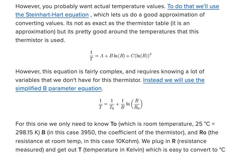 source:https://learn.adafruit.com/thermistor/using-a-thermistor
sidestep: Quentins Dual Serial
After a few weeks of programming with UPDI and testing with FTDI, I got a bit tired of fiddling with the boards all the time. Connect with UPDI for programming. Take out the little converter, turn the board around and stick it in the FTDI connector for serial monitoring. Test. Get it out, put the converter back, program again.
I knew that Quentin Bolsee designed a board with two connectors to do UPDI programming and serial monitoring at the same time and decided to spent some time milling and stuffing this board. This went without problems. After that, I needed to flash it with a binary that was linked from Quentins page. I used edbg for this. I had to tweak edbg, because I am on a mac. You can see how I did that here
Below is the terminal output for the edbg process. I listed the usb ports prior to flashing, and after it, and by the looks of the extra Atmel Corporation SAMD11, it might have gone right.
bvb:target bente$ lsusb
Bus 001 Device 001: ID 0a05:7220 0a05 Hub
Bus 001 Device 002: ID 6666:6666 6666 Generic CMSIS-DAP Adapter  Serial: B9B5F3D9
Bus 000 Device 000: ID 0a05:7220 0a05 USB 3.1 Bus
Bus 000 Device 001: ID 1d6b:0003 Linux Foundation 3.0 root hub

bvb:target bente$ ./edbg -ebpv -t samd11 -f dual_cdc_d11.bin
Debugger: Alex Taradov Generic CMSIS-DAP Adapter B9B5F3D9 v0.1 (S)
Clock frequency: 16.0 MHz
Target: SAM D11C14A (Rev B)
Erasing... done.
Programming..... done.
Verification..... done.

bvb:target bente$ lsusb
Bus 001 Device 001: ID 0a05:7220 0a05 Hub
Bus 001 Device 002: ID 6666:6666 6666 Generic CMSIS-DAP Adapter  Serial: B9B5F3D9
Bus 001 Device 003: ID 03eb:2425 Atmel Corporation SAMD11
Bus 000 Device 000: ID 0a05:7220 0a05 USB 3.1 Bus
Bus 000 Device 001: ID 1d6b:0003 Linux Foundation 3.0 root hub
When I tested in Arduino, I indeed got two usbmodem1110X ports. But when I tested with a loopback wire (connecting rx to tx on both connectors) only one of them gave me a proper echo in the serial monitor.
Later in the week I resoldered all the pins of the microcontroller. That fixed it: both ports now responded when I tested with a loopback.
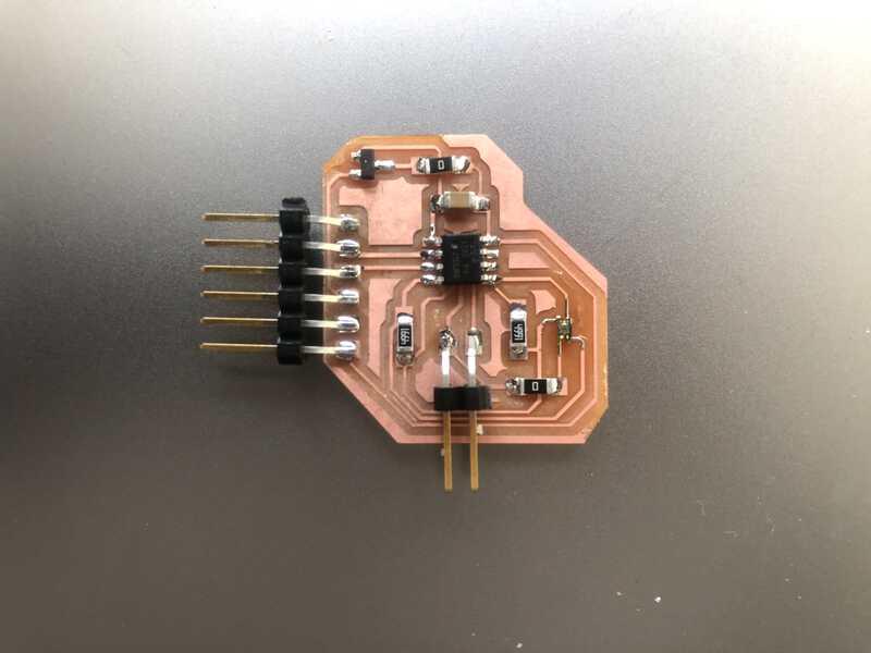
this weeks assignment: color sensor
Because my final project does not require an input device I am aware of, Henk suggested I tried out a color sensor. This sounded good to me, so I made a photo of the color sensor in the Waag Fab inventory to help me find the footprint in KiCad. I am looking for VEML6040:
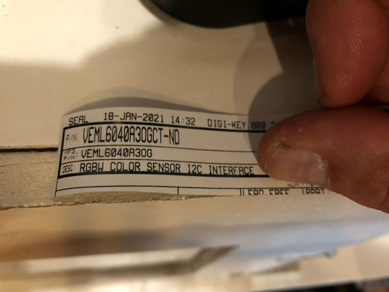
First I check Neils example, so I have something to guide me designing my own PCB. I find it here, and it reassuringly has the same name as the sensor Henk showed me.
However, in KiCad, this sensor is nowhere to be found. I do find a VEML6070, but that is a different sensor wih a different footprint. As I am sure the sensor is in the inventory, I decide to see if I can download and add the schematic and footprint for this sensor to my KiCad installation.
I find and download the footprint here and import it in KiCad with the following steps:
- In KiCad, go to Tools > Edit Schematic Symbols.
- Click on Preferences > Manage Symbol Libraries.
- In the Global Libraries tab, click on Add existing library to table, the small folder icon and navigate to the downloaded .lib file. Then click Open.
- Use the search bar on the left pane of the window to search for the imported symbol and double-click it to open.
The symbol that results from this action has the same 4 connectors as the example from Neil (VDD, GND, SCL, SDA) so I proceed to use it in my schematic.
On Neils example, I see the usual 1uF capacitor next to the microcontroller (Attiny412). Also 2 4.99k resistors and a 3.3V voltage regulator. This regulator is used because the color sensors operating voltage lies between 2.5V and 3.6V. There is also a 0K resistor, that I skip because I want to try to make traces without the need for a bridge. The voltage regulator is a little problem, because I have 3 versions to choose from in the Fab Inventory: 100mA, 150mA and 1A. The last one seems to be a bit too much for what I will put on this board. I select the 100mA one, as that is also the one that I used on Quentins Dual Serial board and it seems reasonable that the 5V USB input needs to be stepped down to 3.3V and that there is not so much current involved in a board with a AtTiny and a color sensor.
I also add an FTDI connector and 2 pin UPDI connector. I do not need 5V on the UPDI as I plan to use Quentins Dual Serial board that will provide 5V via the FTDI connector. When I look at Neils example after that I see he also has two pins for UPDI and and FTDI connector.
To make it still a bit of an exercise, I try to make the connections without looking at the example. Most of the things are easy to figure out. Except for the sensor, that is a bit too new. I check the datasheet and see a mention of a 0.1uF capacitor and pull-up resistors in a range of from 2.2 kΩ to 4.7 kΩ . Neil uses the two 4.99K resistors here, and this is because it is the value that comes closest (and is still higher) that is available in the Fab inventory.
In Kicad I see that the AtTiny has a pin for SCL (PA2) and SDA (PA1). As has the color sensor. As I do not know what SCL and SDA stand for, I decide to read up on I2C, the protocol that is used by this sensor.
I2C
This is a serial inter integrated circuit protocol. Which means that you can use it for communication between different IC’s. An AtTiny is an IC, as is a (color) sensor. It is a controller-responder or master-secondary protocol.
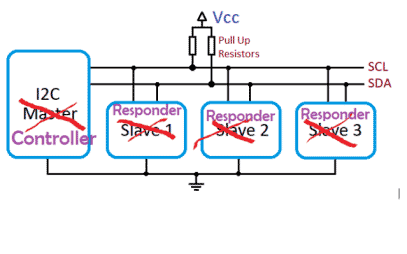
In my case, the AtTiny is the master, the sensor is the secondary. You can have multiple consecondaries per master, as you can have multiple masters per secondary.
With I2C, data is transferred in messages. It is an addressable protocol, which means that the master selects by address to which secondary to talk to. Every secondary has therefor its own address. All secondaries get the message, but only the secondary with the address that the master has sent will respond (with an ACK bit).
SDA stands for Serial Data, and this is the line for both master and secondary to send and receive data.
SCL stands for Serial Clock, the line that carries the clock signal. This is controlled by the master. The clock signal is used to synchronise the communication.
It seems reasonable to connect the SDA and SCL pins on both controllers to each other. But not without the pull-up resistors that connect the SDA and ACL pins to VCC.
PCB design
When I switch to the PCB designer in KiCad and import the schematics, I get an error message about a missing footprint of the VEML6040. I realise I only imported the schematic, and also need to import the footprint. I use the steps that are listed here under “Import Footprints” (a little below “Import Symbols”)
After that I reimport the schematic, and start working on the rats nest.
When I want to connect one of the pads of the sensor, I get an error: “The routing start point violates DRC”. I am guessing that DRC means Design Rules Constraints, and after some trial and error I find out that the 0.4mm track width in the Net Classes section of Board Setup is too much for this tiny sensor. It needs 0.25mm at the most. I check my documentation for a few weeks back, and see that the track width determined with the test pattern is 0.13mm with a one flute bit. So 0.25mm seems possible. I proceed, and change the track width to 0.25mm to draw the traces.
It is much harder than I expected. Somehow the pins of the colorsensor are positioned so that when connected to the proper pins on the AtTiny, they always form a closed circuit without possible outside connections. I try several ways, and in the end revert to the 0Ω resistor to make a bridge. I run into problems with the regulator as well. In Neils example, the GND line runs under his regulator. But the footprints that I use do not allow this. After some fiddling I give up and use a 0Ω bridge there as well.
When I run the DRC, I get an error about the clearance on the sensor. It should be 0.4mm (the width of the bit we use), bit it is 0.35mm. That means that the bit can not cut the trace there, and that the pads will stay connected. I know from a previous board that this is not too much of a problem, since I can always cut it with a knife.
Milling
Milling goes fine. As expected, the tiny pads of the sensor are connected to each other and together with Henk I try to cut them. This is a little bit harder than expected. One of the pads comes a bit loose from the board. That will be interesting when soldering.
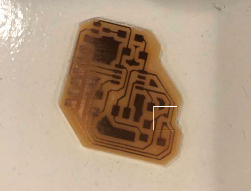 milled pcb, in the white rectangle the 2 pads that should be 4 pads
Stuffing
Henk advised to tin the pads, place the sensor and use the heatgun to do the actual soldering. So that is what I procceed to do.
That is harder than expected (again). The heatgun blows away the tiny sensor. So I try with the soldering iron. That works better for me. Eventually I have the sensor sticking to the board. But when I check the connections with a magnifier, I see that the cuts that I have made between the tiny pads have filled with solder. So I use the heatgun to get the sensor off the board and use the knife again to cut the pads loose. Then I reflow the solder, so each pad has clearly its own drop of solder and proceed to solder the sensor again, with the soldering iron. Barely daring to breath I get the sensor in place and by the looks of it this time without any shorts.
I select all the other components from the inventory. Compared to the sensor the resistors and capacitator are suddenly huge. Soldering them is a breeze. And then it is time for testing.
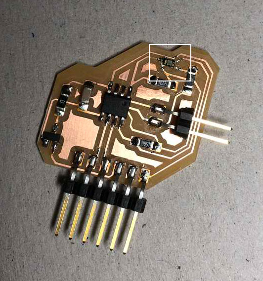 stuffed pcb, in the white rectangle the sensor
Testing
I connect my new board to the Dual Serial Board, so I can program and test it without having to switch connectors inbetween. I immediately notice that the regulator gets really hot. And when I try to upload a program I get the dreaded “UPDI initialisation failed”, meaning something somewhere is wrong.
I try with my old tried and tested FDTI board with UPDI connector, to rule out problems with the Dual Serial Board. But alas. I check the PCB design, take a good look at my board and realise I have the microcontroller upside down. So I take the heatgun, get the controller of and solder it back again in the correct position.
But again, I get the “UPDI initialisation failed”. I do a visual check of the traces and soldering, but everything looks fine. Even the sensor, although I do not fully trust my work there. I take a multimeter and test for shorts. I find a lot of them. Somehow somewhere something is not connected properly, but where?
The most obvious part is the sensor. Maybe I cut the traces not completely? Maybe the trace that came loose is bent and forms a short? I take it off, and solder it on again. Still shorts on the board. I check the GND trace that runs, a little bit too close, next to it. I cut away some excess solder that might make contact with it, but still problems. I take of the microcontroller again to inspect the traces that run under it, and do the same with the capacitor. Still shorts. I take of the sensor again, and the board has shorts even then. By then, the lab closes, and I go, a little bit frustrated, home.
I decide to abandon this board, as the traces around the sensor have become too bad after all the soldering and resoldering. At home, I redesign the board a bit. I create more space between the sensor and the surrounding traces. And I edit the (downloaded) footprint: I move the pads 0.05mm away from each other so there is exactly 0.4mm between them (instead of 0.35mm). This will make it possible to mill between these pads, so I do not have the cut them with a knife. I check the dimensions of the sensor first, and by the looks of it this 0.05mm will not cause problems.
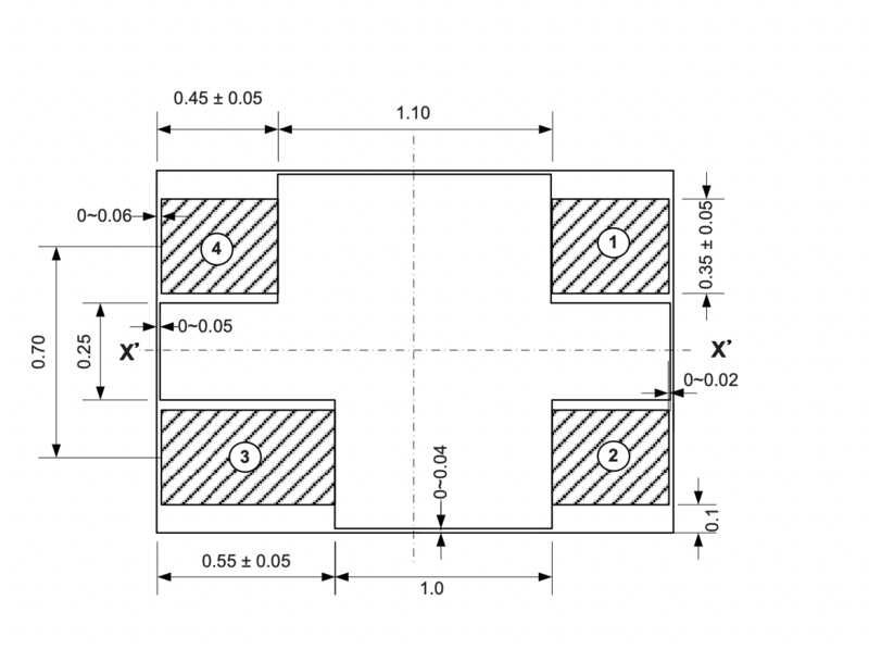 dimensions of the VEML6040 color sensor
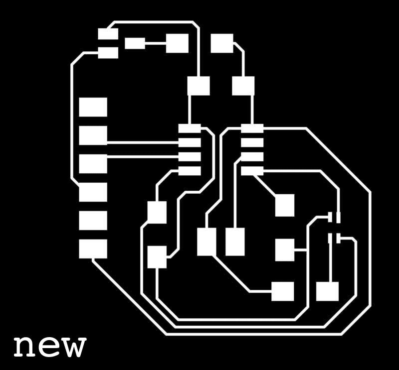 old traces compared to the new ones. More room around the sensor and between its pads
The new board
The next day I started with a freshly milled board. Unfortunatelty I forgot to take a picture before stuffing, but the tiny pads of the color sensor were nicely cut apart by a 0.4mm clearance. I took a little bit of flux, added some solder on the tip of the iron and touched the four pads so that they all had a little bit of solder. Then I placed the sensor on the pads (minding the correct orientation). I heat up one of the pads with the iron, solder flows, the sensor is fixated. I proceed to heat the other 3 pads, doublecheck with a magnifyer, reflow again, and finish of with the hotgun for good measure.
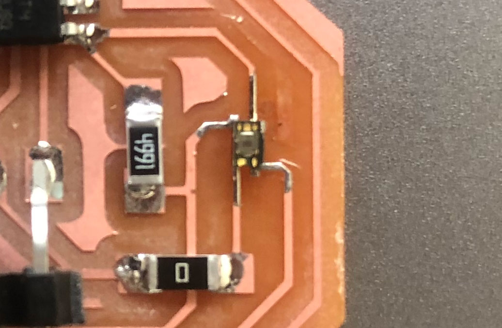 the new board with the sensor, will it work?
After soldering the remainder of the components, I take the multimeter and check for shorts. I find one, and realise I switched the capacitor and a 0Ω bridge. Phew! That I can fix. I desolder and resolder them in the correct positions and check again. No shorts this time. Then I take one of my programmer boards and upoad Neils example. Yes! Programming works! But does the sensor work? I take Quentins Dual Serial board, connect my board and check the serial output. Output!
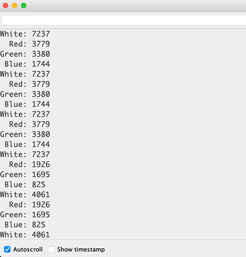 output from the sensor, note the different values for blue and red
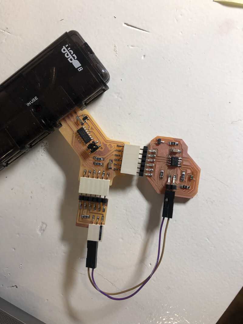 test setup with the Dual Serial board
looking back
what went wrong, what went well
It was a tough week again. Although I aimed to keep it simple with just one sensor on a board, there were a lot of things that were harder than expected:
-
the layout of the sensor and the layout of the microcontroller did not work nicely with each other.
I maybe tried too long to avoid the zero bridge -
the placemement and layout of the regulator also asked for a zero bridge
I also tried to avoid this for too long -
the clearance between the pads of the sensor was too small initially
I tried to fix that by cutting the pads after milling, but editing the footprint is a cleaner fix -
the sensor is so tiny
Soldering it was much harder than I thought. Having clean and sharp pads and using the flux + soldertip method worked best -
I got shorts on my board
The shorts came from the bad cut and solderjob on the sensor. Checking for shorts before testing the board seems like a good practice -
I built on a wonky base
I lost a lot of time with soldering the sensor on the pads that I tried to cut, and lost a lot of time by trying to fix the resulting shorts. On the new board with the better pads there was no problem at all and soldering was much easier