If you are into electronics, Printed Circuit Boards (PCBs) are the most common things you will see. These boards make our projects easier by eliminating all those connecting wires and breadboards. If properly designed, it will reduce the size of your device.
Learning:
- Group Assignment
-
Testing
-
GND (Ground) Continuity
-
VCC (5V) Continuity
-
VCC to GND Voltage
-
Testing
- Individual Assignment
- Design Echo Hello Board
- Soldering
- Programming
Group Assignments
Testing
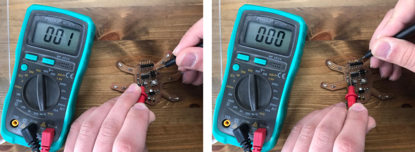
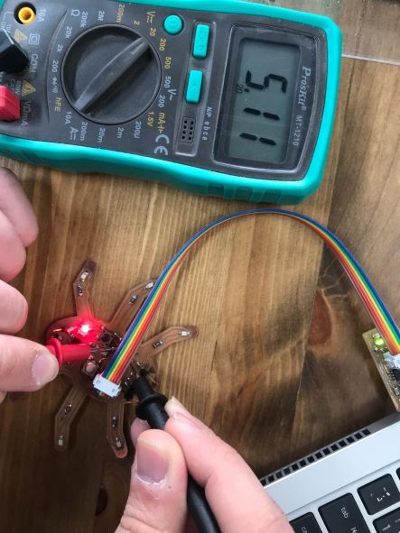
In group assignment we used the digital multimeter to check the continuity between ground pins and VCC pins. Also, we measured the VCC to GND voltage, which should be 5V.
GND (Ground) Continuity
We measured the continuity between the GND pins of the ATtiny44, SPI header and FTDI header. The digital multimeter should beep and read around 0 Ohm. This means all the three pins are connected.
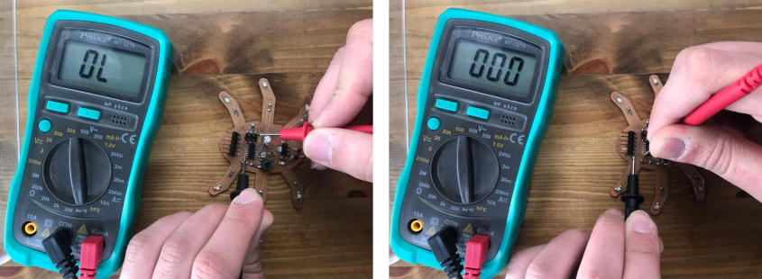
VCC (5V) Continuity
We measured the continuity between the VCC pins of the ATtiny44, SPI header and FTDI header. The digital multimeter should beep and read around 0 Ohm. This means all the three pins are connected.
VCC to GND Voltage
We connected the board to the FabTiny programmer and then to USB. We measured the voltage between the VCC pin and GND pin. The digital multimeter read 5V, which is the USB port voltage.
Individual Assignments
Design Echo Hello Board

In this week, I’ll talk about the process of designing a PCB. For me I chose EAGLE from Autodesk to design my board.
PCB design in EAGLE is a two-step process. First you design your schematic, then you lay out a PCB based on that schematic. EAGLE's board and schematic editors work hand-in-hand. A well-designed schematic is critical to the overall PCB design process. It will help you catch errors before the board is fabricated, and it'll help you debug a board when something doesn't work.
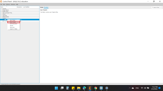
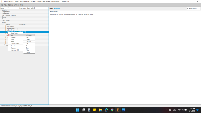
I started by making a new project folder for my design. In the control panel, under the Projects tree, right click on the directory where I want the project to be (by default EAGLE creates an "eagle" directory in the home folder), and select New Project.
The project folder will house both schematic and board design files. To begin the design process, I need to lay out a schematic. To add a schematic to a project folder, right-click the folder, hover over New and select Schematic.
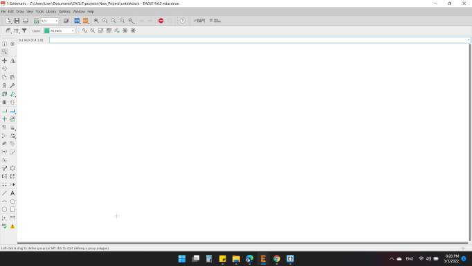
Immediately a new page open.
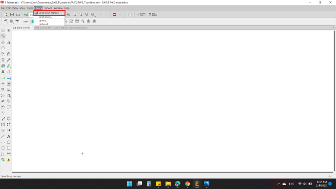
Before, when I was working at Fab Lab Irbid, I was using a library that contains most of the electronic parts, but I wanted to download and add the library they provided us with Fablabs Library.
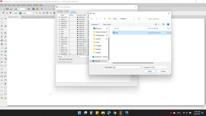
So, from Library then Open library manager.
Then in Available select Browse and open all components in the library.
The ADD tool -- ![]() -- is what you'll use to place every single component on the schematic. Here I used the library fab & fabirbid.
-- is what you'll use to place every single component on the schematic. Here I used the library fab & fabirbid.
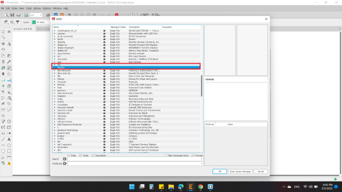
To actually add a component from a library either select the component you want and click "OK", or double-click your component.
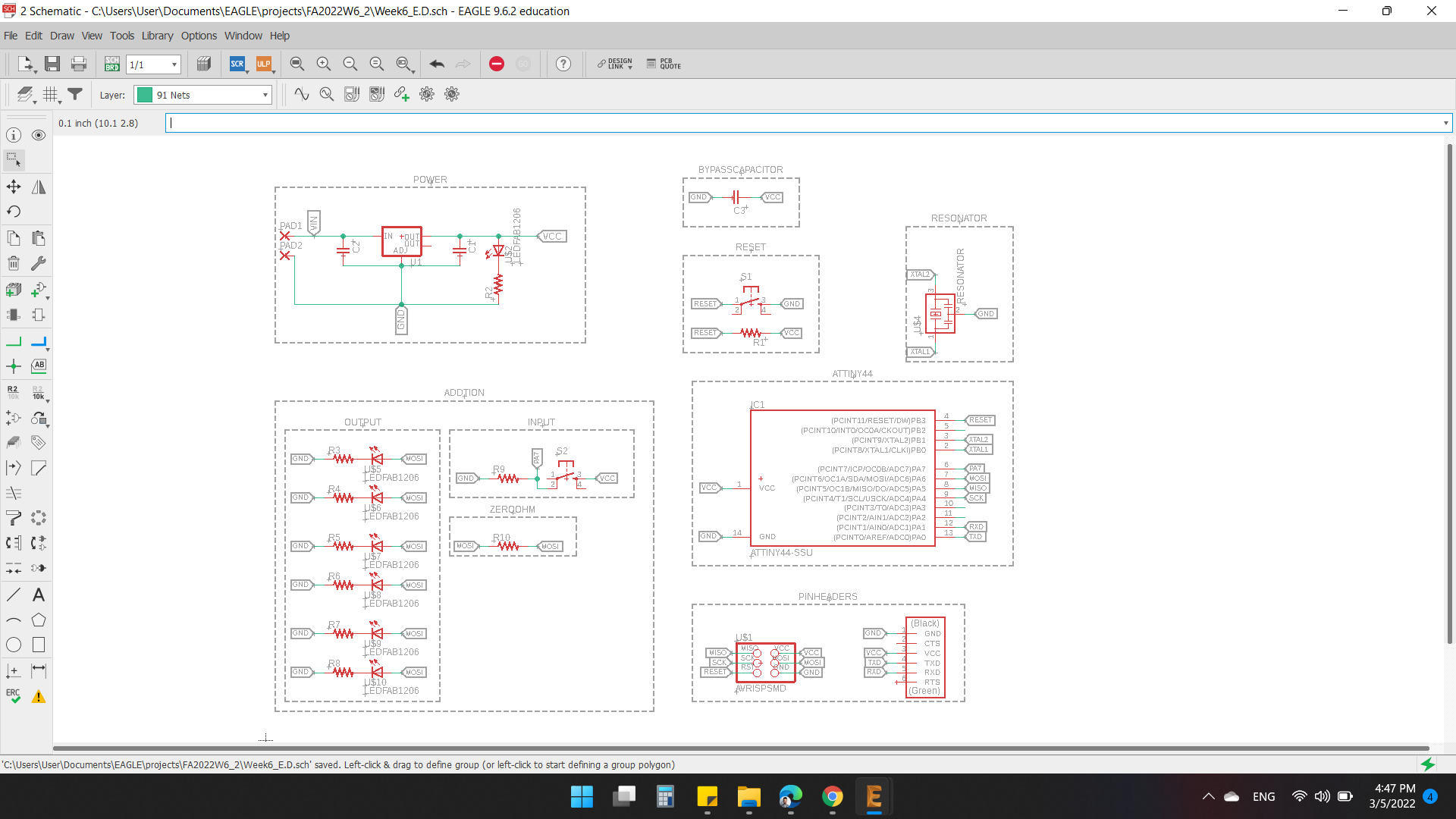
Schematics
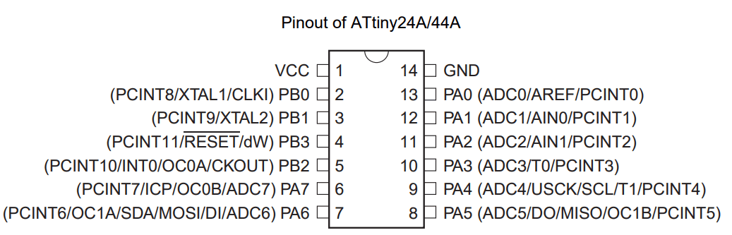
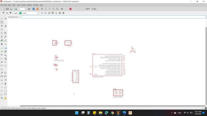
After I added fab & fabirbid libraries, I started to add the components. The first component is ATtiny44 which is an integrated circuit.
To understand where I'll connecting the other components, I took a look at the ATtiny44 Datasheet. The pinout is shown below.
Besides the first component, I added the rest of the components I needed.
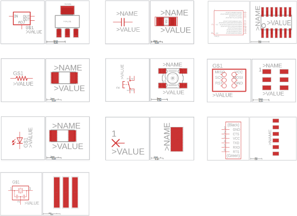
- ATtiny44 "ATTINY44-SSU SOIC14"
- Voltage Regulator"V_REG_LM1117SOT223"
- Capacitors"CAP-UNPOLARIZEDFAB"
- Resistors"RES-US1206FAB"
- Push Buttons"6MM_SWITCH"
- ISP AVR Male Header 2x3 SMD"AVRISPSMD"
- FTDI Male Header 6x1"FTDI-SMD-HEADER"
- LEDs"LEDFAB1206"
- Pads"SMD2_PAD"
- RESONATOR"Resonator"
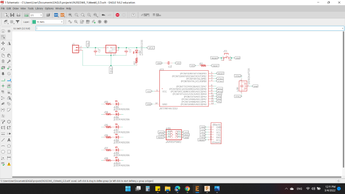
The NET tool -- ![]() -- it's a wire between the components.
-- it's a wire between the components.
The NAME tool -- ![]() -- that I used to avoid having wires all over the place.
-- that I used to avoid having wires all over the place.
I did a little trick; I named the main parts only, and left the other parts without names like leds and push button.
The reason is you have to connect the main parts first, you can't change the names of the parts because they are main, but the rest of the parts, just where to put them, find the nearest connect place and just tag it.
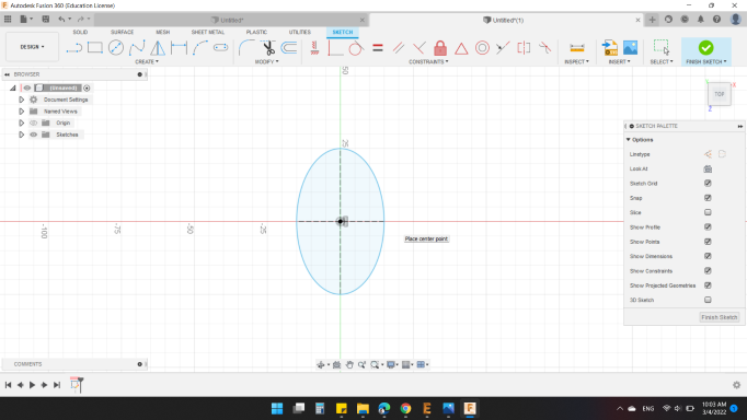
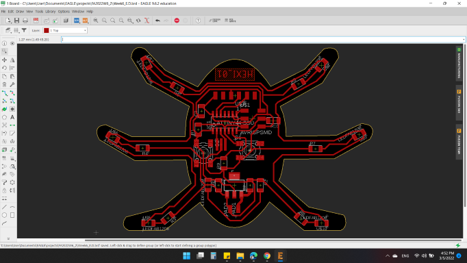
When I was choosing my electronic components, I thought of making a beautiful shape for the PCB.
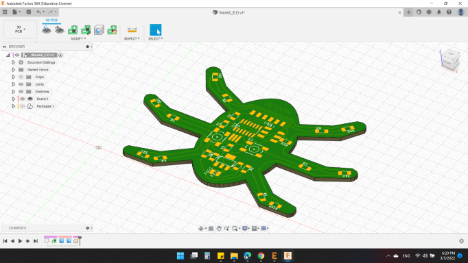
I went straight to my favorite software Fusion 360.
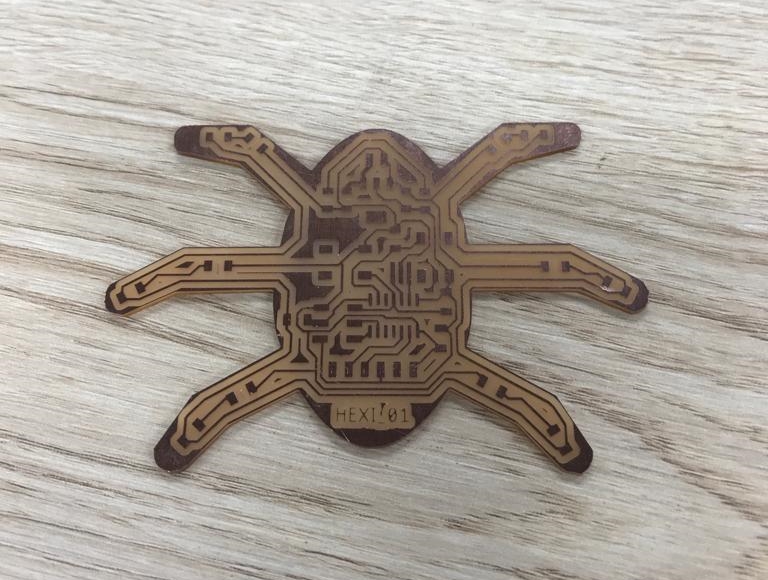
Since my final project is a hexapod robot, I thinked to make the shape looks like a spider. Using the ellipse shape, I sketched the main body.
And added an upper limb.
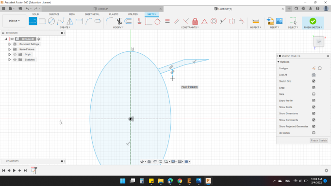
By Patterns and Mirror, I built the rest limbs.
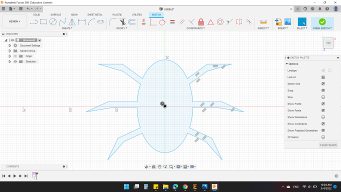
Finally, I added Fillets for the corners to reduce acute protrusion.
Board
To generate your board design, just press -- ![]() -- Generate/switch to board in the schematic window.
-- Generate/switch to board in the schematic window.
When you turn your schematic into a PCB layout file, you’ll get a new window that looks like this.
When you are in Board desgin window, presss on -- ![]() -- to Switch to Schematic window.
-- to Switch to Schematic window.
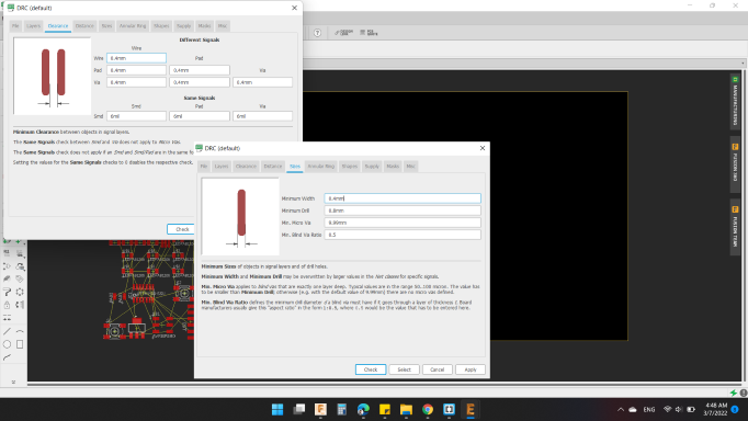
Before start routing, you need to check the Design Rule Check "DRC" -- ![]() -- where I select Clearance and Sizes as the picture below.
-- where I select Clearance and Sizes as the picture below.
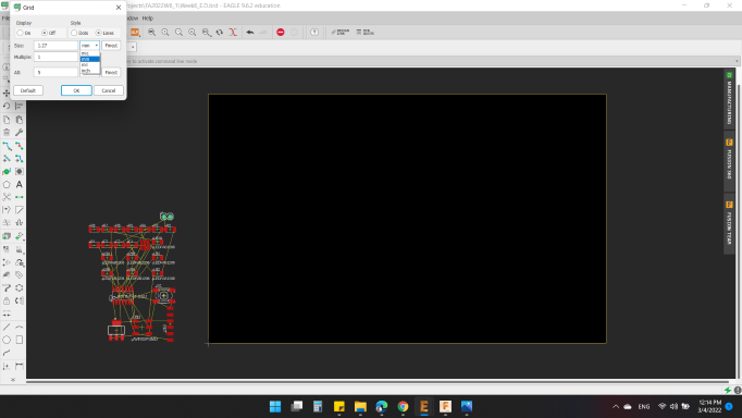
Then, I modified the Grid unit -- ![]() -- to mm.
-- to mm.
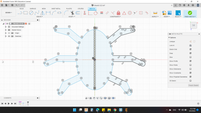
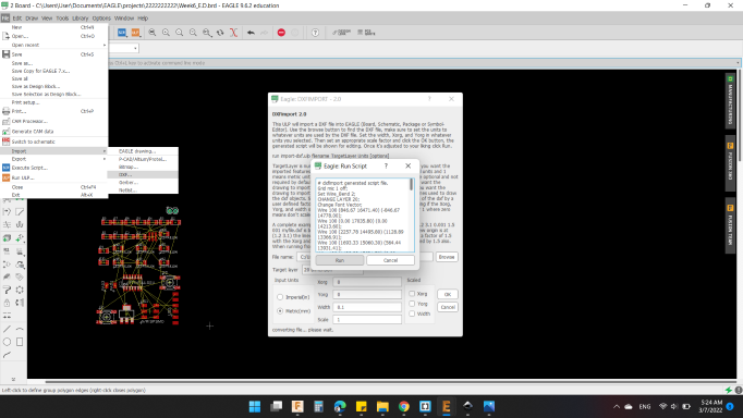
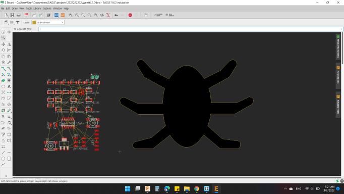
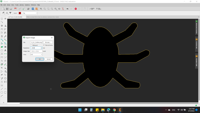
Finally for the setup, I imported the sketch dxf from Fusion 360 to be the outline of the PCB, and deleted the yellow rectangle.
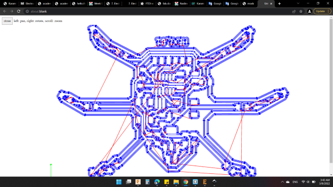
And here's the outline shape.
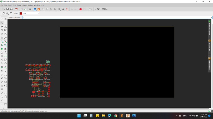
Before I start distributing the components, I changed the CONN_01 into SMD2_PAD.
And brought the electronic parts that are already connected from the FAB ACADEMY site to connect the components as the picture.
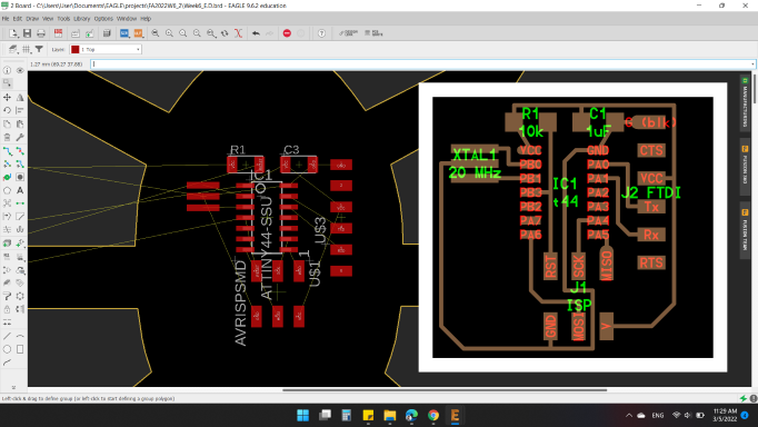
After that, I started Routing by press Route Airwire -- ![]() -- To be able to do routing, you can change the position and orientation of the components to find the easiest way to route them.
-- To be able to do routing, you can change the position and orientation of the components to find the easiest way to route them.
You’ll also notice a bunch of lines connecting between your components. These are called airwires. You might also hear it referred to as a Ratsnest -- ![]() --. What ratsnest does is that it shortens the connections between the components for easy routing.
--. What ratsnest does is that it shortens the connections between the components for easy routing.
As I mentioned at the beginning, I'll connect the major parts first, and then, according to the distribution of the rest of the minor parts, I'll name them.
After I distributed the rest of the parts (LED's and Resistors), I found the closer pin and can be connect to them is MOSI. And for Push Button to pin PA7.
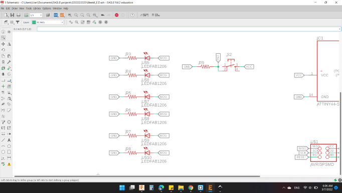
Actually I needed a zero ohm resistor, I hit a dead end, so I had to use it.
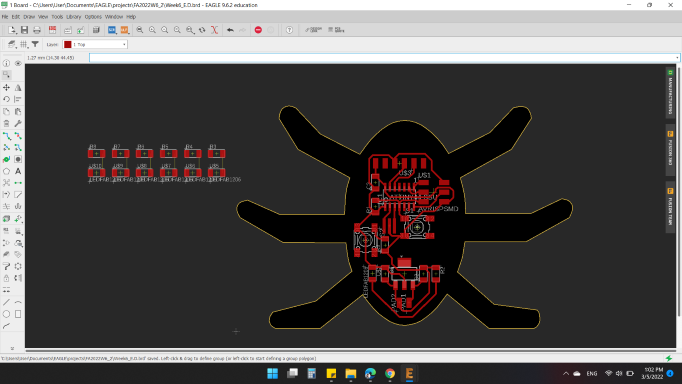
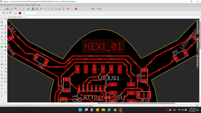
I decided to name the pcb relative to my final project. So HEXI_01 is the name!
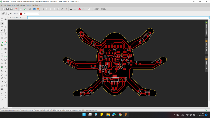
And here the board ready by connections.
And finalized the schematic by collect the components into groups.
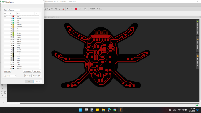
To save the the design, We must hide all layers from Layer Settings -- ![]() -- and keep Top Layer.
-- and keep Top Layer.
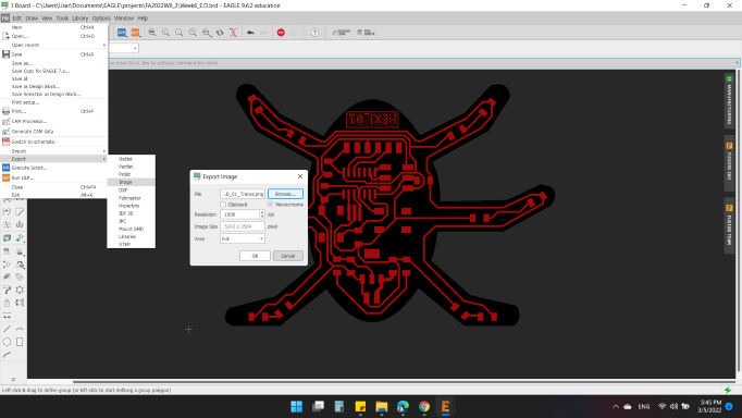
Then export the file as image.
- File: Week6_E.D_01_Traces
- Monochrome: "YES"
- Resolution" 1500 dpi
Next, I hid all layers one more time, then showed the Dimension Layer. And export file as image again.
- File: Week6_E.D_01_Outline
- Monochrome: "YES"
- Resolution" 1500 dpi
The images are almost done, one more thing to do.
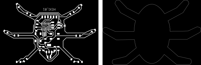
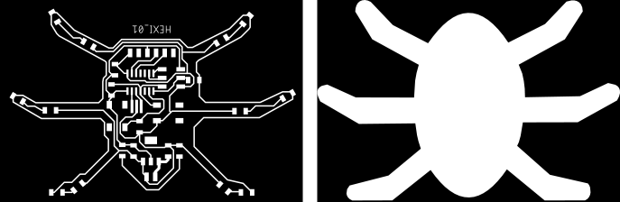
For the Outline image, the cut occurs between black and white, and because Outline image has black on the outside and the white line and black on the inside, the cut will happen twice (between the black outside with white, and between the black inside with white), so one difference must be kept (black outside with white).
What I did is I brought the image into the Paint, and I filled the inner black space with white, and here is the result.
Mods
After that I inserted the images to the Fab Mods set the settings for the Traces as seen below.
- Mill Traces (1/64)
- Tool Diameter
- mm: 0.39624 / in: 0.0156
- Cut Depth
- mm: 0.1016 / in: 0.004
-
Max Depth
- mm: 0.1016 / in: 0.004
-
Offset Number
- 4
-
Speed
- 4 mm/s
-
Origin
- x = 0 mm, y = 0 mm, z = 0 mm.
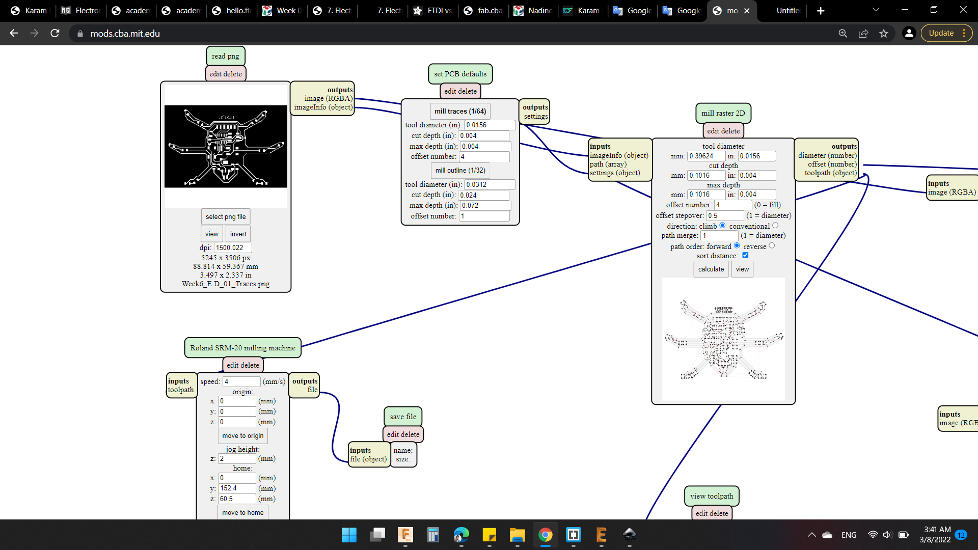
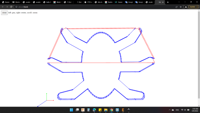
And the tool path:
For the Outline.
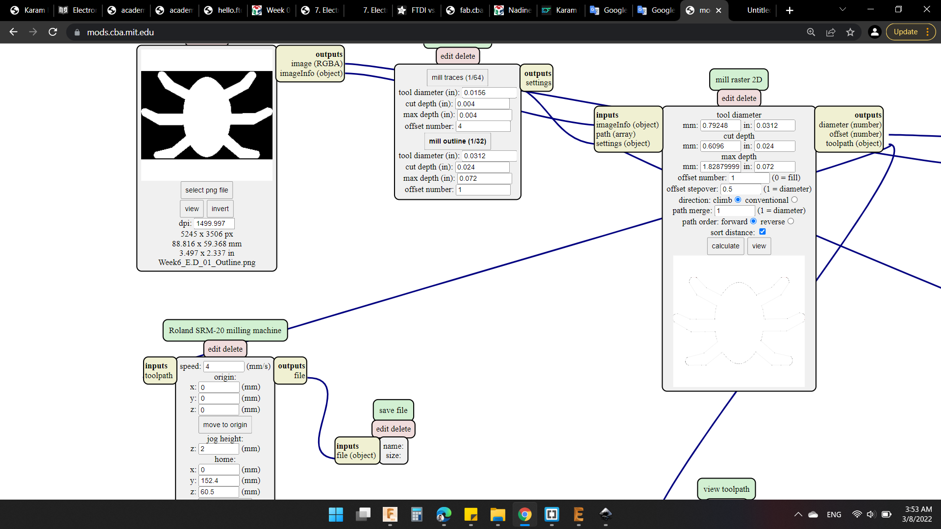
- Mill Outline (1/32)
- Tool Diameter
- mm: 0.79248 / in: 0.0312
- Cut Depth
- mm: 0.6096 / in: 0.024
-
Max Depth
- mm: 1.8287999999999998 / in: 0.072
-
Offset Number
- 1
-
Speed
- 4 mm/s
-
Origin
- x = 0 mm, y = 0 mm, z = 0 mm.
Then I calibrated the Roland SRM-20, chose the X & Y and the zero for the Z.
Here's the Traces cut and Outline cut.
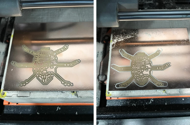
And here's my HEXI_01 PCB : ).
I wanted to see the board in 3D model. So by clicking in Fusion 360 icon at the right, a new window shown.
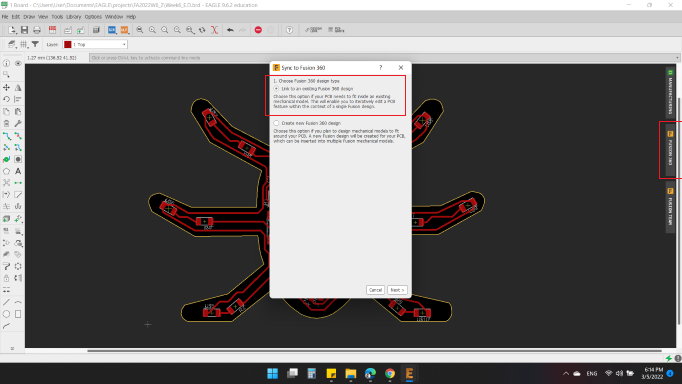
then selet the folder to create the 3D model.
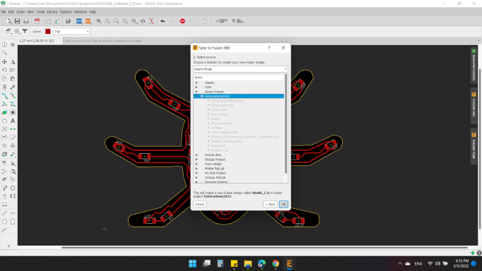
Automatically the file pushed to Fusion 360.
And here's the model in Fuison 360.
Soldering
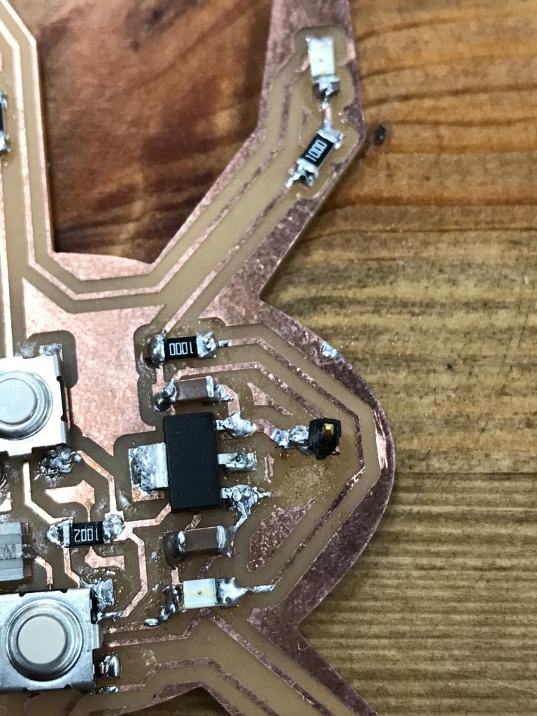
Now it's time to solder the components.
My PCB needs the following components:
- ATtiny 44 >> 1
- Voltage Regulator 5v >> 1
- Resonator 2o MHz >> 1
- Capacitor unpolarized 1uF >> 3 (2 with V.R and 1 close to the IC)
- Push Button >> 2
- Resistor 100 Ohm >> 7 (6 at the corrner and 1 for the V.R)
- Resistor 10 KOhm >> 1 (Pullup resistor with push button)
- Resistor 0 Ohm >> 1
- LED >> 7
- ISP Header 3x2 >> 1
- FTSI Header 6x1 >> 1
- Header 2x1 >> 1 (with V.R)
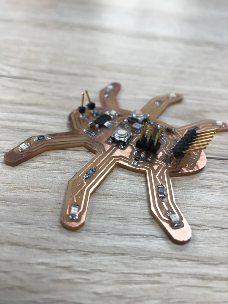
And these components stick to the board : ).
Unfortunately, while soldering the penultimate piece, I cut the trace that connected to the ground. Luckily I was able to connect the trace and it worked again.
Finally, my HEXI_01 pcb is alive : ).
Programming
The third part of electronics is to program the board that I designed using Arduino. I had a simple background on how to deal with Arduino, So I did not find much difficulty in dealing with programming.
To work my PCB, I should program it, and to program it I should using the Arduino as a programmer, so I used the Arduino as an ISP to programe my board.
The Arduino ISP is an In-System-Programmer that is used to program AVR microcontrollers.
First, I searched in google about attiny arduino github, then click on installation guide to follow these steps in this tutorial.
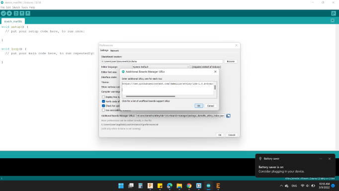
Then, I copied the below URL link to used in Arduino Software (IDE).
https://raw.githubusercontent.com/damellis/attiny/ide-1.6.x-boards-manager/package_damellis_attiny_index.json
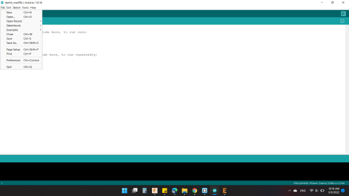
Next, I opened ![]() Arduino IDE Software.
Arduino IDE Software.
Then, "Preferences" in Arduino.
The dialog shows the preferences, in the "Additional Board Manager URLs" I clicked to paste the link that I have copied.
Next, I wanted to define the Attiny44 into Arduino, I opened "Boards Manager".
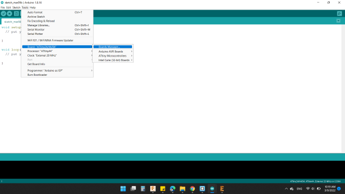
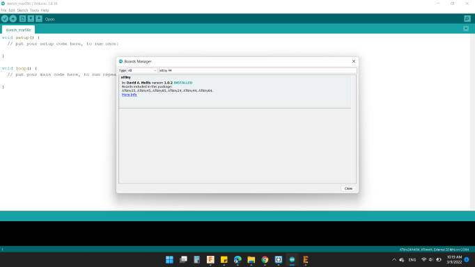
Then I wrote in the search Attiny44 to install it. I define the ATtiny boards in the Arduino environment, because the Arduino boards it was not built in ATtiny boards.
After that, I did a Google search on Arduino UNO as ISP Pinout for an image, to know which pins that are [VCC, GND, REST, MOSI, MISO and SCK]
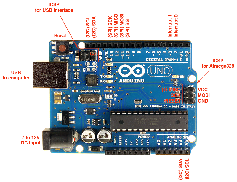
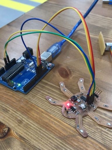
Then, I connected Arduino to the laptop by USB data sync cable for Arduino, and the PCB board to Arduino by jumper wires according to the image above.
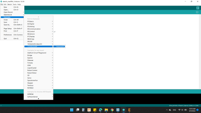
Next, I programmed the Arduino as ArduinoISP using the examples available in the Arduino IDE by following the below steps.
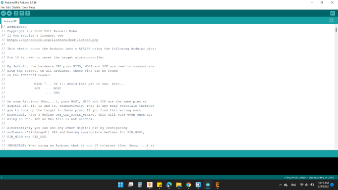
The new dialog shows the code that make the Arduino as programmer.
Then I clicked on "tools" and choose the options below.
- Board: Arduino/Genuino Uno
- Port: COM3
- Programmer: Arduino as ISP
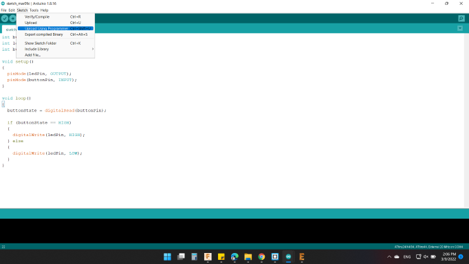
This code upload on Arduino to be a programmer by click on ![]() .
.
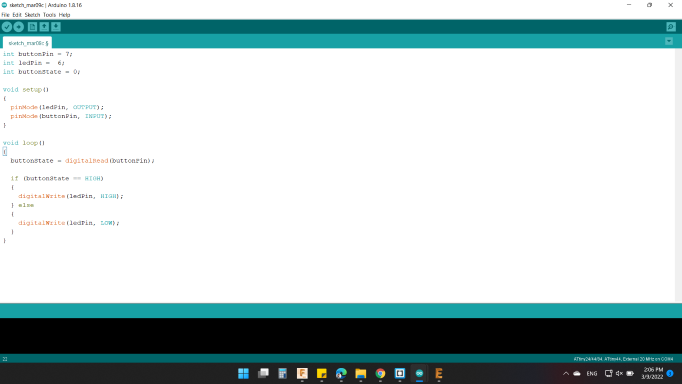
I wanted to write a code that lights both LED, but one after another and the time between them is half a second. The image below shows the code.
Then I clicked on "tools" and choose the options below.
- Board: ATtiny25/45/85
- Processor: ATtiny44
- Clock: Internal 8 MHz
- Port: COM3
- Programmer: Arduino as ISP
After that, I clicked on "Burn Bootloader" from the "tools", the ISP programmer will start to burn the bootloader into the target Arduino. It usually takes few seconds to complete burning bootloader. Arduino IDE will display "Done burning bootloader" when it is done. You can read about Bootloader.
Finally, I clicked on "Upload Using Programmer" to upload the code to the PCB board.
For more effects, I turned the lights off and run HEXI_01 : ).
***Note:
This week I noticed that 4 LED's only work when I connect the board through the ISP Pin Headers and the remaining two don't. And when I connect the board through the Voltage Regulator, the remaining two only work and the four do not work.
After thinking and going back several times for the scheme and consulting some friends, I discovered a simple mistake I had made and it is not my fault 😜
Go to the Week8 "Embedded Programming", where I explained what happened in detail.
You can download my files here: