6. Embedded Programming
Reflection
In 2022, I really struggled at googling every term inside the datasheet and there were many gaps which i cant find online. In 2024, it was more doable to read the datasheet with Chatgpt but I couldnt remember everything hence I tried to read the datasheet and then use chatgpt to answer my doubts. Before are records of the information, i read from internet search and chatgpt. it was paraphrased by me so may have some errors, if you spot any do let me know. The theory are drop down, do click to see the reading i did. For other assignments i also did this type of search for all the definitions which fabacademy taught but i did not understand. Its in my document but commented out or some are removed but can be seen only if you checkout the old branches before i remove theory sections. I agree with my instructor that currerntly my skills still lacking so better to remove it first. Only left the theory in this assignment as this assignment was the only one where i was instructed to document what i read. My colleagues noticed that whenever i had free time at work during 2023, i will be googling the terms, youtubing extra information, udemying to learn from people claiming to be experts, chatgpting the bigger ideas. which was so arcane to me.
Group Assignment
Attached is the link to group assignment
Individual Assignment
Checklist for this week:
- ☑ Linked to the group assignment page --Done
- ☑ Documented what you learned from browsing through a microcontroller datasheet -- Done as much as I can not for ATTINY1614, sure how in depth must i go.
-- Did Datasheet for ATTINY1614 as initially, my final project was using a light box using ATTIny1614 and bluetooth. As instructor mentioned that it may not be sufficient to pass, I was changed final project to slope and ESP32C, but I really do not want to delete the attiny1614 read and reread a full datasheet reading for esp32c3.
-- Under I2, I described the key differences of attiny1614 and esp32c3 in the data sheet.
- ☑ Programmed your board to interact and communicate -- Fully made a board using EasyEda and did not made a programmer, used arduino as programmer which was not acceptable for Fabacademy. Did ESP32C3 programming and read basics of the datasheet.
- ☑ Described the programming process(es) you used -- Code in Adruino
- ☑ Included your source code -- Done here Blink Code for ATTINY1614 Pins Test for ATTINY1614Comms Test for ATTINY1614
- ☑ Included 'hero shot(s)' -- Included Pictures.
I1. Programme ATTINY1614 with Arduino
I programmed the ATtiny1614, I start with setting up my Arduino IDE to support ATtiny devices, followed by transforming my Arduino Uno into a UPDI programmer using the jtag2updi firmware. This method allows for programming the ATtiny1614 with custom code, such as a simple LED blink program. The connection setup involves linking the Arduino Uno and ATtiny1614 through their respective power and UPDI communication pins. With the Arduino IDE properly configured for the ATtiny1614 and the jtag2updi programmer, I uploaded the blink sketch to the ATtiny1614. The table below outlines these actions and provides reasoning for each:
| Action | Details | Reason |
|---|---|---|
| Install Arduino IDE | I ensured the Arduino IDE is installed from the official Arduino website. | Provides the necessary environment to write, compile, and upload sketches. |
Add MegaTinyCore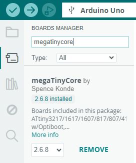
|
I Added the MegaTinyCore board manager URL to the Arduino IDE and install it. | Enables support for ATtiny series microcontrollers, including ATtiny1614, within the Arduino IDE. |
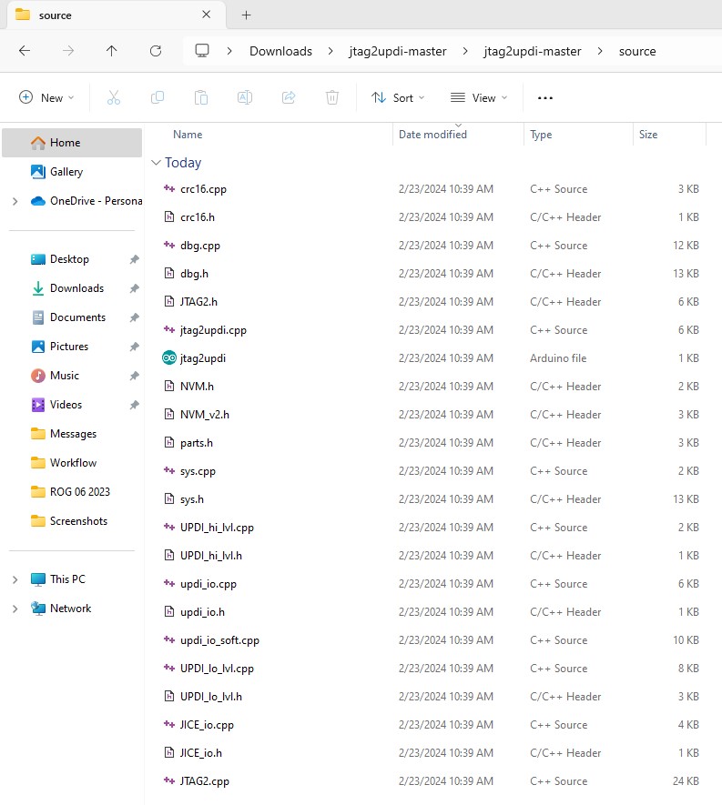
Download jtag2updi Firmware
|
I Obtained the jtag2updi firmware from GitHub and prepare it for upload. | Allows the Arduino Uno to function as a UPDI programmer, essential for programming ATtiny devices. |
Upload jtag2updi to Arduino 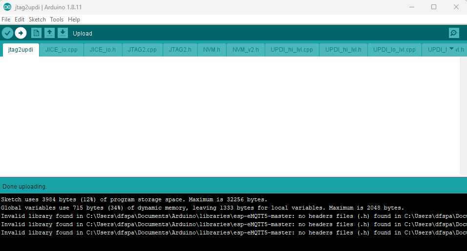
|
I Uploaded the jtag2updi sketch to the Arduino Uno, converting it into a UPDI programmer. | Transforms the Arduino Uno into a tool capable of programming the ATtiny1614 via UPDI. |
| Hardware Setup | I connected the Arduino Uno to the ATtiny1614 as per UPDI programming requirements. Just one wire from Arduino to UPDI and one common ground. | Establishes the physical connection necessary for the UPDI programming process. |
Select Board and Programmer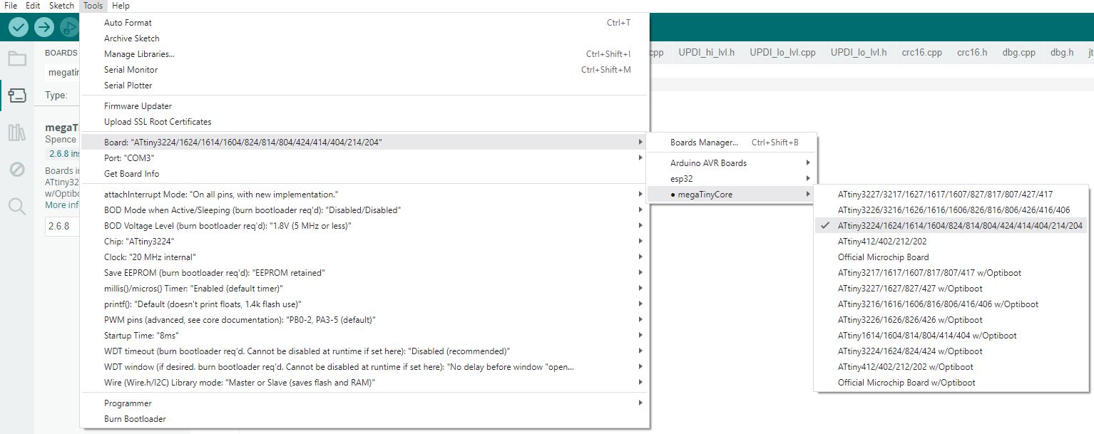 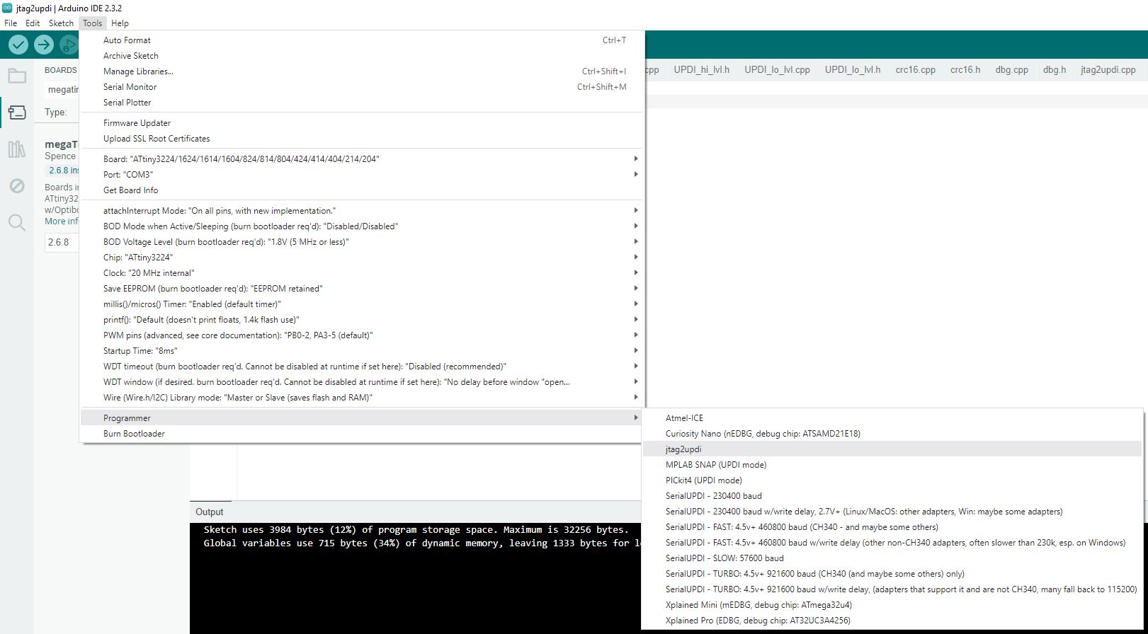 |
In the Arduino IDE, I select the ATtiny1614 board and jtag2updi as the programmer. | Configures the IDE to communicate with the ATtiny1614 using the correct programming protocol. |
Write Blink Sketch
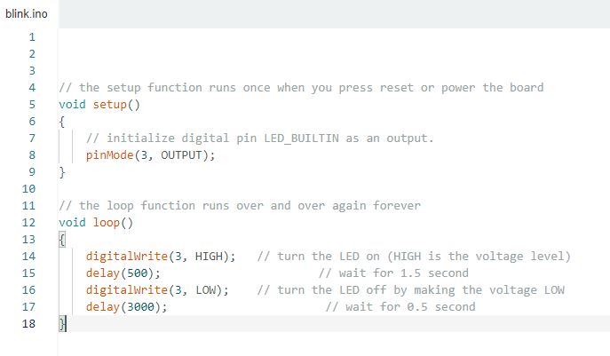 |
I Create a blink sketch in the Arduino IDE tailored for the ATtiny1614. Pin 3 is being used | Demonstrates the capability of the ATtiny1614 by executing a simple LED blink program. |
Upload Sketch 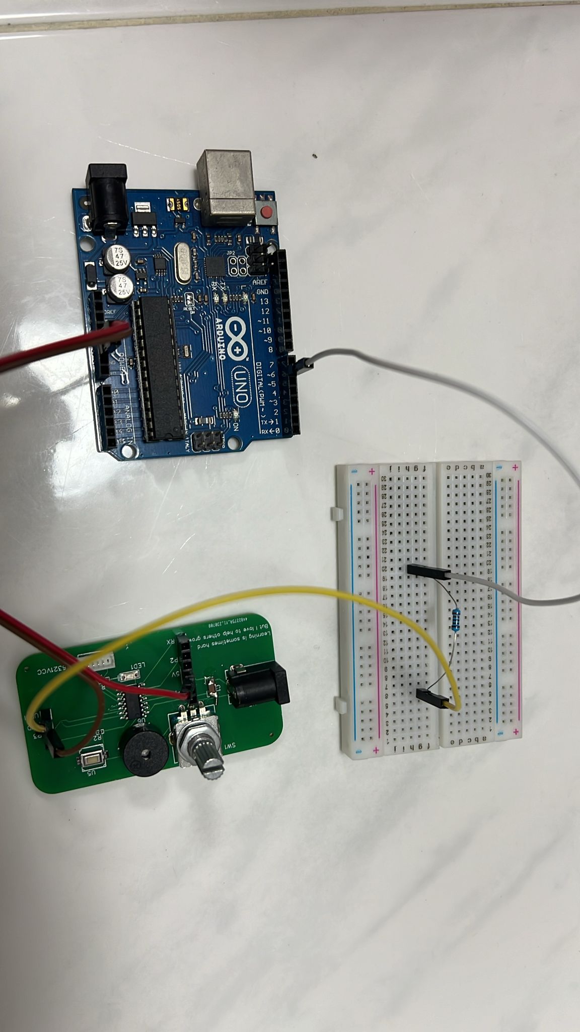 |
I Use the Arduino IDE to upload the blink sketch to the ATtiny1614 via the UPDI connection. | Transfers the user-created program to the ATtiny1614, enabling it to perform the blink operation. |
I understand from my instructor that I have to redo as I need to code ATTINY1614 with my own programmer instead of arduino programmer. As I am using Xiao_ESP32C3, I will be writing how to programme ESP32 Xiao
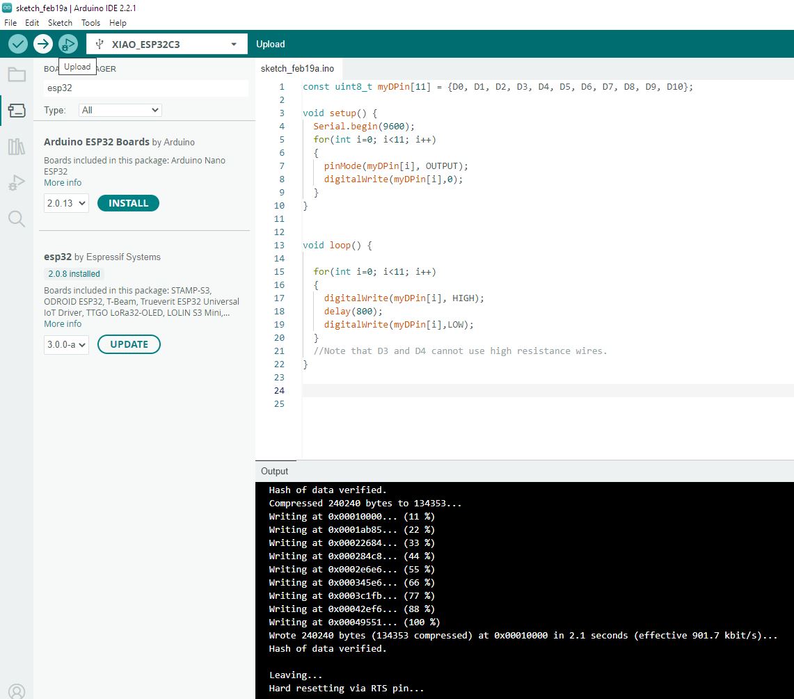
I2. Individual Assignment- ESP32-C3 Xiao Programming
This section outlines the steps necessary to program the ESP32-C3 Xiao module using the Arduino IDE.
| Action | Details |
|---|---|
| Install Arduino IDE | I downloaded and installed the latest version of the Arduino IDE from the official Arduino website. |
Add ESP32 Board Support
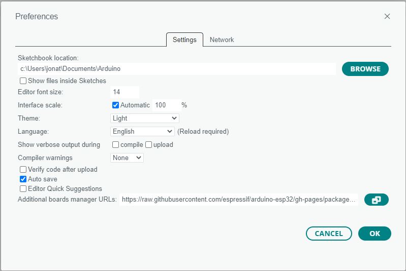 |
I opened the Arduino IDE, navigated to File > Preferences, and add the ESP32 boards manager URL to the Additional Board Manager URLs field. The URL can be found on the official Espressif GitHub or Seeed Studio documentation for the ESP32-C3. |
Install ESP32 Board Package
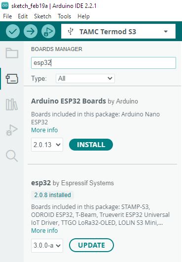 |
Went to Tools > Board > Boards Manager, searched for "ESP32", and installed the latest version of the ESP32 by Espressif Systems. |
Select Your Board
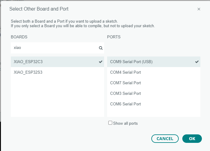 |
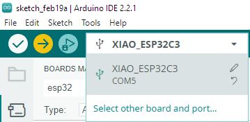
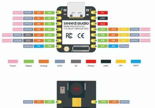
Under Tools > Board, navigated to the ESP32 Arduino section and selected the Seeed Studio Xiao ESP32-C3 board. Mine was Xiao_ESP32C3, Note: choosing the wrong module will cause error during pin assignment. |
Choose COM Port
 |
I connected my ESP32-C3 Xiao to my computer via USB. Then selected the correct COM port under Tools > Port. |
Prepare Code
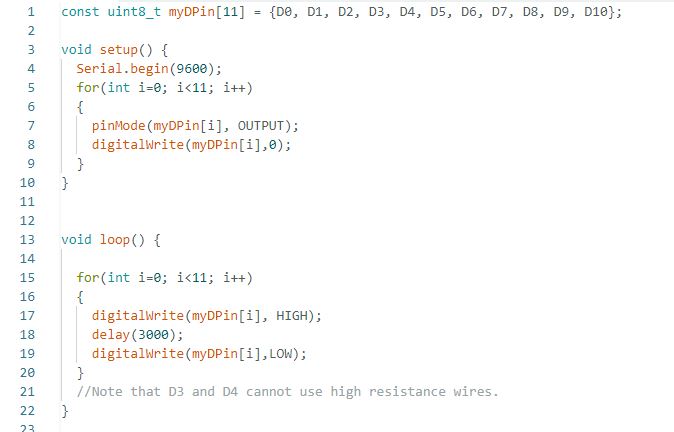 |
I Wrote my code in the Arduino IDE. The code which I wrote allows me to check all the pins of the Microcontroller. I also wrote code so that the ESP32 can detect button preess and light up LED. Lastly, I wrote code so that the ESP32 can communicate with my pc, Where i send a string on my serial monitor and it displays the string sent. |
Compile and Upload
|
I clicked the "Upload" button in the Arduino IDE to compile code and upload it to the ESP32-C3 Xiao. I ensured that no errors are present in the compilation and uploading process. |
| Verify All pins working
|
Once the code is uploaded, I monitored the ESP32-C3 Xiao's output for all the 11 pins. |
| Tested Local Input and Output
|
Coded ESP32 to take detect button pressed and turn on led |
| Tested Communication | Coded ESp32 to take words type into serial comms and esp32 response by outputing the words typed. |
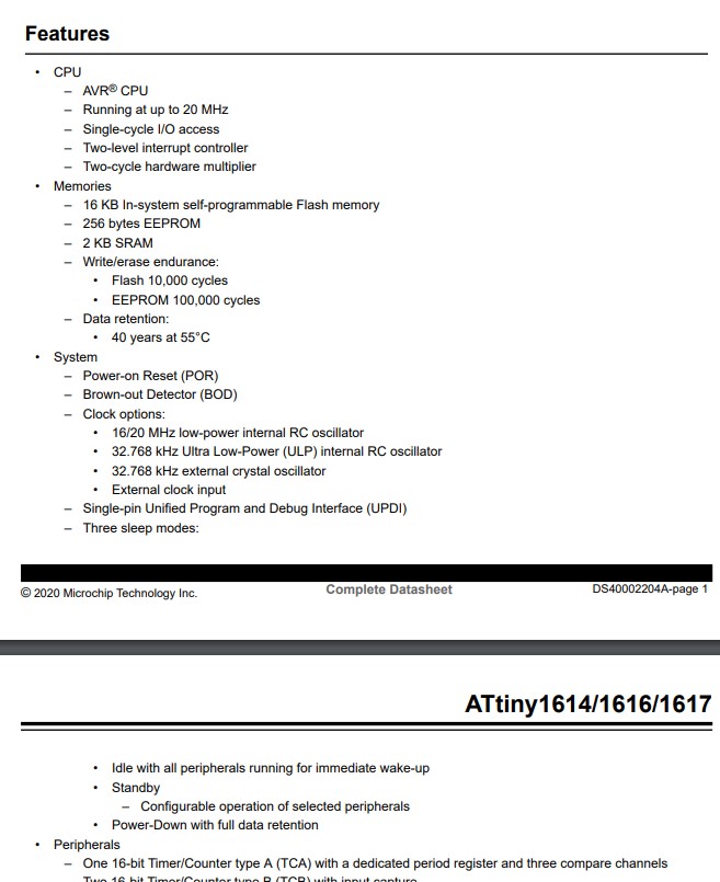
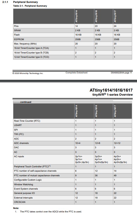
I3. Important Information in Datasheet for ATTINY 1614
Below is the collection of basic important points about microcontrollers for my reference in future. I will surely forget.
| Data Point | Why It's Important | Other Important Information |
|---|---|---|
| Microcontroller Core | Identifies the processing core, which determines the instruction set, architecture, and efficiency. The ATTINY 1614 uses an AVR core, known for its simplicity and power efficiency. | Knowing the core is essential for selecting the appropriate compiler and development tools. |
| Operating Voltage | The voltage range in which the microcontroller can operate safely. For the ATTINY 1614, this is typically between 1.8V and 5.5V, allowing flexibility in battery-powered and low-power applications. | Choosing components that match the operating voltage is crucial for system stability and longevity. |
| Memory Specifications | Details the size of Flash, SRAM, and EEPROM. The ATTINY 1614 offers 16KB of Flash, 2KB of SRAM, and 256B of EEPROM, affecting program size and variable storage capacity. | Memory size impacts the complexity and functionality of the software that can be run. |
| I/O Pin Count and Configuration | Specifies the number and types of input/output pins. The ATTINY 1614 has 14 GPIO pins, which determine how many external devices or sensors can be interfaced. | Understanding pin functions (e.g., PWM, ADC capabilities) is key for designing the hardware interface. |
| Clock Speed | Indicates the maximum operating frequency, with the ATTINY 1614 supporting up to 20 MHz. This affects how quickly the microcontroller can execute instructions. | Higher clock speeds can increase performance but also power consumption. |
| Communication Interfaces | Lists supported communication protocols (e.g., I2C, SPI, UART). This is vital for determining how the microcontroller can communicate with other devices. | Selection of communication interfaces affects compatibility with peripherals and other microcontrollers. |
| Power Consumption | Provides information on power usage under various conditions, important for battery-powered and energy-efficient designs. | Designing for low power consumption is crucial in portable and IoT devices to extend battery life. |
| Package Types | Describes the physical packaging of the IC, which affects how it can be mounted on a PCB. The ATTINY 1614 is available in multiple packages, including SOIC, QFN, and VQFN. | The choice of package can impact the manufacturing process and overall design footprint. |
I4. Reading Datasheet for ATTINY 1614 -- Summary Page
Below is the data on all the attiny1614 terms for page 1 on its CPU
| Feature | Description | ATTINY1614 vs Arduino |
|---|---|---|
| AVR® CPU | The microcontroller's central processing unit, based on the AVR architecture known for its simplicity and efficiency. | The ATTINY1614 and Arduino (like Uno which uses ATmega328P) both use AVR CPUs, but the ATTINY1614 may have fewer resources due to its smaller size. |
| Running at up to 20 MHz | The maximum operating frequency of the CPU. Higher MHz allows the CPU to process instructions faster. | The ATTINY1614 can potentially run faster than many Arduino boards like the Uno, which typically run at 16 MHz. |
| Single-cycle I/O access | Input/Output operations can be completed in one cycle of the CPU clock, enhancing performance. | Both the ATTINY1614 and many Arduino boards offer single-cycle I/O access for efficient peripheral management. |
| Two-level interrupt controller | A system that handles interrupts on two priority levels, allowing certain processes to be prioritized over others. | Arduinos also feature interrupt controllers, though the complexity and number of levels can vary based on the specific MCU used. |
| Two-cycle hardware multiplier | A hardware feature that allows multiplication operations to be completed in two cycles of the CPU clock, which is fast for a microcontroller. | Most Arduinos with AVR processors also include a hardware multiplier, though the number of cycles for the operation may vary. |
This section is for the pg1 for memories
| Feature | Description | ATTINY1614 vs Arduino Uno (ATmega328P) |
|---|---|---|
| Flash Memory | Stores the executable code that the microcontroller runs. | The ATTINY1614 has 16 KB of Flash, which encourages efficient coding practices due to its limited size. In contrast, the Arduino Uno comes with 32 KB of Flash memory. This difference highlights the ATTINY1614's suitability for smaller, dedicated applications, whereas the Arduino Uno can accommodate larger programs and is thus better suited for projects that may evolve in complexity. |
| EEPROM | Non-volatile memory for storing small amounts of data that must persist through power cycles. | With only 256 bytes of EEPROM, the ATTINY1614 is designed for storing essential configuration data or small amounts of information crucial to the device's operation. The Arduino Uno provides 1 KB of EEPROM, offering more space for data storage, which can be particularly useful for projects requiring the retention of more extensive user data or operational parameters across sessions. |
| SRAM | Short-term memory used by the microcontroller when it's powered on and running a program. | Both devices are equipped with 2 KB of SRAM. This equal amount suggests that, for temporary operational data storage, both microcontrollers are on an even playing field. The impact on performance from SRAM would therefore be similar, making either choice viable for projects where SRAM capacity is a critical factor. |
| Write/Erase Endurance | Reflects the lifespan of the memory in terms of write and erase cycles before failure. | The ATTINY1614 offers a Flash endurance of 10,000 cycles and EEPROM endurance of 100,000 cycles. This is generally in line with what the Arduino Uno offers, suggesting that both microcontrollers are designed to withstand a significant amount of programming and reprogramming activities. The higher EEPROM endurance of the ATTINY1614 may give it a slight edge in applications requiring frequent updates to stored data. |
| Data Retention | The duration that the EEPROM can retain data without power at a given temperature. | The ATTINY1614 promises data retention of 40 years at 55°C, indicating its reliability over long periods, which is critical for applications where the microcontroller may be deployed in field operations without regular maintenance. This specification matches the reliability expected from Arduino Uno's components, ensuring both are suitable for projects where long-term data retention is necessary. |
This section is for the pg2 for system
| Feature | Description | Significance in Prototyping |
|---|---|---|
| Dedicated Period Register and Three Compare Channels | Includes a dedicated register for setting the period of the timer and three compare channels for comparing the timer value against predefined values. | Provides versatile timer functionality for tasks such as generating precise PWM signals, measuring time intervals, and event scheduling. |
| Two 16-bit Timer/Counter type B (TCB) with Input Capture | Features two 16-bit timer/counters with input capture capability, allowing for capturing external events and measuring pulse widths. | Enables accurate time measurement, frequency counting, and pulse width modulation, essential for various timing-sensitive applications. |
| One 12-bit Timer/Counter type D (TCD) optimized for Control Applications | Optimized for control applications, providing a 12-bit timer/counter with enhanced features for precise timing and control tasks. | Facilitates efficient control algorithms, motor control, and synchronization tasks in embedded systems, enhancing system performance and responsiveness. |
| One 16-bit Real-Time Counter (RTC) | Operates from an external crystal, external clock, or internal RC oscillator, providing accurate real-time clock functionality. | Enables timekeeping, event scheduling, and accurate timestamping of events in applications requiring real-time operation, such as data logging, scheduling, and synchronization. |
| Watchdog Timer (WDT) with Window mode | Includes a watchdog timer with Window mode, along with a separate on-chip oscillator for timing. | Enhances system reliability by monitoring and resetting the microcontroller within a specified time window, preventing system hangs or malfunctions. This is particularly useful in critical applications where system stability and uptime are paramount, such as industrial control systems and safety-critical devices. |
| One USART with fractional baud rate generator | Features a USART with a fractional baud rate generator, auto-baud detection, and start-of-frame detection. | Facilitates serial communication with other devices, providing flexible baud rate options, automatic synchronization, and frame detection for reliable data transmission. This is essential for communication-intensive applications such as data logging, wireless communication, and sensor networks. |
| One master/slave Serial Peripheral Interface (SPI) | Includes a master/slave Serial Peripheral Interface for communication with other SPI devices. | Enables high-speed, full-duplex serial communication between microcontrollers, sensors, displays, and other peripherals, essential for data exchange and interfacing with external devices. This feature is commonly used in applications requiring fast data transfer rates, such as multimedia devices, real-time control systems, and networking equipment. |
| One Two-Wire Interface (TWI) with dual address match | Features a Two-Wire Interface (TWI) compatible with Philips I2C, supporting dual address matching. | Facilitates easy interfacing with I2C-compatible devices such as sensors, EEPROMs, and other peripherals, allowing for efficient data exchange and communication in embedded systems. The dual address match capability enhances flexibility in addressing multiple devices on the same bus, enabling more sophisticated communication protocols and device management. |
| Philips I2C compatible | Compatible with the Philips I2C protocol for communication with I2C-compatible devices. | Ensures compatibility and interoperability with a wide range of I2C devices, simplifying system integration and enabling seamless communication in embedded projects. This compatibility allows developers to leverage existing I2C peripherals and libraries, reducing development time and effort while ensuring reliable communication with external devices. |
| Fast mode (Fm, 400 kHz) | Supports I2C communication in fast mode, with a data rate of 400 kHz. | Enables faster data transfer between the microcontroller and I2C-compatible devices, allowing for quicker response times and improved system performance in applications requiring high-speed communication, such as sensor networks and real-time control systems. |
| Fast mode plus (Fm+, 1 MHz) | Enhanced version of I2C fast mode, supporting a higher data rate of 1 MHz. | Offers even faster data transfer capabilities compared to standard fast mode, enabling ultra-fast communication between the microcontroller and I2C devices. This is beneficial for applications demanding extremely high-speed data exchange, such as high-resolution imaging, audio processing, and video streaming. |
| Three Analog Comparators (AC) with low propagation delay | Includes three analog comparators with minimal propagation delay for fast response. | Facilitates rapid comparison of analog signals, enabling quick decision-making and control in applications requiring real-time signal monitoring, threshold detection, and analog signal processing. |
| Two 10-bit 115 ksps Analog-to-Digital Converters (ADCs) | Features two 10-bit ADCs with a sampling rate of 115 ksps (kilo samples per second). | Enables high-speed and accurate conversion of analog signals to digital data, essential for acquiring sensor data, measuring analog inputs, and implementing closed-loop control systems in real-time applications such as motor control, instrumentation, and data acquisition. |
| Three 8-bit Digital-to-Analog Converters (DACs) with one external channel | Includes three 8-bit DACs for converting digital data to analog signals, with one external channel for additional flexibility. | Provides analog output capabilities for generating precise voltage levels, controlling analog circuits, and interfacing with external devices such as displays, actuators, and audio devices. The presence of an external channel enhances versatility by allowing connection to external analog components or peripherals. |
| Voltage Reference 0.55V | Provides a voltage reference of 0.55 volts. | Offers a low-level reference voltage for precision analog circuits, sensor interfaces, and low-power applications where minimal power consumption and high accuracy are required. |
| Voltage Reference 1.1V | Provides a voltage reference of 1.1 volts. | Serves as a standard reference voltage for many analog-to-digital converters (ADCs) and digital-to-analog converters (DACs), ensuring consistent and accurate conversion of analog signals in embedded systems. |
| Voltage Reference 1.5V | Provides a voltage reference of 1.5 volts. | Commonly used as a reference voltage for sensor calibration, signal conditioning, and power management circuits in various electronic devices and systems. |
| Voltage Reference 2.5V | Provides a voltage reference of 2.5 volts. | Used as a stable reference voltage for voltage regulation, precision measurement, and sensor interfacing in embedded systems requiring higher accuracy and performance. |
| Voltage Reference 4.3V | Provides a voltage reference of 4.3 volts. | Serves as a higher-level reference voltage for applications requiring wider voltage ranges, such as audio amplification, power management, and motor control, providing adequate headroom and dynamic range for signal processing and control. |
| Event System (EVSYS) | Provides CPU-independent and predictable inter-peripheral signaling. | Facilitates efficient communication and coordination between peripherals without CPU intervention, enabling seamless interaction and synchronization between different modules and subsystems in complex embedded systems. This feature enhances system scalability, flexibility, and responsiveness, allowing for the implementation of advanced event-driven architectures and real-time control strategies. |
| Configurable Custom Logic (CCL) | Includes two programmable look-up tables for custom logic operations. | Enables users to implement custom digital logic functions directly within the microcontroller, eliminating the need for external logic gates or additional components. This feature enhances design flexibility, reduces system complexity, and improves performance by offloading logic operations from the CPU, making it ideal for implementing application-specific functions, protocol converters, and interface controllers. |
| Automated CRC Memory Scan | Automatically scans memory contents for CRC errors. | Enhances system reliability and data integrity by detecting and correcting errors in non-volatile memory without CPU intervention. This feature is particularly useful in safety-critical applications, data storage systems, and communication protocols where data integrity is paramount, ensuring robust and error-free operation even in harsh environments or during power fluctuations. |
| Capacitive Touch Buttons, Sliders, Wheels, and 2D Surfaces | Supports capacitive touch sensing for various user interface elements such as buttons, sliders, wheels, and 2D surfaces. | Enables the implementation of intuitive and responsive touch interfaces in embedded systems, enhancing user interaction and experience. This feature is ideal for applications requiring user input or control through touch-sensitive interfaces, such as consumer electronics, industrial control panels, and wearable devices. |
| Wake-up on Touch | Allows the microcontroller to wake up from low-power sleep modes upon detecting a touch event. | Enables power-efficient operation by allowing the system to remain in a low-power state until user interaction is detected. This feature is essential for battery-powered devices and energy-efficient designs, extending battery life and optimizing power consumption in portable and battery-operated applications. |
| Driven Shield for Improved Moisture and Noise Handling Performance | Utilizes a driven shield to improve moisture and noise handling performance in capacitive touch sensing applications. | Enhances signal integrity and reliability by minimizing the impact of environmental factors such as moisture and electromagnetic interference (EMI), ensuring accurate and stable touch detection even in challenging operating conditions. This feature is beneficial for outdoor devices, industrial equipment, and automotive applications exposed to harsh environments. |
| Up to 14 Self-Capacitance Channels | Supports up to 14 self-capacitance sensing channels for touch detection. | Provides flexibility in designing touch interfaces with multiple touch-sensitive areas or buttons, allowing for versatile user interaction and control options. This feature is suitable for applications requiring a moderate number of touch inputs, such as home appliances, consumer electronics, and control panels. |
| Up to 49 Mutual Capacitance Channels | Supports up to 49 mutual capacitance sensing channels for touch detection. | Offers expanded touch sensing capabilities for applications requiring a large number of touch inputs or complex touch interfaces, such as interactive displays, kiosks, and gaming consoles. This feature enables designers to create sophisticated touch-based user interfaces with enhanced functionality and responsiveness, catering to diverse user interaction requirements. |
| External Interrupt on All General-Purpose Pins | Allows external interrupts to be triggered on all general-purpose input/output (GPIO) pins. | Enhances flexibility and responsiveness in event-driven applications by enabling the microcontroller to respond to external events or signals on any pin, without restricting interrupt functionality to specific pins or dedicated interrupt lines. This feature is valuable for implementing real-time event handling, sensor interfaces, and interrupt-driven tasks in embedded systems, providing versatility and ease of integration for various peripheral devices and sensors. |
I5. Reading Datasheet for ATTINY 1614 -- Content Page
Below is the table to guide how to use the content page
| Question | Important Parameters | Data Sheet Section | Example Question and Answer |
|---|---|---|---|
What are the key configuration settings summarized in the Configuration Summary section, and how can they impact the behavior and functionality of the ATtiny1614 microcontroller in a prototype?
 |
Pin, SRAM, EEPROM, Max Frequency, Counter, Communication, Watchdog | Configuration Summary | Question: What are the key configuration settings summarized in the Configuration Summary section, and how can they impact the behavior and functionality of the ATtiny1614 microcontroller in a prototype? Answer: The Configuration Summary section provides a concise overview of important configuration settings such as clock sources, clock division factors, and system clock prescalers. Understanding these settings is crucial as they directly influence the overall performance, power consumption, and timing behavior of the microcontroller in a prototype. By configuring these settings appropriately based on the application requirements, you can optimize the performance and efficiency of the ATtiny1614 in your design. |
| How does the Block Diagram illustrate the internal architecture and functional blocks of the ATtiny1614, and how can it aid in understanding the connectivity and interaction between different components in a prototype? | Block Diagram | Block Diagram | Question: How does the Block Diagram illustrate the internal architecture and functional blocks of the ATtiny1614, and how can it aid in understanding the connectivity and interaction between different components in a prototype? Answer: The Block Diagram provides a visual representation of the internal architecture and functional blocks of the ATtiny1614 microcontroller, including the CPU core, peripherals, memory units, and I/O ports. By studying this diagram, you can gain insights into the connectivity and interaction between different components, understand the data flow and signal paths within the microcontroller, and identify key functional blocks relevant to your prototype. This understanding is essential for designing and debugging hardware and software components, as well as optimizing system performance and resource utilization in your design. |
| What are the available pin configurations? | Package Options: 14-Pin SOIC, 20-Pin SOIC, 20-Pin VQFN, 24-Pin VQFN | Pinout | Question: How many pins are available in the 14-Pin VQFN package? Answer: There are 14 pins available in the 14-Pin VQFN package. |
| What considerations should be made for I/O multiplexing? | Multiplexed Signals, Pin Functionality, Pull-up/Pull-down Options | I/O Multiplexing and Considerations | Question: What is the default pin functionality of GPIO pin PA0? Answer: The default pin functionality of GPIO pin PA0 is ADC input. |
| What types of memory are available? | Flash Program Memory, SRAM Data Memory, EEPROM Data Memory | Memories | Question: How much SRAM data memory is available in the ATtiny1614? Answer: The ATtiny1614 has 512 bytes of SRAM data memory. |
| What peripherals are integrated, and where are they mapped? | Peripheral Address Map | Peripherals and Architecture | Question: What is the address of the Timer/Counter0 control register? Answer: The Timer/Counter0 control register is mapped at address 0x00B0. |
| What is the CPU architecture, and what are its features? | Register Summary, Functional Description | AVR CPU | Question: What is the size of the General Purpose Registers (GPRs) in the ATtiny1614? Answer: The General Purpose Registers (GPRs) are 8 bits wide in the ATtiny1614. |
| How can nonvolatile memory be controlled? | Nonvolatile Memory Controller Features | NVMCTRL - Nonvolatile Memory Controller | Question: What are the features of the Nonvolatile Memory Controller (NVMCTRL) in the ATtiny1614? Answer: The NVMCTRL in the ATtiny1614 supports read, write, and erase operations on the Flash memory. |
| What are the key functionalities and capabilities provided by the Nonvolatile Memory Controller (NVMCTRL)? | Overview, Functional Description, Register Summary, Register Description | NVMCTRL | Question: Can you explain the role of the Nonvolatile Memory Controller (NVMCTRL) in the ATtiny1614 and its significance for prototyping? Answer: The NVMCTRL is a crucial component responsible for managing nonvolatile memory operations, including reading, writing, and erasing Flash memory. It plays a vital role in storing program code and data persistently, ensuring data integrity and reliability in the prototype. |
| How do the clocking options provided by the Clock Controller (CLKCTRL) impact prototyping decisions? | Available Clock Sources, Clock Frequency | CLKCTRL - Clock Controller | Question: Why is it essential to carefully select the clock source and frequency when prototyping with the ATtiny1614? Answer: The clock source and frequency significantly influence the performance, power consumption, and timing requirements of the prototype. By understanding and appropriately configuring the clocking options provided by the CLKCTRL, prototypers can ensure optimal operation and efficiency of their designs. |
| How can the Sleep Controller (SLPCTRL) features be leveraged to optimize power management in the prototype? | Sleep Modes, Power Consumption | SLPCTRL - Sleep Controller | Question: In what ways can the Sleep Controller (SLPCTRL) contribute to power optimization in an ATtiny1614 prototype? Answer: The SLPCTRL offers various sleep modes that allow the microcontroller to enter low-power states during idle periods, reducing overall power consumption. By strategically utilizing these sleep modes based on the prototype's operational requirements, prototypers can achieve efficient power management and prolong battery life. |
| How does the Reset Controller (RSTCTRL) impact the initialization and startup process of my prototype? | Features, Overview, Functional Description, Register Summary, Register Description | RSTCTRL - Reset Controller | Question: What role does the Reset Controller (RSTCTRL) play in the initialization and startup sequence of the ATtiny1614, and how can understanding its features benefit my prototype? Answer: The RSTCTRL section provides insights into the various reset sources, reset options, and startup procedures available in the microcontroller. By exploring this section, you can understand how to configure the reset behavior of the ATtiny1614 to ensure proper initialization and reliable operation of your prototype under different conditions. |
| How can the CPU Interrupt Controller (CPUINT) facilitate task scheduling and event handling in my prototype? | Features, Overview, Functional Description, Register Summary, Register Description | CPUINT - CPU Interrupt Controller | Question: What functionalities does the CPU Interrupt Controller (CPUINT) offer, and how can they assist in managing task scheduling and event handling in an ATtiny1614 prototype? Answer: The CPUINT section provides mechanisms for managing and prioritizing interrupts generated by various sources in the microcontroller. By understanding and appropriately configuring these interrupt handling features, you can implement efficient task scheduling and event-driven behavior in your prototype, ensuring timely response to external events and optimal utilization of CPU resources. |
| How does the Event System (EVSYS) enhance inter-peripheral communication and coordination in my prototype? | Features, Overview, Functional Description, Register Summary, Register Description | EVSYS - Event System | Question: In what ways does the Event System (EVSYS) facilitate inter-peripheral communication and coordination in the ATtiny1614, and how can leveraging its features benefit my prototype design? Answer: The EVSYS section provides a flexible and efficient mechanism for routing and synchronizing events between different peripherals in the microcontroller. By configuring event channels and event users, you can establish seamless communication and coordination between peripherals, enabling sophisticated functionality and system-level integration in your prototype design. |
| How can the Port Multiplexer (PORTMUX) and Port Configuration (PORT) sections optimize pin allocation and peripheral interfacing in my prototype? | Features, Overview, Functional Description, Register Summary, Register Description | PORTMUX - Port Multiplexer, PORT - I/O Pin Configuration | Question: What functionalities do the Port Multiplexer (PORTMUX) and Port Configuration (PORT) sections offer, and how can they assist in optimizing pin allocation and peripheral interfacing in an ATtiny1614 prototype? Answer: The PORTMUX and PORT sections provide mechanisms for configuring pin functionality, selecting peripheral functions, and controlling I/O operations in the microcontroller. By understanding and appropriately configuring these sections, you can optimize pin allocation, facilitate peripheral interfacing, and enhance the overall functionality and flexibility of your prototype design. |
| How does the Brown-out Detector (BOD) safeguard my prototype against voltage fluctuations and power supply issues? | Features, Overview, Functional Description, Register Summary, Register Description | BOD - Brown-out Detector | Question: What role does the Brown-out Detector (BOD) play in ensuring the reliability and robustness of my ATtiny1614 prototype, and how can configuring its features benefit my design? Answer: The BOD section provides insights into how the microcontroller monitors the supply voltage and detects brown-out conditions, triggering a reset to prevent data corruption and ensure stable operation. By configuring the BOD threshold and options, you can tailor the protection mechanism to your prototype's specific voltage requirements and environmental conditions, enhancing its resilience to voltage fluctuations and power supply issues. |
| How can the Voltage Reference (VREF) section provide accurate reference voltages for analog-to-digital conversion and sensor interfacing in my prototype? | Features, Overview, Functional Description, Register Summary, Register Description | VREF - Voltage Reference | Question: What functionalities does the Voltage Reference (VREF) offer, and how can leveraging its features enhance the accuracy and reliability of analog-to-digital conversion and sensor interfacing in an ATtiny1614 prototype? Answer: The VREF section provides a stable and precise voltage reference source for analog operations, ensuring accurate measurements and reliable sensor interfacing in your prototype. By configuring the VREF options and calibration settings, you can calibrate and fine-tune the reference voltage to match the requirements of your specific sensors and applications, maximizing the accuracy and performance of your design. |
| How does the Watchdog Timer (WDT) enhance the reliability and robustness of my prototype by monitoring and resetting the microcontroller in case of software or system failures? | Features, Overview, Functional Description, Register Summary, Register Description | WDT - Watchdog Timer | Question: In what ways does the Watchdog Timer (WDT) contribute to improving the reliability and robustness of an ATtiny1614 prototype, and how can configuring its settings ensure timely recovery from software or system failures? Answer: The WDT section provides a hardware-based watchdog mechanism that monitors the execution of software tasks and resets the microcontroller if it becomes unresponsive or enters an unexpected state. By configuring the WDT timeout period and operating mode, you can tailor the watchdog behavior to detect and recover from software bugs, system hangs, or other abnormal conditions, ensuring uninterrupted operation and enhancing the overall reliability of your prototype. |
| How can the 16-bit Timer/Counter Type A (TCA) enhance timekeeping, event counting, and pulse width modulation (PWM) capabilities in my prototype? | Features, Overview, Functional Description, Register Summary, Register Description | TCA - 16-bit Timer/Counter Type A | Question: What functionalities does the 16-bit Timer/Counter Type A (TCA) offer, and how can leveraging its features enhance timekeeping, event counting, and pulse width modulation (PWM) capabilities in an ATtiny1614 prototype? Answer: The TCA section provides a versatile timer/counter module with various operating modes, including timer, counter, and PWM generation. By configuring the TCA settings and registers, you can implement precise timing, accurate event counting, and flexible PWM output generation in your prototype, enabling advanced timekeeping, measurement, and control functionalities. |
| How does the 16-bit Timer/Counter Type B (TCB) support waveform generation, frequency measurement, and input capture functionalities in my prototype? | Features, Overview, Functional Description, Register Summary, Register Description | TCB - 16-bit Timer/Counter Type B | Question: What role does the 16-bit Timer/Counter Type B (TCB) play in supporting waveform generation, frequency measurement, and input capture functionalities in an ATtiny1614 prototype, and how can configuring its features benefit my design? Answer: The TCB section provides a flexible timer/counter module with dedicated hardware for waveform generation, frequency measurement, and input capture operations. By configuring the TCB settings and registers, you can implement precise control over waveform generation, accurate frequency measurement, and efficient input capture capabilities in your prototype, enabling diverse applications such as motor control, signal processing, and sensor interfacing. |
| How can the 12-bit Timer/Counter Type D (TCD) facilitate pulse width modulation (PWM) generation, analog waveform synthesis, and motor control in my prototype? | Features, Overview, Functional Description, Register Summary, Register Description | TCD - 12-Bit Timer/Counter Type D | Question: What functionalities does the 12-bit Timer/Counter Type D (TCD) offer, and how can leveraging its features facilitate pulse width modulation (PWM) generation, analog waveform synthesis, and motor control in an ATtiny1614 prototype? Answer: The TCD section provides a dedicated timer/counter module with enhanced resolution and capabilities for PWM generation, analog waveform synthesis, and motor control applications. By configuring the TCD settings and registers, you can implement precise PWM signals, smooth analog waveforms, and efficient motor control algorithms in your prototype, enabling advanced control and automation functionalities. |
| How does the Real-Time Counter (RTC) support timekeeping, clock/calendar functions, and event scheduling in my prototype? | Features, Overview, Functional Description | RTC - Real-Time Counter | Question: What functionalities does the Real-Time Counter (RTC) offer, and how can leveraging its features support timekeeping, clock/calendar functions, and event scheduling in an ATtiny1614 prototype? Answer: The RTC section provides a dedicated counter module with real-time clock (RTC) functionality for accurate timekeeping, clock/calendar functions, and event scheduling in your prototype. By configuring the RTC settings and registers, you can implement precise timekeeping, manage calendar events, and schedule periodic tasks in your prototype, enabling efficient operation and synchronization with external events. |
| How does the Real-Time Counter (RTC) support timekeeping, clock/calendar functions, and event scheduling in my prototype? | Features, Overview, Clocks, RTC Functional Description, PIT Functional Description, Events, Interrupts, Sleep Mode Operation, Synchronization, Debug Operation, Register Summary, Register Description | RTC - Real-Time Counter | Question: What functionalities does the Real-Time Counter (RTC) offer, and how can leveraging its features support timekeeping, clock/calendar functions, event scheduling, and low-power operation in an ATtiny1614 prototype? Answer: The RTC section provides a dedicated real-time counter module with comprehensive features for accurate timekeeping, clock/calendar functions, event scheduling, and low-power operation. By configuring the RTC settings and registers, you can implement precise timekeeping, manage calendar events, schedule periodic tasks, and optimize power consumption in your prototype, enabling efficient operation and synchronization with external events while conserving energy during idle periods. |
| How can the Universal Synchronous and Asynchronous Receiver and Transmitter (USART) facilitate serial communication, data transmission, and interfacing with external devices in my prototype? | Features, Overview, Functional Description, Register Summary, Register Description | USART - Universal Synchronous and Asynchronous Receiver and Transmitter | Question: What functionalities does the Universal Synchronous and Asynchronous Receiver and Transmitter (USART) offer, and how can leveraging its features facilitate serial communication, data transmission, and interfacing with external devices in an ATtiny1614 prototype? Answer: The USART section provides a versatile serial communication interface with support for both synchronous and asynchronous communication modes. By configuring the USART settings and registers, you can establish reliable communication links, transmit and receive data packets, and interface with various external devices such as sensors, displays, and communication modules in your prototype, enabling seamless integration and data exchange within your system. |
| How can the Serial Peripheral Interface (SPI) facilitate high-speed serial communication, data exchange, and peripheral interfacing in my prototype? | Features, Overview, Functional Description, Register Summary, Register Description | SPI - Serial Peripheral Interface | Question: What functionalities does the Serial Peripheral Interface (SPI) offer, and how can leveraging its features facilitate high-speed serial communication, data exchange, and peripheral interfacing in an ATtiny1614 prototype? Answer: The SPI section provides a robust serial communication interface with support for synchronous data transfer between the microcontroller and external peripherals. By configuring the SPI settings and registers, you can establish fast and reliable communication links, exchange data packets with peripheral devices, and interface with various sensors, displays, and memory chips in your prototype, enabling efficient data exchange and system integration. |
| How does the Two-Wire Interface (TWI) support multi-master communication, device addressing, and data transfer arbitration in my prototype? | Features, Overview, Functional Description, Register Summary, Register Description | TWI - Two-Wire Interface | Question: What role does the Two-Wire Interface (TWI) play in supporting multi-master communication, device addressing, and data transfer arbitration in an ATtiny1614 prototype, and how can leveraging its features benefit my design? Answer: The TWI section provides a flexible two-wire serial communication interface with support for multi-master operation, device addressing, and arbitration of data transfers. By configuring the TWI settings and registers, you can establish reliable communication links, address multiple devices on the bus, and manage data exchange between different peripherals in your prototype, enabling efficient communication and system integration. |
| How can the Cyclic Redundancy Check Memory Scan (CRCSCAN) module enhance data integrity and reliability by performing CRC calculations on memory contents in my prototype? | Features, Overview, Functional Description, Register Summary, Register Description | CRCSCAN - Cyclic Redundancy Check Memory Scan | Question: What functionalities does the Cyclic Redundancy Check Memory Scan (CRCSCAN) module offer, and how can leveraging its features enhance data integrity and reliability by performing CRC calculations on memory contents in an ATtiny1614 prototype? Answer: The CRCSCAN module provides a dedicated hardware accelerator for performing cyclic redundancy check (CRC) calculations on memory contents, ensuring data integrity and reliability in your prototype. By configuring the CRCSCAN settings and registers, you can verify the integrity of program memory, data memory, or EEPROM contents, detecting and correcting data errors to prevent data corruption and ensure reliable operation of your system. |
| How does the Configurable Custom Logic (CCL) module enable flexible and efficient implementation of custom logic functions and event-driven operations in my prototype? | Features, Overview, Functional Description, Register Summary, Register Description | CCL - Configurable Custom Logic | Question: What functionalities does the Configurable Custom Logic (CCL) module offer, and how can leveraging its features enable flexible and efficient implementation of custom logic functions and event-driven operations in an ATtiny1614 prototype? Answer: The CCL module provides a versatile hardware block for implementing custom logic functions and event-driven operations in your prototype. By configuring the CCL settings and registers, you can define complex logic equations, combine input signals, and generate output events based on predefined conditions, enabling efficient event processing, signal conditioning, and system control in your design. |
| How can the Analog Comparator provide analog signal comparison and event detection capabilities in my prototype? | Features, Overview, Functional Description, Register Summary, Register Description | Analog Comparator | Question: What functionalities does the Analog Comparator offer, and how can leveraging its features provide analog signal comparison and event detection capabilities in an ATtiny1614 prototype? Answer: The Analog Comparator section provides a hardware block for comparing analog signals and generating events based on predefined thresholds. By configuring the Analog Comparator settings and registers, you can define the comparison mode, set the reference voltage, and configure event triggering conditions, enabling accurate signal comparison and event detection in your prototype. |
| How does the Analog-to-Digital Converter (ADC) module support analog signal acquisition, conversion, and digital representation in my prototype? | Features, Overview, Functional Description, Register Summary, Register Description | ADC - Analog-to-Digital Converter | Question: What functionalities does the Analog-to-Digital Converter (ADC) module offer, and how can leveraging its features support analog signal acquisition, conversion, and digital representation in an ATtiny1614 prototype? Answer: The ADC module provides a hardware block for sampling, quantizing, and digitizing analog signals into digital values. By configuring the ADC settings and registers, you can specify the input channel, sampling rate, resolution, and conversion mode, enabling accurate and efficient conversion of analog signals to digital representation in your prototype. |
| How can the Digital-to-Analog Converter (DAC) module facilitate digital signal synthesis, analog waveform generation, and voltage output control in my prototype? | Features, Overview, Functional Description, Register Summary, Register Description | DAC - Digital-to-Analog Converter | Question: What functionalities does the Digital-to-Analog Converter (DAC) module offer, and how can leveraging its features facilitate digital signal synthesis, analog waveform generation, and voltage output control in an ATtiny1614 prototype? Answer: The DAC module provides a hardware block for converting digital values into analog voltages with high precision and resolution. By configuring the DAC settings and registers, you can specify the output voltage range, resolution, and settling time, enabling accurate and reliable generation of analog waveforms and voltage outputs in your prototype. |
| How does the Peripheral Touch Controller (PTC) module enable capacitive touch sensing, proximity detection, and gesture recognition in my prototype? | Overview, Features, Block Diagram, Signal Description, System Dependencies, Functional Description | PTC - Peripheral Touch Controller | Question: What functionalities does the Peripheral Touch Controller (PTC) module offer, and how can leveraging its features enable capacitive touch sensing, proximity detection, and gesture recognition in an ATtiny1614 prototype? Answer: The PTC module provides a dedicated hardware block for capacitive touch sensing, proximity detection, and gesture recognition in your prototype. By configuring the PTC settings and registers, you can define touch sensor electrodes, set detection thresholds, and implement advanced touch sensing algorithms, enabling reliable and responsive touch-based user interfaces in your design. |
| How does the Unified Program and Debug Interface (UPDI) support programming and debugging tasks, and what are its key features? | Features, Overview, Functional Description, Register Summary, Register Description | UPDI - Unified Program and Debug Interface | Question: What functionalities does the Unified Program and Debug Interface (UPDI) offer, and how can leveraging its features support programming and debugging tasks in an ATtiny1614 prototype? Answer: The UPDI section provides a unified interface for programming and debugging tasks, offering features such as fast programming speed, low pin count, and compatibility with various development tools. By understanding the UPDI operation and configuration, you can efficiently program the device, perform in-circuit debugging, and verify the functionality of your prototype, enabling rapid development and testing cycles in your project. |
| What are the key conventions and numerical notations used in the ATtiny1614 datasheet, and how can understanding these conventions aid in interpreting technical specifications and instructions? | Numerical Notation, Memory Size and Type, Frequency and Time, Registers and Bits, ADC Parameter Definitions | Conventions | Question: What conventions and numerical notations are used in the ATtiny1614 datasheet, and how can understanding these conventions aid in interpreting technical specifications and instructions? Answer: The Conventions section provides key conventions and numerical notations used throughout the datasheet to represent various parameters, memory sizes, frequencies, and register settings. By familiarizing yourself with these conventions, including numerical notation, memory size and type, frequency and time representation, and register and bit naming conventions, you can accurately interpret technical specifications, understand device operation, and effectively configure the microcontroller in your prototype. |
| What are the electrical characteristics of the ATtiny1614, including absolute maximum ratings, general operating ratings, power consumption, and wake-up time specifications? | Disclaimer, Absolute Maximum Ratings, General Operating Ratings, Power Consumption, Wake-Up Time | Electrical Characteristics | Question: What are the electrical characteristics of the ATtiny1614 microcontroller, including absolute maximum ratings, general operating ratings, power consumption, and wake-up time specifications? Answer: The Electrical Characteristics section provides detailed information on the electrical performance and specifications of the ATtiny1614 microcontroller. This includes absolute maximum ratings, such as maximum voltage and current limits, general operating ratings, including recommended operating conditions and environmental specifications, power consumption figures under different operating modes, and wake-up time specifications for resuming normal operation from sleep modes. Understanding these electrical characteristics is essential for designing reliable and efficient systems with the ATtiny1614 microcontroller. |
| What are the typical characteristics of the ATtiny1614, including power consumption, GPIO behavior, voltage reference, and analog-to-digital converter (ADC) performance? | Power Consumption, GPIO, VREF Characteristics, BOD Characteristics, ADC Characteristics | Typical Characteristics | Question: What are the typical characteristics of the ATtiny1614 microcontroller, including power consumption, GPIO behavior, voltage reference performance, and ADC performance? Answer: The Typical Characteristics section provides typical performance data for various aspects of the ATtiny1614 microcontroller. This includes power consumption figures under different operating conditions, GPIO behavior in terms of input/output characteristics and drive strength, voltage reference characteristics such as accuracy and stability, and ADC performance parameters including resolution, accuracy, and conversion speed. Understanding these typical characteristics helps in evaluating the expected behavior and performance of the microcontroller in different operating scenarios. |
| How can the information provided in the Ordering Information section help in selecting the appropriate ATtiny1614 variant for a specific application? | Product Information, Product Identification System | Ordering Information | Question: How can the information provided in the Ordering Information section help in selecting the appropriate ATtiny1614 variant for a specific application? Answer: The Ordering Information section provides detailed product information and identification system for different variants of the ATtiny1614 microcontroller. This includes part numbers, package types, temperature ranges, and ordering codes for various configurations of the microcontroller. By referring to this section, you can identify the specific variant that meets the requirements of your application in terms of performance, features, and environmental conditions, ensuring compatibility and optimal functionality in your design. |
| What are the thermal considerations and package drawings provided in the datasheet, and how can they aid in designing the PCB layout and ensuring proper thermal management? | Thermal Considerations, Package Drawings | Package Drawings | Question: What are the thermal considerations and package drawings provided in the ATtiny1614 datasheet, and how can they aid in designing the PCB layout and ensuring proper thermal management? Answer: The Package Drawings section provides detailed drawings and thermal considerations for different package types of the ATtiny1614 microcontroller. This includes mechanical dimensions, pad layouts, and thermal characteristics of the packages, as well as guidelines for PCB layout and thermal management. By referring to these drawings and considerations, you can design the PCB layout, place components, and implement thermal management techniques effectively to ensure proper operation and reliability of the microcontroller in your application. |
| What errata are present in the ATtiny1614 datasheet, and how can they affect the device operation and system performance? | Errata - ATtiny1614/1616/1617 | Errata | Question: What errata are present in the ATtiny1614 datasheet, and how can they affect the device operation and system performance? Answer: The Errata section lists known issues and errata for the ATtiny1614 microcontroller, including any deviations or limitations in device operation, functionality, or specifications. By reviewing this section, you can identify potential issues or constraints that may affect the performance, reliability, or compatibility of the microcontroller in your system design, enabling you to mitigate risks and implement appropriate workarounds or solutions to ensure desired functionality and performance. |
| What is the revision history of the ATtiny1614 datasheet, and how can it help in tracking changes, updates, and improvements made to the document over time? | Rev. A - 05/2020, Appendix - Obsolete Revision History | Data Sheet Revision History | Question: What is the revision history of the ATtiny1614 datasheet, and how can it help in tracking changes, updates, and improvements made to the document over time? Answer: The Data Sheet Revision History section provides a chronological record of revisions, updates, and changes made to the ATtiny1614 datasheet over time. This includes details such as revision numbers, release dates, and descriptions of changes or improvements made in each revision. By referring to this history, you can track the evolution of the datasheet, identify relevant changes or updates, and ensure that you are using the latest version of the document to access accurate and up-to-date information for your design and development activities. |
I6. Reading Datasheet for ATTINY 1614 -- Block Diagram
Below is the table to guide how to use the Block Diagram
| Reading Objective | Detailed Explanation | Communication (Arrows) Interpretation |
|---|---|---|
1. Understand the central processing unit (CPU) capabilities and its role in the microcontroller.
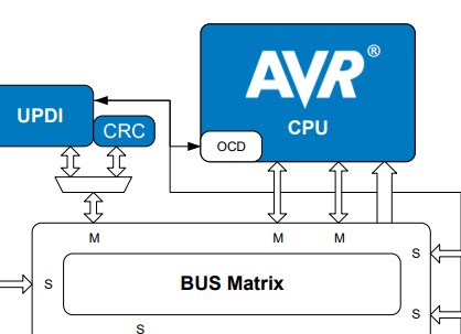 |
The CPU is the brain of the microcontroller where program instructions are executed. It performs arithmetic, logic, control, and data processing operations. It's the central hub for managing the flow of information in the microcontroller. | The arrows connecting the CPU to the bus matrix indicate that the CPU can issue commands and process data from any connected peripheral through this communication backbone. |
2. Identify and distinguish the different types of memory within the microcontroller and their specific uses.
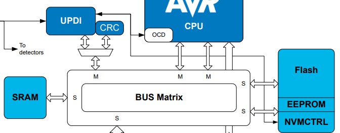 |
SRAM, or Static Random-Access Memory, provides quick access memory for the CPU's operation, primarily used for storing variables and temporary data during program execution. This type of volatile memory requires power to maintain the stored information, meaning that its contents are lost when the device is powered down.
Flash memory, another form of non-volatile memory, contains the program code that the microcontroller executes. Unlike SRAM, flash memory retains its contents even when the power is turned off, which is crucial for storing the firmware that defines the device's behavior. It's commonly used for the long-term retention of the device's operational program. EEPROM, or Electrically Erasable Programmable Read-Only Memory, is also non-volatile and used for persistent storage that can be rewritten. It is often employed to store configuration parameters or small amounts of data that must persist between resets and power cycles, such as calibration data or user preferences. The Non-Volatile Memory Controller (NVMCTRL) manages the reading, writing, and erasure of the flash memory and EEPROM. It ensures safe and reliable access to these memory types, particularly important during firmware updates or when data must be preserved during low-power states. NVMCTRL also often provides security features to protect the contents of non-volatile memory from unauthorized access. Common usages for these memories span from everyday consumer electronics to complex industrial control systems, where the integrity and persistence of program code and data are paramount. |
The data flow arrows between the SRAM and the bus matrix illustrate a two-way communication channel. The CPU accesses the SRAM via the bus matrix for temporary data storage and retrieval. It writes data to SRAM through the bus matrix when storing variables and reads from SRAM when it needs to use these variables for computations. Arrows from the Flash memory to the bus matrix, and from the bus matrix to the CPU, indicate that the CPU fetches its program instructions from the Flash memory through the bus matrix. This design allows the CPU to execute code stored in Flash memory efficiently. Similarly, the EEPROM is connected to the bus matrix with two-way arrows, which means that the CPU can read from and write to the EEPROM through the bus matrix. This is where non-volatile data is stored and persists even when the device is powered down. The Non-Volatile Memory Controller (NVMCTRL) is also connected to the bus matrix with arrows pointing both to and from the Flash and EEPROM. This indicates that the NVMCTRL manages the operations of these non-volatile memory types by interfacing with the bus matrix. It controls the programming, erasure, and protection of the memory contents, ensuring that when the CPU updates firmware or application data, it does so in a manner that is secure and minimizes wear on the memory cells. |
3. Comprehend the microcontroller's clock system, its sources, and how it affects the operation of the device.
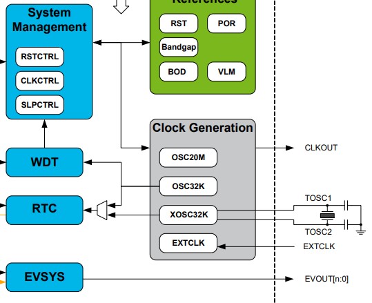 |
Clock generation refers to the process of generating and distributing clock signals within the microcontroller to synchronize its operation and enable the execution of instructions and tasks. On the other hand, RTC refers to a specific functionality or peripheral within the microcontroller that provides real-time tracking of time and date, typically using a low-frequency clock source (such as the 32 kHz oscillator) to maintain accurate timekeeping even in low-power or standby modes.
OSC20M: This represents the internal 20 MHz oscillator, which serves as a high-frequency clock source for the microcontroller's operation. It is commonly used as the main system clock for executing instructions and driving internal processes. OSC32K: This symbolizes the internal 32 kHz oscillator, which provides a low-frequency clock source for low-power operations and timing-sensitive tasks, such as real-time clock (RTC) functionality and low-power sleep modes. XOSC32K: This denotes an external 32 kHz crystal oscillator, which can be connected to the microcontroller to provide a more accurate and stable clock source compared to the internal oscillator. It is often used for RTC applications or other timing-critical tasks. EXTCLK: This represents an external clock input, which allows the microcontroller to synchronize its operation with an external clock signal provided by an external oscillator or clock generator. It provides flexibility for using an external clock source instead of the internal oscillators. |
Connect WDT (Watchdog Timer): The arrow indicates that the clock signal generated by the microcontroller's internal clock sources is provided to the Watchdog Timer module. The Watchdog Timer uses this clock signal to monitor the execution of the microcontroller's program and trigger a system reset if it detects a fault or malfunction, thereby enhancing system reliability and preventing system lock-ups or crashes.
Connect RTC (Real-Time Clock): The clock signal is also supplied to the Real-Time Clock (RTC) module, which maintains accurate timekeeping and date tracking within the microcontroller. The RTC utilizes this clock signal to update the current time and date information, allowing the microcontroller to perform time-sensitive tasks and schedule events based on real-world time. Connect System Management: The clock signal is used by the system management functions within the microcontroller to coordinate various system-level operations, such as power management, clock gating, and peripheral initialization. These functions ensure proper operation and efficiency of the microcontroller's overall system architecture. To CLKOUT: The clock signal may be routed to the CLKOUT pin, which serves as an external clock output for monitoring the microcontroller's clock frequency or providing clock signals to external devices or peripherals. This allows external devices to synchronize their operations with the microcontroller's clock signal. From EXTCLK: The clock signal can be supplied to the EXTCLK input, which allows the microcontroller to synchronize its operation with an external clock source provided by an external oscillator or clock generator. This provides flexibility for using an external clock source instead of the internal oscillators, enabling precise timing control and synchronization in embedded systems. Connect Detectors: The clock signal may also be utilized by various detectors or monitoring circuits within the microcontroller to detect specific events, conditions, or transitions in the system. These detectors may include voltage detectors, frequency detectors, or temperature detectors, which use the clock signal as a reference for their operation. |
4. Analyze the system management functions and their impact on the stability and efficiency of the microcontroller.
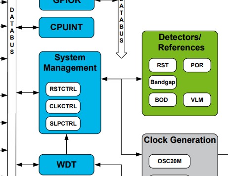 |
System management is critical for the comprehensive oversight of a microcontroller's operation. It encompasses a range of functions designed to ensure efficient and reliable performance. Among these are monitoring power levels, managing energy efficiency through sleep modes via the Sleep Control (SLPCTRL), and ensuring the system's stability through reset operations with the Reset Controller (RSTCTRL). Additionally, system management involves the precise regulation of the microcontroller's clock system through the Clock Control (CLKCTRL). CLKCTRL is pivotal in selecting and managing clock sources, setting the system clock frequencies, and optimizing the clock distribution to the CPU and peripherals | Between the Data Bus and System Management: Arrows to and from the data bus to system management illustrate the dynamic exchange of control signals that regulate data transmission across the system. This bi-directional communication ensures that system management has the necessary oversight to adjust data flow for optimized performance and efficiency, such as reallocating resources or managing bandwidth based on current system demands.
Between Detectors/References and System Management: Arrows to and from detectors/references to system management represent the feedback loop crucial for monitoring system conditions, such as voltage levels, temperature, or external events. These signals enable system management to make informed decisions, adjusting operational parameters or invoking protective measures to maintain system integrity and performance. Between Clock Generation and System Management: Arrows to and from the clock generation to system management encapsulate the control over the system's timing aspects. Through these pathways, system management can alter clock speeds or switch between clock sources, thereby balancing between power consumption and processing needs—a critical function for optimizing energy efficiency without compromising performance. From the Watchdog Timer (WDT) to System Management: Arrows from the WDT to system management signal the watchdog's role in system reliability. If the WDT detects a system anomaly or a failure to reset its timer (indicating a potential software freeze or malfunction), it sends a signal to system management to initiate corrective actions, such as a system reset or entering a safe mode. This ensures the system's ability to recover from errors autonomously, enhancing its robustness. |
5. Examine the serial communication modules (USART, SPI, TWI) and understand their protocols and applications.
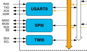 |
USART is used for serial communication between devices and is often used for debugging. SPI is a faster protocol typically used for short-distance communication, while TWI (I2C) is used for communication over a bus with multiple devices. | The bidirectional arrows signify that these blocks can both send and receive data, allowing for two-way communication with other devices in a system. |
6. Delve into the ADC features, such as channel multiplexing, resolution, and sampling rate.
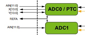 |
The ADC converts analog signals from various sources into digital values that the CPU can process.
ADCO/PTC serves a dual role, functioning as both the output interface for analog-to-digital conversion (ADC mode) and the input interface for touch sensing applications (PTC mode). ADC1 represents an additional analog-to-digital converter module dedicated solely to analog-to-digital conversion tasks. |
Arrows from the ADC block to the CPU and SRAM indicate that the digital data is sent there for processing and potential storage.
AIN: This abbreviation stands for "Analog Input." It denotes that the signals connected to these channels are analog voltages that need to be sampled and converted into digital values by the ADC. [11:0]: This notation specifies the range or number of analog input channels available. The numbers inside the brackets indicate the starting and ending channel numbers. In this case, "11:0" means there are 12 analog input channels in total, ranging from channel 0 to channel 11. X[13:0]" and "Y[13:0]" denote two sets of analog input channels, each with 14 channels. These channels are used to connect external analog signals, such as sensors or voltage sources, to the ADC for conversion into digital values REFA denote Reference voltage A input for the ADC. In ADC applications, a reference voltage is often required to establish the range and accuracy of the conversion process. |
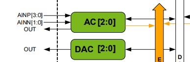
| 7. Explore the Digital-to-Analog Converter(DAC) and Analog Comparator (AC) block, its resolution, and its use in generating analog signals from digital values.
|
The DAC provides the reverse function of the ADC, converting digital values back into a continuous analog signal. This is useful for applications such as sound generation or analog control.
"DAC[2:0]" designation suggests the presence of three individual DACs within the microcontroller. Each DAC can convert digital input values into corresponding analog output voltages. The "AC[2:0]" designation suggests the presence of three individual analog comparators within the microcontroller. Each comparator is capable of comparing two analog input voltages and producing a digital output signal based on the comparison result. |
Arrows emanating from the DAC to the outside world indicate the flow of the generated analog signals to external devices or systems.
AINP[3:0]" and "AINN[1:0]" designations refer to the positive and negative input terminals of each comparator, respectively. The "OUT" designation indicates the output pins or terminals of the comparator block, where the digital output signals are provided. |
8. Investigate the timers and their roles in tasks such as event counting, pulse width modulation, and timekeeping.
 |
Timers are versatile tools within the microcontroller used for measuring time intervals, creating delays, generating waveforms, and scheduling events. They are fundamental to tasks that require precise timing.
16-bit Timer/Counter Type A (TCA) Purpose: The TCA module provides a versatile timer/counter with multiple compare channels and a dedicated period register. It supports various timer modes, including normal, PWM, and frequency generation modes. The TCA timer is commonly used for general-purpose timing, pulse-width modulation (PWM) signal generation, and event capture tasks. 16-bit Timer/Counter Type B (TCB) Purpose: The TCB module comprises two independent 16-bit timer/counter units, each equipped with input capture capability. TCB timers offer flexibility for precise timing measurements, pulse-width modulation (PWM) generation, and event counting tasks. They are commonly used for motor control, sensor interfacing, and other time-critical applications. 12-bit Timer/Counter Type D (TCD) Purpose: The TCD module features a 12-bit timer/counter optimized for control applications. While it may not be explicitly labeled in the datasheet, the TCD functionality is part of the timer resources available in the microcontroller for precise timing and control tasks. It can be used for tasks requiring lower resolution timing or where a separate timer resource is needed. 16-bit Real-Time Counter (RTC) Purpose: The RTC module provides a 16-bit counter specifically designed for real-time clock and calendar functions. It operates using an external crystal oscillator, external clock source, or internal RC oscillator, enabling accurate timekeeping capabilities for time-sensitive applications. The RTC is commonly used for timekeeping, timestamping, and scheduling tasks in embedded systems. |
Arrows to the timers indicate they receive input signals for counting or timing, while arrows from the timers indicate they can trigger other system events or outputs.
TCA0: This stands for Timer/Counter Type A, instance 0. The ATtiny1614, like many microcontrollers, has several timer/counter modules that can be used for a wide range of timing and counting tasks, such as generating PWM (Pulse Width Modulation) signals, measuring time intervals, or counting events. TCA0 is one of these timer/counter modules. WO[5:0]: WO stands for "Waveform Output," and the numbers in brackets [5:0] indicate six channels available for this purpose, numbered from 0 to 5. These channels can be used to output compare signals, which are often utilized in PWM applications. Each channel can generate an output signal based on comparisons between a counter value and a predefined threshold, allowing for precise control over signal timing and waveform generation. WO[A,B,C,D]: Each letter represents a specific channel that can be independently configured. Having multiple channels (like A, B, C, D) allows a single Timer/Counter module to control multiple outputs simultaneously. For instance, you might use one channel to dim an LED while another controls a motor's speed. |
| Understand the watchdog timer's role in system reliability and error recovery. | The watchdog timer serves as a fail-safe mechanism. If the system becomes unresponsive, the WDT can automatically reset the system, helping to recover from software errors or hardware faults. | The arrow from the WDT to the reset line highlights its ability to initiate a reset sequence, restoring normal operation when a system error is detected. |
Analyze the Configurable Custom Logic (CCL) for creating user-defined logic functions without CPU intervention.
 |
The CCL allows designers to create hardware-level logic functions, such as combining input signals and generating output signals based on custom-defined conditions, which can operate independently of the CPU. | The arrows between the CCL and other peripherals indicate that the CCL can interact with multiple system components, receiving inputs from them or controlling them based on logic conditions.
LUTn-IN[2:0]: This notation represents the input channels to a specific Look-Up Table (LUT) within the Configurable Custom Logic (CCL) module, where "n" denotes the LUT instance number (as there can be multiple LUTs within a single CCL module), and "[2:0]" indicates that there are three input channels available for this LUT, labeled as input 0, input 1, and input 2. These inputs can be connected to various internal or external signals, depending on the microcontroller's configuration capabilities. The LUT uses these inputs to perform logic operations based on a predefined truth table. LUTn-OUT: This represents the output of the Look-Up Table "n". After processing the inputs according to its configuration, the LUT produces an output signal based on the logic defined within the LUT's truth table. This output can then be used for further processing within the microcontroller or directed to external pins for interfacing with other devices. |
I7. Reading Datasheet for ATTINY 1614 -- Pin out and Multiplexing
I/O Multiplexing, in the context of microcontrollers like the ATtiny series, refers to the ability of a single pin to serve multiple functions, selectable by the programmer.
| Pin Number | Pin Name | Function(s) | Additional Capabilities |
|---|---|---|---|
| 1 | VCC | Power Supply Voltage | --- |
| 14 | GND | Ground | --- |
| 2-5, 11-13 | PAx | General-Purpose Input/Output (GPIO) | Analog Input (PA0-PA7), PWM Output (PA4-PA7), UPDI (PA0) |
| 6, 7 | PBx | General-Purpose Input/Output (GPIO) | PWM Output (PB0, PB1), Timer Oscillator (TOSC1/PB3, TOSC2/PB2) |
| 8, 9, 10 | PA1, PA2, PA3 | Special/Other | Serial Clock (SCK/PA1), Master In Slave Out (MISO/PA2), Master Out Slave In (MOSI/PA3/RESET) |
| 10 | PA3 | Programming, Debug, Reset | Unified Program and Debug Interface (UPDI) |
| 9 | PA2 | Clock | External Clock Input (EXTCLK) |
| 6 | PB3 | Clock | Timer Oscillator 1 (TOSC1) |
| 7 | PB2 | Clock | Timer Oscillator 2 (TOSC2) |
I8. Reading Datasheet for ATTINY 1614 -- Memory
Flash Memory is where the program code is stored. With 16 KB available, it limits the complexity of the program that can be run.
SRAM (Static Random Access Memory) is used for temporary data storage during program execution, with 2 KB indicating how much data can be handled in real-time.
EEPROM (Electrically Erasable Programmable Read-Only Memory) retains data even when power is off. With 256B and a specific number of write/erase cycles, it informs how data like device configuration can be stored and for how long.
I/O memory Space encompasses all memory addresses used for accessing and controlling hardware peripherals and devices. It compromises of I/O registers and I/O memory.
I wanted to know how to use programming to access the specific address, but chatgpt did not have anything useful. Microchip have a AVR Assembler which was not written for begineers like me.
one can control the fuse bit to lock the chip.
if a memory map starts at address 0x00 and a register is located at offset 0x05, it means that the register is located 5 bytes into the memory region starting at address 0x00. Therefore, the absolute address of the register would be 0x00 + 0x05 = 0x05.
DEVICEIO01,2,3 identifies the device, SERNUM0-9 to distinguish uC, TEMPSENSE0,1 store correction factors for temperature measurements from the onchip sensor., OSC16ERR3V stores the signed oscillator frequency error value relative to the nominal oscillator frequency when
running at an internal 16 MHz at 3V, as measured during production.
Watchdog Configuration register (WDTCFG) is a special register within the microcontroller's memory space. It stores configuration settings related to the watchdog timer, which is a hardware feature designed to reset the microcontroller if certain conditions are not met within a specified time period.
While the Watchdog Configuration register may not be part of the traditional RAM or ROM memory, it is still considered memory in the broader sense because it stores data or configuration settings that are used by the microcontroller during operation. It falls under the category of memory because it is accessed and manipulated by the microcontroller's CPU during program execution.
Brown out Detection(BOD) register controls configuration settings related to brown-out detection, which is a feature that monitors the supply voltage of the microcontroller and resets it if the voltage drops below a certain threshold, preventing erratic behavior or data corruption.
Timer counters(eg TCD0CFG) are commonly used in microcontrollers for tasks such as generating time delays, measuring time intervals, or controlling the timing of various operations. It also helps parameters such as fault detection modes, fault actions, or fault sources for the Timer Counter Type D peripheral.
System Configuration 0 register (SYSCFG0) have three config options.
1. CRC Source (CRCSRC):
Determines the source for CRC calculations.
Options include calculating CRC for different sections of Flash memory or disabling CRC altogether.
Reset Pin Configuration (RSTPINCFG):
2. Configures the functionality of the Reset/UPDI pin.
Options include configuring it as a GPIO pin, a UPDI pin, or a traditional RESET pin.
3. EEPROM Save During Chip Erase (EESAVE):
Controls whether EEPROM memory is preserved or erased during a chip erase operation.
Options include preserving EEPROM data or erasing it along with the rest of the chip.
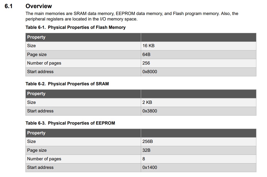
| Specification | ATTINY1614 | Arduino Uno (ATmega328P) | Implications for Prototyping |
|---|---|---|---|
| Flash Memory Size | 16 KB | 32 KB | The smaller Flash on the ATTINY1614 means less space for code, requiring more efficient programming. It is where your code is residing. You use LD to load memory and ST to store data to memory. One can also use LPM to load memory into the register
Signature bytes 1,2,3 which contains informations that identify the chip is stored in the flash. |
| SRAM | 2 KB | 2 KB | Equal SRAM sizes mean similar capabilities for runtime operations and data handling. It is voltatile so noramlly used to store variables and data structures. |
| EEPROM (Electrically Erasable Programmable Read-Only Memory) | 256 Bytes | 1 KB | With less EEPROM, the ATTINY1614 can store fewer configuration settings or persistent data.
EEPROM is often used for storing user preferences, calibration values, and other persistent data The EEPROM is controlled by the Nonvolatile Memory Controller (NVMCTRL). it also contain firmware settings inside EEPROM, there is a setting known as "user row" It is a section of memory that is reserved for storing user-defined data or settings. |
I9. Reading Datasheet for ATTINY 1614 -- CPU Architecture
CPU architecture refers to the design framework that defines the structure and operation of a computer's central processing unit (CPU). This includes the specifics of how a CPU processes information, executes instructions, and interacts with other components of the computer system.
| Component / Term | Description and Functionality | Flow / Interaction Details |
|---|---|---|
| Register File (R0 - R31) | The Register File consists of 32 x 8-bit general-purpose registers (R0-R31) which provide flexible, fast access for operations. R26-R31 have special functions as pointer registers (X, Y, Z) for indirect address or pointer operations. | Data can move bi-directionally between these registers and the ALU. The ALU processes data using these registers and the results can be stored back into them. Additionally, data from these registers can be stored to or retrieved from the Data Memory. |
| Program Counter | The Program Counter (PC) is crucial for the sequential execution of instructions, holding the address of the current or next instruction that the CPU will execute. The PC increments after each instruction fetch, or can be modified by jump and branch instructions. | The PC is connected to the Flash Program Memory, dictating which instruction should be fetched next. After an instruction is executed, the PC increments or changes according to control flow instructions (like jumps or branches). |
| Flash Program Memory | This is a non-volatile memory module where the machine code of a program is stored. It retains the program code even when the power is off, making it essential for embedded systems like microcontrollers. | The content of the Program Counter points to a specific location in Flash Program Memory, from which the Instruction Register fetches the next instruction to be decoded and executed. |
| Instruction Register | The Instruction Register temporarily holds the next instruction fetched from the Flash Program Memory, waiting to be decoded. It is a critical intermediary that captures the raw instruction data. | The fetched instruction is held in the Instruction Register and then passed to the Instruction Decode block, where the binary instruction is translated into signals that control other parts of the CPU. |
| Instruction Decode | It deciphers the binary code in the Instruction Register to determine what actions the CPU should perform, like which register to access or which operation to execute in the ALU. | Once the instruction is decoded, the necessary control signals are generated and sent to the ALU and other components to carry out the instruction. The Instruction Decode process dictates the flow of data between the Register File, ALU, and Data Memory. |
| Stack Pointer | The Stack Pointer (SP) is a special-purpose register that points to the current top of the stack in the Data Memory. The stack is used for temporary storage of addresses and data during procedure calls, interrupts, and CPU internal operations. | The SP adjusts itself during push (store) and pop (retrieve) operations on the stack, which occur in the Data Memory. It increments or decrements depending on whether data is being added to or removed from the stack. |
| Status Register | This register contains various status flags that are affected by the ALU operations. For instance, a zero flag indicates that the result of the last operation was zero; a carry flag indicates an overflow from the most significant bit during addition, etc. | The Status Register is updated based on the results of operations performed in the ALU. It also affects decision-making in the CPU, such as conditional branching where the execution path changes depending on the status flags. |
| ALU (Arithmetic Logic Unit) | The ALU is the CPU's calculator, capable of performing arithmetic operations (like addition and subtraction) and logic operations (like AND, OR, NOT). It's where the actual computation of data occurs. | The ALU receives operands from the Register File, performs the requested operation, then sends the result back to the Register File or to the Data Memory. It also updates the Status Register based on the outcome of its computations. |
| Data Memory | Data Memory is where the CPU stores or retrieves data that is not currently being processed by the CPU. It contains RAM for variable data, along with I/O registers and control registers for interfacing and controlling peripherals. | Data Memory interacts with nearly all other components: it stores results from the ALU, maintains the stack with the help of the Stack Pointer, and can serve as a source or destination for data in the Register File. It is a central point for data storage and retrieval during operation. |
| Multiplexer (Trapezium Symbols), but the data sheet seems to call it multiplers | Multiplexers in a CPU architecture diagram are control devices that take multiple input signals and select one to pass through as the output. They direct the flow of data within the CPU, ensuring the correct data path is followed according to the operation being performed. | In this CPU architecture, the multiplexers are likely responsible for selecting between different data sources to be sent to the ALU, for example, choosing between immediate values, register file contents, or results from other operations. They are controlled by the Instruction Decode logic, which determines the source of the data based on the current instruction. |
Theory for DataSheet - Not Required
Types of Memory in Embedded Systems
Embedded systems use various types of memory for different purposes, each with its advantages and limitations. This table explains each memory type, including its size on the Arduino Uno, purpose, pros and cons, common applications, and relevance to the Arduino Uno.
| Memory Type | Purpose and Pros/Cons | Common Applications | Relevance in Arduino Uno |
|---|---|---|---|
| SRAM (Static RAM) | Size: 2KB. Temporary storage for data and program execution. Pros: Fast access. Cons: Volatile, data lost on power off. | Variable storage during program execution. | Used for storing variables; efficient use is crucial due to limited size. |
| Flash Memory | Size: 32KB. Non-volatile storage for program code. Pros: Retains data without power. Cons: Limited write cycles. | Storing application code. | Stores sketches; important to manage size for complex programs. |
| EEPROM | Size: 1KB. Used for storing small amounts of data that must survive power cycles. Pros: Data can be rewritten. Cons: Limited write cycles. | Storing configuration settings. | Useful for data that must persist between sessions, like user settings. |
| ROM (Read-Only Memory) | N/A for direct user access in Arduino Uno. Stores firmware that doesn't change. Pros: Non-volatile. Cons: Not directly accessible for programming. | Firmware storage, bootloaders. | Contains the bootloader; not directly used in Arduino programming. |
Types of Peripherals in Embedded Systems
Embedded systems utilize a variety of peripherals for interfacing with the external world, executing specific tasks, and expanding capabilities. This table outlines these peripherals, their roles, common uses, and associated pins on the ATmega328P microcontroller:
| Peripheral Type | Purpose | Common Applications | ATmega328P Pins |
|---|---|---|---|
| Digital I/O | Reads and writes digital values. | Button inputs, LED outputs. | Ports D0-D13 |
| Analog Input (ADC) | Converts analog signals to digital values. | Sensor data reading, analog signal processing. | A0-A5 |
| PWM Output | Generates analog output signals via pulse-width modulation. | Motor control, LED dimming. | D3, D5, D6, D9, D10, D11 |
| UART | Facilitates serial communication between devices. | Serial monitors, PC or microcontroller communication. | RX (D0), TX (D1) |
| SPI | Enables high-speed synchronous serial data transfer. | SD cards, displays, other SPI devices. | SS (D10), MOSI (D11), MISO (D12), SCK (D13) |
| I2C | Allows two-wire serial communication. | Sensor modules, EEPROM, LCDs. | SDA (A4), SCL (A5) |
| Counters/Timers | Measure time intervals or count events. | Scheduling tasks, measuring time, generating delays. | Various, integrated into MCU function |
| Analog Comparator | Compares two analog voltage levels and outputs a digital signal based on the comparison. | Battery monitoring, sensor signal processing. | A6 (AIN0), A7 (AIN1) - Note: Actual pins for comparators might vary or require setup in software. |
| Digital to Analog (DAC) | Converts digital values to analog signals. | Audio output, analog signal generation. | N/A for ATmega328P |
Word Size in Embedded Systems
The word size in computing and embedded systems refers to the number of bits processed by the system's processor in a single operation. It significantly impacts the system's processing power, memory efficiency, and overall performance. This table provides an overview of various word sizes, their purposes, and applications:
| Word Size | Purpose | Common Applications |
|---|---|---|
| 8-bit | Used for simple control applications where low power consumption and cost are more critical than processing speed. | Microcontrollers for home appliances, toys, and other consumer electronics. |
| 16-bit | Offers a good balance between processing power and cost, suitable for applications requiring moderate computation and data processing. | Automotive control systems, smart sensors, and small-scale embedded devices. |
| 32-bit | Provides high processing power and memory addressability, ideal for complex applications with extensive computational needs. | Smartphones, multimedia devices, and advanced embedded systems requiring significant data processing. |
| 64-bit | Enables access to vast amounts of memory and enhances performance for data-intensive applications. | High-end computing devices, servers, and systems dealing with large datasets or requiring high-speed data processing. |
Processor Families in Embedded Systems
Think of embedded systems like the brains in many toys and gadgets around us. These brains are made up of tiny parts called processors. Just like we have different types of toys for different games, there are different types of processor families for different jobs in gadgets. Here’s a little guide on which brain to pick for your toy or gadget:
| Processor Family | When to Use | Important Points |
|---|---|---|
| AVR (like in Arduino) | Use it when you're making something small and not too complicated, like a light that turns on with a clap! | It’s easy to use, perfect for beginners, and great for school projects. |
| ARM Cortex | When your toy needs to be smart, like a robot that can walk and talk, pick ARM Cortex. | It can do many things at once and is used in lots of smart gadgets. |
| MSP430 | If your gadget needs to run a long time on a tiny battery, like a watch or a step counter, this is a good choice. | It uses very little power, so your battery lasts longer. |
| ESP32 | Use ESP32 when your gadget needs to talk to the internet, like a weather station that tells you if you need an umbrella. | It’s good at using Wi-Fi and Bluetooth to connect to the internet and other gadgets. |
| PIC Microcontrollers | When you're making something that controls lots of things at once, like a big model train set, PIC can be your friend. | They are very versatile and can be used in many different types of projects. |
Embedded Languages and Key Concepts in Embedded Systems
This table dives into the languages and concepts crucial to embedded systems programming, explaining each and highlighting their relevance to Arduino Uno projects.
| Term | Explanation | Relevance in Arduino Uno |
|---|---|---|
| Assembly Language | A low-level programming language that's close to the computer's machine language. | While Arduino sketches are written in C/C++, understanding Assembly can help optimize critical sections for performance. |
| GCC (GNU Compiler Collection) | A compiler system supporting various programming languages, turning source code into executable programs. | The Arduino IDE uses avr-gcc, a version of GCC, to compile sketches into machine code the Arduino Uno can run. |
| Makefiles | Files containing a set of directives used by a make build automation tool to generate a target/goal. | Not directly used in the Arduino IDE, but understanding makefiles is beneficial for advanced Arduino programming and custom builds. |
| Toolchains | A set of programming tools used in sequence to create executable programs from source code. | The Arduino software includes a toolchain (compiler, assembler, etc.) specific to AVR microcontrollers, like the one in Arduino Uno. |
| Memory Leaks | A scenario where a program continuously consumes memory without releasing it, leading to exhaustion of available memory. | Arduino Uno has limited SRAM; careful management is necessary to prevent memory leaks in long-running applications. |
| Memory Overrun | Occurs when a program writes data outside the allocated memory space, potentially overwriting other data. | Can cause program crashes or unexpected behavior on the Arduino Uno, especially with buffer overflows in data handling. |
| Race Conditions | A condition where the system's behavior depends on the sequence or timing of uncontrollable events. | Relevant in multitasking scenarios or when using interrupts on the Arduino Uno, requiring careful synchronization. |
| Interpreters | Software that directly executes instructions written in a programming or scripting language without requiring them to be compiled. | While Arduino sketches are compiled, understanding interpreters is useful for integrating scripts or other interpreted languages with Arduino projects. |
In-System Development in Embedded Systems
Embedded systems often require programming and debugging directly within the hardware they reside in. This is crucial for developing, testing, and maintaining the firmware that controls various devices. Here’s a closer look at the tools and protocols used for in-system development, explained with technical clarity and simple analogies for better understanding:
| Development Tool | Purpose and Explanation | Common Applications | Technical Analogy |
|---|---|---|---|
| JTAG (Joint Test Action Group) | A protocol for debugging and programming embedded systems, allowing developers to inspect and manipulate the processor's state and memory. | Complex embedded systems, automotive ECUs, telecommunications. | Like a multi-tool (Swiss Army knife) for engineers to 'talk' to the device's brain. |
| SWD (Serial Wire Debug) | A two-pin alternative to JTAG for ARM microcontrollers, simplifying connection for programming and debugging. | ARM-based microcontrollers, IoT devices. | Using a simplified, efficient walkie-talkie (instead of a bulky satellite phone) for communication. |
| UPDI (Unified Program and Debug Interface) | A single-wire programming and debugging interface for newer AVR microcontrollers. | Latest AVR microcontrollers like ATtiny series. | A direct, one-on-one chat line (like a secure direct message) for updates and checks. |
| ISP (In-System Programming) | Enables programming of microcontrollers after being placed in a circuit, without needing special debug hardware. | AVR, PIC microcontrollers, and others where removing the microcontroller is impractical. | Updating a toy's (device's) instructions without taking it apart, using a standard USB cable. |
Operating Systems, Clocks, and Serial Communication in Embedded Systems
In the realm of embedded systems, operating systems play a crucial role in managing resources, while clocks determine the pace at which operations are performed, and serial communication facilitates data exchange. Let's explore these concepts further:
| Concept | Purpose and Explanation | Common Applications |
|---|---|---|
| ROS (Robot Operating System) | A flexible framework for writing robot software. It provides tools and libraries to simplify the task of creating complex and robust robot behavior across a wide variety of robotic platforms. | Robotics research, industrial automation, and educational robots. |
| FTDI (Future Technology Devices International) | A company that produces chips for converting USB communication to serial communication, enabling devices with serial ports to be connected to computers via USB. | USB to serial adapters, development boards, and programming hardware. |
| Serial Port | Allows for serial communication, where data is transmitted one bit at a time, over a communication channel or computer bus. | Device management, sensor data collection, and debugging interfaces in embedded systems. |
| Instruction Cycle | The process by which a computer retrieves a program instruction from its memory, determines what actions the instruction dictates, and carries out those actions. This cycle is fundamental to the operation of any CPU. | Central to the functioning of microcontrollers and CPUs in all computing devices, from simple embedded systems to complex computers. |
| Overclocking | Increasing the clock rate of a computer to exceed that certified by the manufacturer, speeding up the instruction cycle. This can lead to improved performance but also increased heat and potential instability. | Used by enthusiasts to enhance performance in computing devices, though less common in embedded systems due to thermal and reliability concerns. |
Comparison of Performance and Development Workflow
When choosing a microcontroller for a project, it's important to consider both its performance capabilities and the development workflow it supports. Here’s how the Arduino Uno R3, Xiao ESP32 C3, and ATTINY1614 stack up:
| Microcontroller | Architecture | Performance | Development Workflow | Common Use-Cases |
|---|---|---|---|---|
| Arduino Uno R3 | AVR (ATmega328P) | Lower clock speed (16 MHz), suitable for basic tasks and learning purposes. | Arduino IDE for easy programming and large community support. Simple USB connection for programming. | Educational projects, simple robotics, DIY electronics. |
| Xiao ESP32 C3 | RISC-V | Higher performance with faster clock speeds and more cores, supports Wi-Fi and Bluetooth connectivity. | Support for Arduino IDE and Espressif IDF, providing flexibility for beginners and advanced users. Requires installation of additional board support packages. | IoT devices, wireless applications, advanced robotics. |
| ATTINY1614 | AVR | Good performance for its size, with a wide operating voltage range and low power consumption. | Can be programmed via UPDI. Supports Arduino IDE with an external programmer, suited for projects where size and power consumption are critical. | Wearable devices, smart sensors, small-scale automation projects. |
Comprehensive Overview of ATMEGA328P Microcontroller Specifications
This enhanced overview delves into the ATMEGA328P microcontroller's specifications, providing explanations of technical terms for beginners and illustrating how to utilize these features in coding.
| Specification | Detail and Beginner Explanation | Relevance in Embedded Systems | Accessing via Code |
|---|---|---|---|
| Microcontroller Architecture | 8-bit AVR. This means the brain of the microcontroller processes data in 8-bit chunks, which is like reading only 8 letters at a time. | Perfect for simple to moderately complex tasks where balancing speed and power consumption is important. | Defined at the time of setting up your development environment and by choosing the correct microcontroller/board type. |
| Operating Voltage Range | 1.8V to 5.5V. This is the range of electricity levels the microcontroller can safely work with. | Allows the microcontroller to be used in various projects, from low-power wearable devices to more power-intensive applications. | N/A - This parameter is related to hardware design rather than directly accessed via code. |
| Clock Frequency | Up to 20MHz. Similar to the heart rate, this frequency determines how fast the microcontroller can execute tasks. | Higher frequency means the microcontroller can do its job faster, useful for tasks requiring quick responses. | Use the prescaler function in your code to adjust operation speed, within the limits set by hardware. |
| Flash Memory | 32KB. Think of this as the microcontroller's long-term memory, where your program is stored. | More Flash memory allows for more complex programs to be stored, enabling more sophisticated operations. | Managed by the IDE during program upload; no direct code manipulation required. |
| SRAM | 2KB. This is the short-term memory for temporary data created and used by your program. | Essential for running programs that require data storage and manipulation on the fly. | Variables declared in your program use SRAM. Managing variable size and quantity can optimize usage. |
| EEPROM | 1KB. EEPROM is like a notebook for the microcontroller, where data can be written and saved even when the power is off. | Useful for saving settings or states that need to be remembered between restarts or power-offs. | Accessed through EEPROM library functions like EEPROM.write(address, value) and EEPROM.read(address). |
| Digital I/O Pins | 23. These are like the microcontroller's fingers, allowing it to interact with sensors, buttons, LEDs, etc. | Enables the microcontroller to control and communicate with a wide array of external devices. | Use pinMode(pin, mode) to set as INPUT or OUTPUT, digitalWrite(pin, value) for output, and digitalRead(pin) for input. |
| Analog Input Channels | 6. These pins can read varying signals, not just ON or OFF but any value in-between, like how bright a light is. | Crucial for projects needing to measure continuous quantities, such as temperature or light levels. | Use analogRead(pin) to read the voltage at a pin, translating it into a value between 0 and 1023. |
| Communication Interfaces | UART, SPI, I2C. These are like different languages the microcontroller can speak to communicate with other devices. | Allows for versatile connections to sensors, displays, and other microcontrollers for data exchange. | Accessed using specific libraries or commands in your code, like Wire.begin() for I2C, or SPI.begin() for SPI communication. |
| Interrupts | External and Internal. Interrupts are like a tap on the shoulder, telling the microcontroller to pay attention to something immediately. | Enables responsive designs that can react promptly to external events, improving efficiency. | Use attachInterrupt(digitalPinToInterrupt(pin), ISR, mode) to configure and respond to interrupts. |
The ATMEGA328P serves as a robust foundation for embedded system projects, offering a rich feature set for a wide range of applications. By understanding and leveraging these specifications through coding, developers can create highly functional, reliable, and efficient designs.
Key Specifications of ESP Microcontrollers
This section is prepare for younger children reading the datasheet, it outlines crucial information about ESP microcontrollers, such as the ESP8266 and ESP32, highlighting why these features matter for creating smart devices and projects in the world of embedded systems.
| Feature | Explanation | Why It's Important |
|---|---|---|
| Wi-Fi Capability | Allows the microcontroller to connect to the internet wirelessly. | This means your projects can send or receive information from the internet, like weather data or controlling lights from your phone. |
| Bluetooth (ESP32) | A wireless technology for exchanging data over short distances. | Enables your gadgets to communicate with other Bluetooth devices, such as speakers or smartphones, making them smarter. |
| CPU Cores and Speed | How many brains (cores) the chip has and how fast they think (speed). | More cores and higher speed mean your device can think faster and do more tasks at once, like a mini-computer. |
| Memory | Storage space for the microcontroller to remember things (programs and data). | More memory lets your device remember more instructions and data, making it capable of doing more complex jobs. |
| GPIO Pins | General Purpose Input/Output Pins - like the hands and feet of the microcontroller. | They let your device interact with the outside world, like turning on lights, reading temperature sensors, or controlling motors. |
| ADC (Analog to Digital Converter) | Converts analog signals (like sound or light levels) into digital data the microcontroller can understand. | Important for projects that need to measure real-world phenomena, such as light intensity or temperature. |
| Power Consumption | How much electricity the microcontroller uses. | Lower power consumption is key for battery-powered projects, making them last longer before needing a recharge. |
ESP microcontrollers are like tiny brains that allow you to create amazing gadgets that can interact with the world through the internet or Bluetooth, sense the environment, and control other devices. Their powerful features are why they're so popular in projects and products that need to be smart and connected.