4. PCB Production
Group Assignment
G1. Group Assignment- Electronic Board Production
Attached is the link to group assignment
Individual Assignment
0. Instructors Suggestions
To Add why did I use FR4:- I wanted to try different materials. According to internet, FR4 have better thermal, mechanical, and electrical properties and FR1 is cheaper.
To fix:
- add either board layout (.brd) or svg/png for the board that you milled and link to it. --- 6 May, placed in JSOn for EasyEDA Designer and .
- include arduino sketch & link to it --- 6 May, Updated Broken link.
- "Useful Theory 1" - complete or remove --- 6 May, Deleted and Followed Instructor suggestion to place advance concepts at my work.
Checklist
- ☑ Linked to the group assignment page -- Done
- ☑ Documented how you made (mill, stuff, solder) the board --Done
- ☑ Documented that your board is functional --Done
- ☑ Explained any problems and how you fixed them --finger Injury, surface mount compounds are outsource to vendor
- ☑ Uploaded your source code --Done
- ☑ Included a 'hero shot' of your board -- inserted pictures.
I1. Individual Assignment- Electronic Board Production
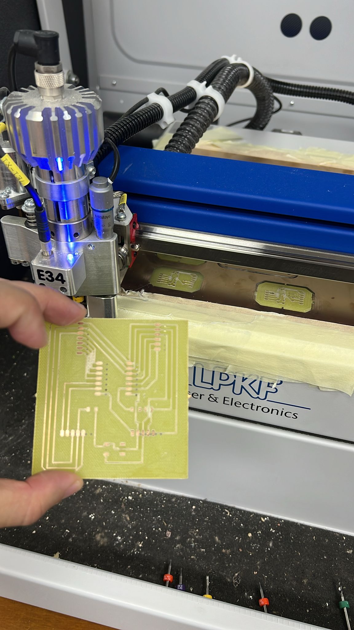
I followed the process of PCB production based on the theories discussed earlier. This overview outlines the steps I took. Due to a medical condition that hinders my PCB soldering skills for surface mount components, I completed all milling processes but required external help for the soldering of smaller components.
| Process | Description |
|---|---|
| Mounting FR4 | I secured the FR4 material using double sided tape onto the machine bed to ensure stability during the milling process. |
Import PCB Design into LPKF 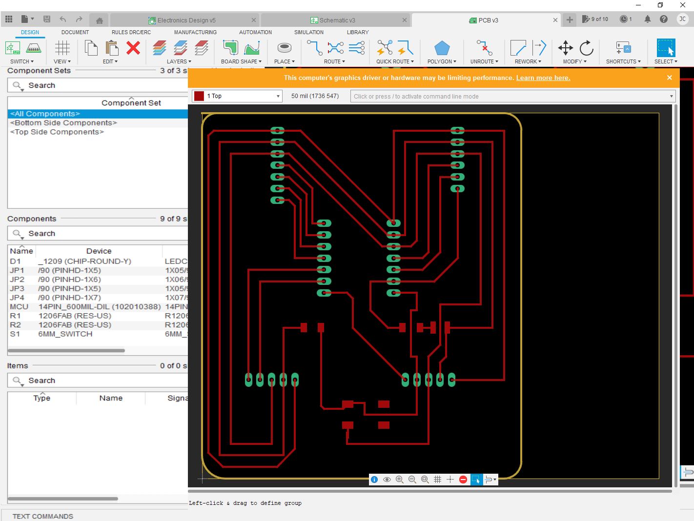
|
I transferred the PCB design files into the LPKF milling machine's software for production. |
Assign Layers to the Design 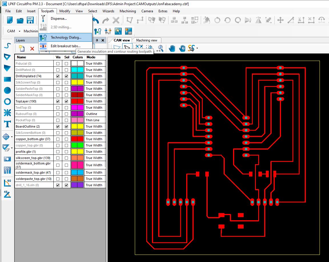
|
I specified which layers of the PCB design to mill and drill. |
Placement of Design and Adjust Settings 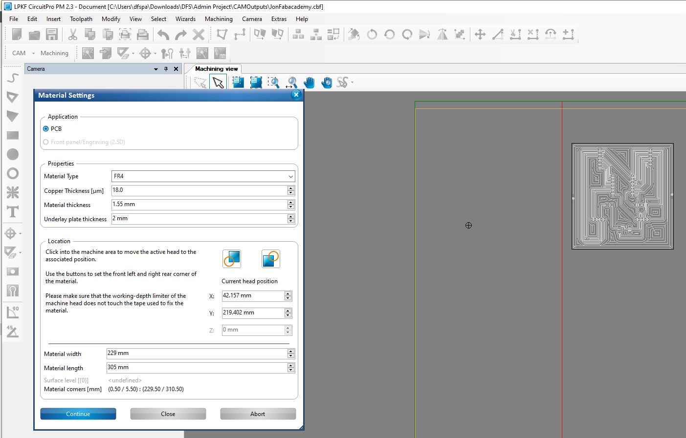 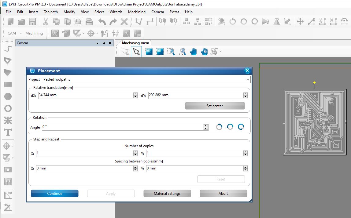
|
I adjusted the position of the design on the FR4 material and configured machine settings for optimal milling. |
Generate Toolpath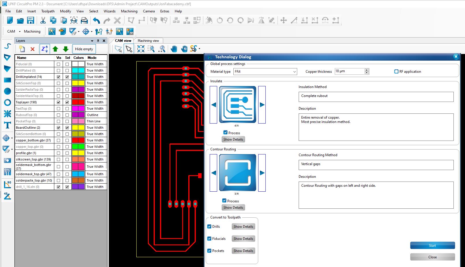 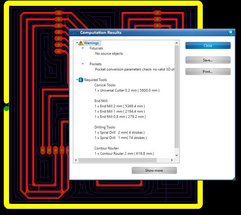
|
I created path that the milling tool will follow to remove material and create the PCB layout. |
Change Bits when Prompted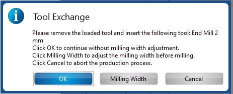
|
I switched out milling bits as required by the design's complexity and the milling stages. |
Cut off the Milled Piece
|
I removing the completed PCB from the remaining FR4 material after milling is finished. |
Solder the Parts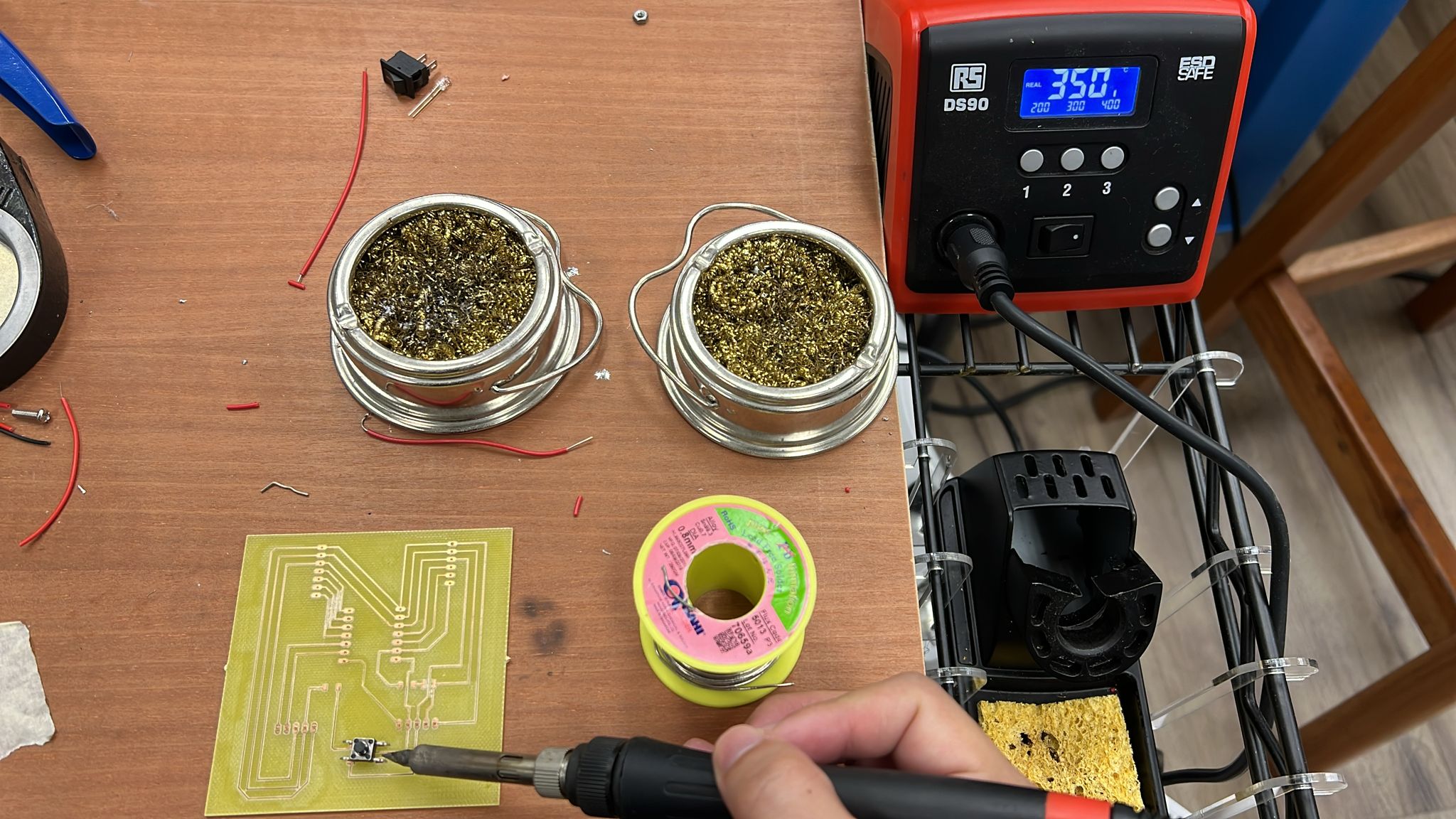
|
Attaching electronic components to the PCB through soldering, applicable for components I was able to solder. |
Send to Outside Experts for Soldering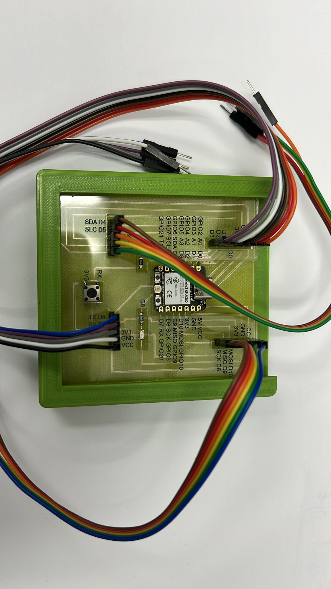
|
Due to my medical condition, surface mount components requiring precision soldering were sent to professionals. |
I2. Individual Assignment- ESP32-C3 Xiao Programming
This section outlines the steps necessary to program the ESP32-C3 Xiao module using the Arduino IDE.
| Action | Details |
|---|---|
| Install Arduino IDE | I downloaded and installed the latest version of the Arduino IDE from the official Arduino website. |
Add ESP32 Board Support
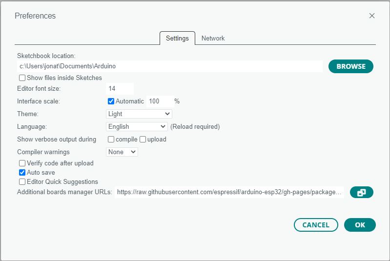 |
I opened the Arduino IDE, navigated to File > Preferences, and add the ESP32 boards manager URL to the Additional Board Manager URLs field. The URL can be found on the official Espressif GitHub or Seeed Studio documentation for the ESP32-C3. |
Install ESP32 Board Package
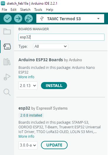 |
Went to Tools > Board > Boards Manager, searched for "ESP32", and installed the latest version of the ESP32 by Espressif Systems. |
Select Your Board
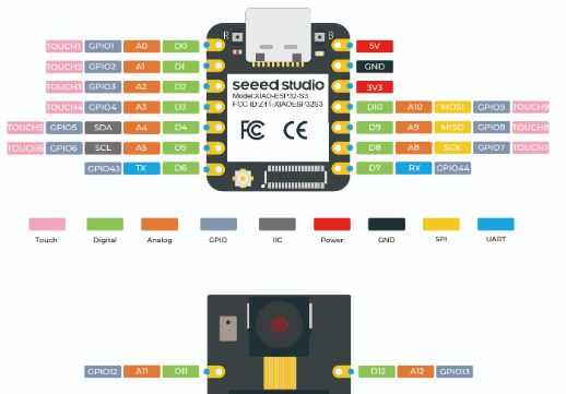 |
Under Tools > Board, navigated to the ESP32 Arduino section and selected the Seeed Studio Xiao ESP32-C3 board. Mine was Xiao_ESP32C3, Note: choosing the wrong module will cause error during pin assignment. |
Choose COM Port
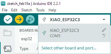 |
I connected my ESP32-C3 Xiao to my computer via USB. Then selected the correct COM port under Tools > Port. |
Prepare Code
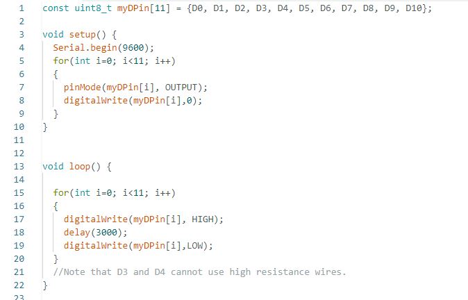 |
I Wrote my code in the Arduino IDE. The code which I wrote allows me to check all the pins of the Microcontroller |
Compile and Upload
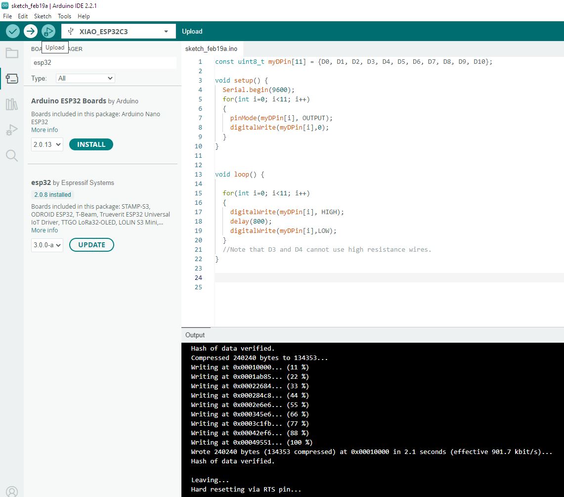 |
I clicked the "Upload" button in the Arduino IDE to compile code and upload it to the ESP32-C3 Xiao. I ensured that no errors are present in the compilation and uploading process. |
| Verify Operation
|
Once the code is uploaded, I monitored the ESP32-C3 Xiao's output for all the 11 pins. |
I2. Basic Workflow of PCB Design to External Production
The PCB design and production process encompasses conceptualization, schematic design, layout creation, and component selection. Following this, the design undergoes validation to ensure functionality and performance. Gerber files are then generated for manufacturing, where PCBs are fabricated and components are assembled. Thorough testing is conducted to verify functionality and reliability before deployment in the intended application. This structured workflow guarantees the production of reliable and efficient PCBs for a variety of electronic devices and systems. The pictures shown below are the steps I took for this assignment
| Step | Description |
|---|---|
1. Conceptualization 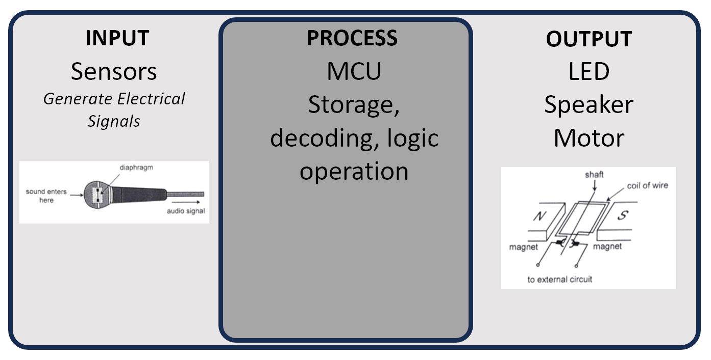 |
I started with define the requirements and specifications of the PCB design, including functionality, size, and electrical connections. I Identified the key components and features. Normally For Singapore Secondary Students, they start with the block diagram shown on the left. |
2. Schematic Design 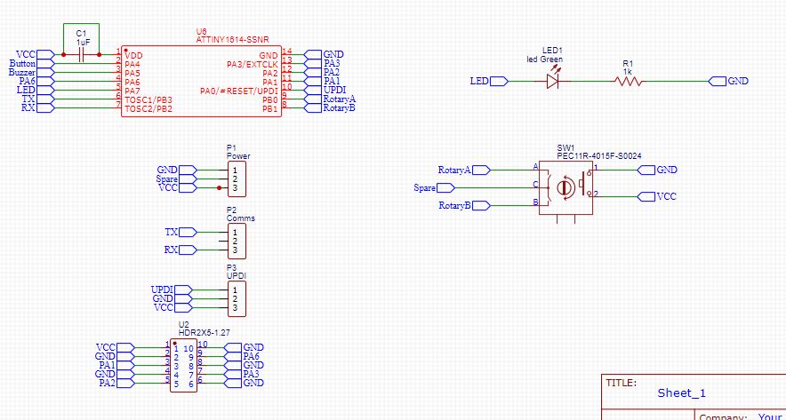 |
I create a schematic diagram of the PCB layout, depicting the connections between components using symbols and nets. I designed the circuit topology and define signal paths. Beside is the picture of schematic Design, I made using EasyEDA |
3. Component Selection 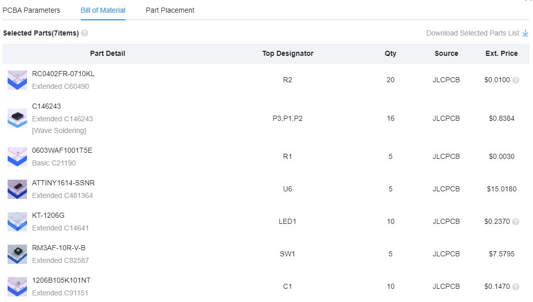 |
I Chose electronic components (such as resistors, capacitors, and integrated circuits) based on the schematic design and project requirements. Consider factors such as cost, availability, and performance. Beside is the picture of Bill of materials in schematic design |
4. PCB Layout Design 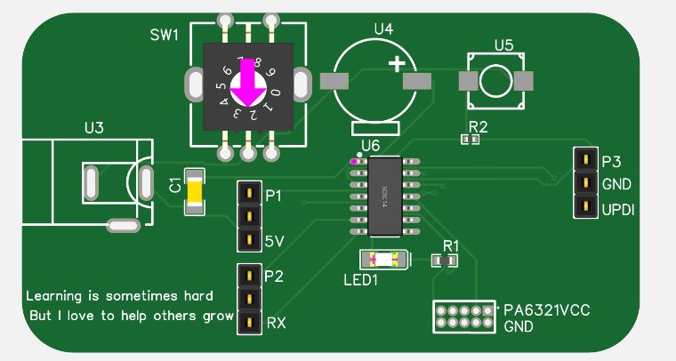 |
I translated the schematic diagram into a physical layout of the PCB, arranging components and traces on the board surface. i ignored signal integrity, power distribution, and thermal management as they are not significant considerations in this project. The picture shows the layout of my PCB components |
5. Routing 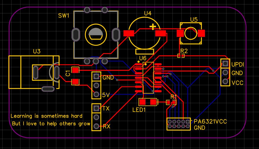 |
I routed electrical connections (traces) between components on the PCB layout. This picture shows the route |
6. Design Validation 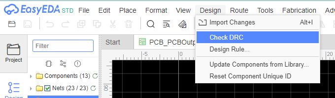 |
I checked for errors, such as electrical shorts, open circuits, and design rule violations. I used Design Rule Checks in EasyEDA |
7. Gerber File Generation 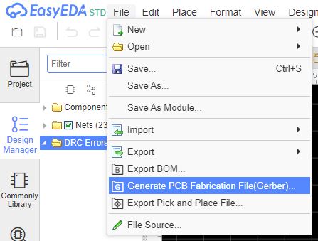 |
I generated Gerber files containing the PCB layout information, including copper layers, solder mask, and silkscreen layers. Gerber files are used by PCB manufacturers to fabricate the physical PCB. I exported the Gerber File using this feature |
8. Manufacturing 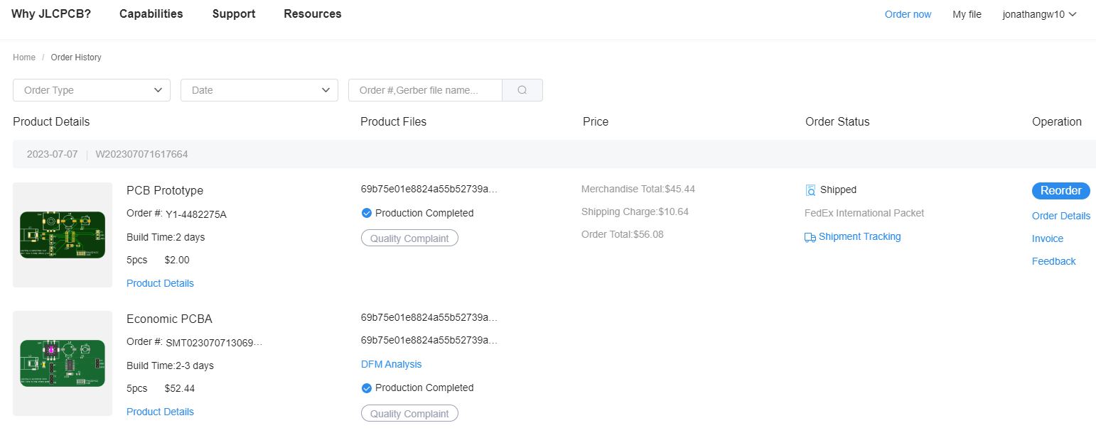 |
I Sent the Gerber files to a PCB manufacturing facility for fabrication. PCBs are typically manufactured using processes such as etching, drilling, and solder mask application. I used JLPCB as onboard production house. |
9. Assembly 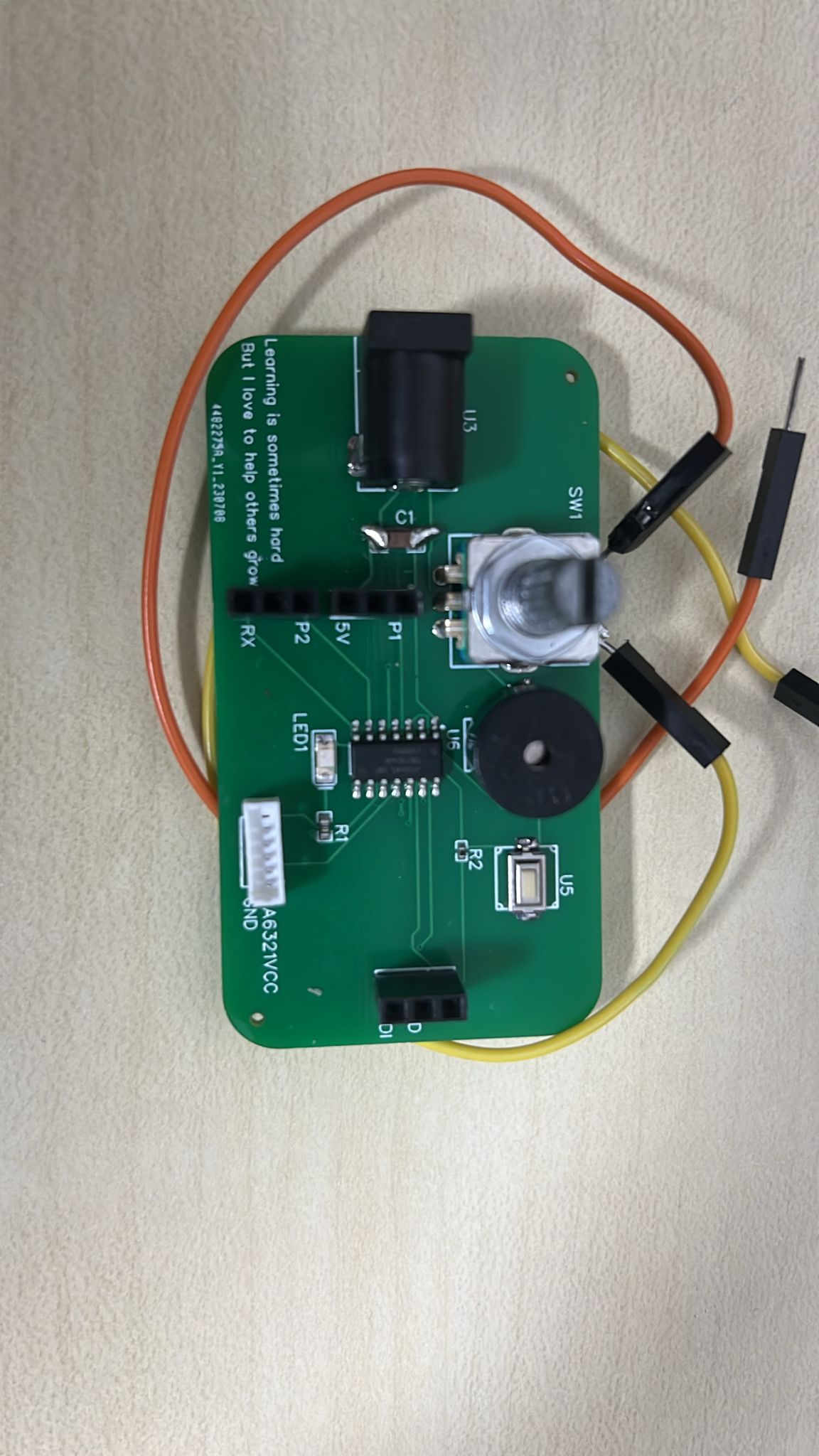 |
I assembled the missing components and send for local vendors to do soldering |
| 10. Testing | I tested the assembled PCB for functionality, performance, and reliability. Use testing equipment (multimeter continuity test) and coded procedures to verify proper operation and identify any defects or issues. |
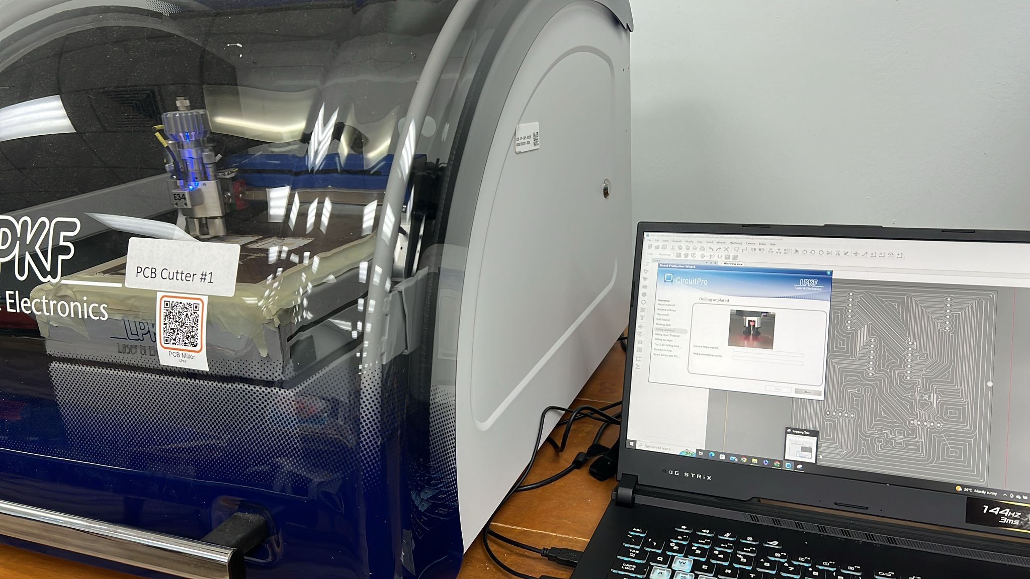
I3. Converting Gerber Files to Toolpaths at LPKF
Converting Gerber files into toolpaths at LPKF is a crucial step in the PCB manufacturing process, ensuring accurate milling operations based on the PCB design specifications. The process involves several detailed steps:
| Step | Description |
|---|---|
| 1. File Import |
i Began by importing the Gerber files into LPKF's software platform. Ensure that all necessary layers, including copper traces, solder mask, and silkscreen, are correctly imported. I Verified that the files are aligned and accurately represent the PCB design. |
2. Layer Configuration 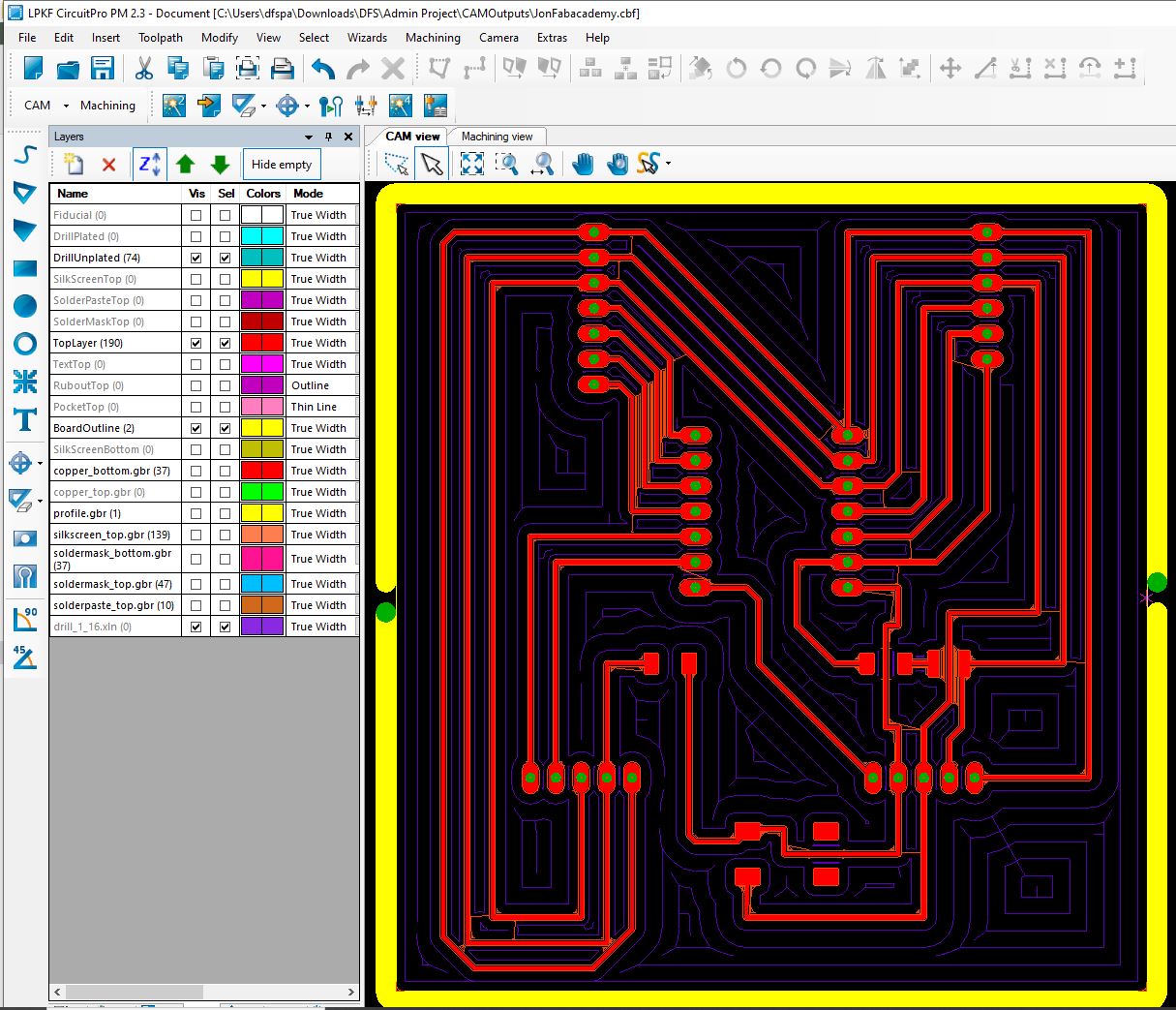 |
I configured each imported layer according to the desired milling parameters. Specified tool diameters, milling depths, and clearance settings based on the PCB design requirements. Adjust layer settings to account for different materials and thicknesses used in the PCB stack-up. |
| 3. Toolpath Generation
|
Using LPKF's CAM software, I generated toolpaths based on the configured layer settings. The software calculates the milling paths required to remove copper material and create PCB traces, pads, and features. |