11. Output devices
This weeks task was to produce output to LCD display.
Group assignment:
- Probe an input device(s)’s analog and digital signals
-
Document your work to the group work page and reflect on your individual page what you learned
-
Here is the link to the current version of the group documentation for this week.
-
I learned from the group work that the current requirements of the LCD board is remarkable compared to the currenct consumption of the MCU system selected itself. I also had to think how to connect the cables to the multimeter we use here in order to measure the current.
Individual assignment:
- Measure something: add a sensor to a microcontroller board that you have designed and read it.
Learning outcomes
- Demonstrate workflows used in sensing something with input device(s) and MCU board
Have you answered these questions? - Linked to the group assignment page
-
Documented what you learned from interfacing an input device(s) to microcontroller and how the physical property relates to the measured results
-
Documented your design and fabrication process or linked to previous examples.
-
Explained the programming process/es you used
-
Explained problems and how you fixed them
-
Included original design files and source code
-
Included a ‘hero shot/video’ of your board
I2C signalling
I2C, short for inter-ic, is “a synchronous, multi-controller/multi-target (controller/target), packet switched, single-ended, serial communication bus.”(Wikipedia)
In this weeks assignment I2C signaling is used to interface the LCD panel control board to the ATtiny412 microcontroller board
I2C is a synchronous serial bus. I2C physical layer consists of two bidirectiona open-collector or open drain lines. It has SDA (serial data line) for transmiittin data and SCL (serial clock line) for synchronisation. SDA line is bidirectional, SCL clock is provided by the bus master device of the bus.
The pinout of ATtiny 412 are shown in the image below.
In the ATtiny412 microcontroller, the SDA and SCL signals are connected to pins
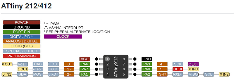
SDA is connected to PA1 and SDL is connected to PA2. When looking at the circuit board layout of the MCU, it can be seen that PA1 is connected to the Pin 5 of board connector J2 and PA2 is connected to the Pin 4 of the connector J2. These signals should be connected to the corresponding lines in the connected I2C device.
I2C has 7-bit address space. The messages can be sent to an address. In the LCD controller case there are three open jumpers, A0,A1 and A2 for setting the device address. In case of using only one LCD controller module, there is no need to change the address and the default address of 0x27 can be used.
In our case, when the address of the I2C LCD controller is known, the LCD library takes care of the communications between the host (MCU) and the registers of the connected I2C device (the LCD controller board). The LCD controller board will then send commands and data to the LCD display.
More information of I2C signaling in Arduino can be found here
Description of I2C signals needed and where to connect them in ATtiny412 etc.
Design of the interface board
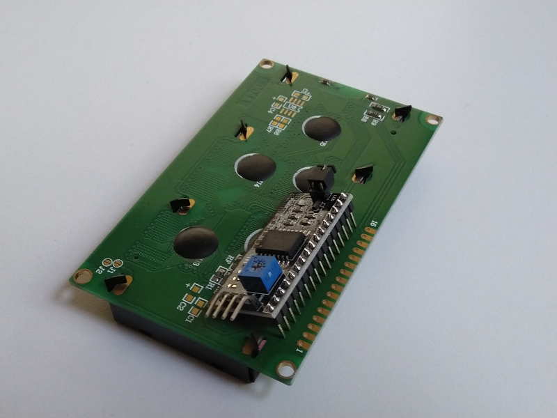
We were given a LCD board and an interface board for the LCD board. Our task was to interface the board to the MCU card we designed earlier.
Back of the LCD module and the intefdace board:
LCD display board front view including the pinout in the upper edge of the module:
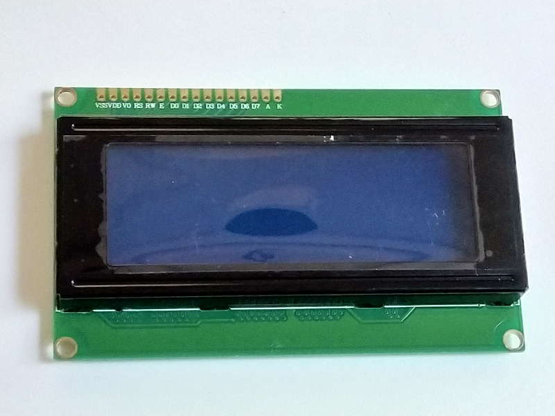
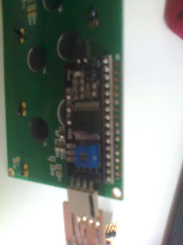
The LCD control board pinout is shown in the image below. Note the pinout of the control board and open jumpers for changing the board address. Blue potentiometer can be used to change the contrast of the display.
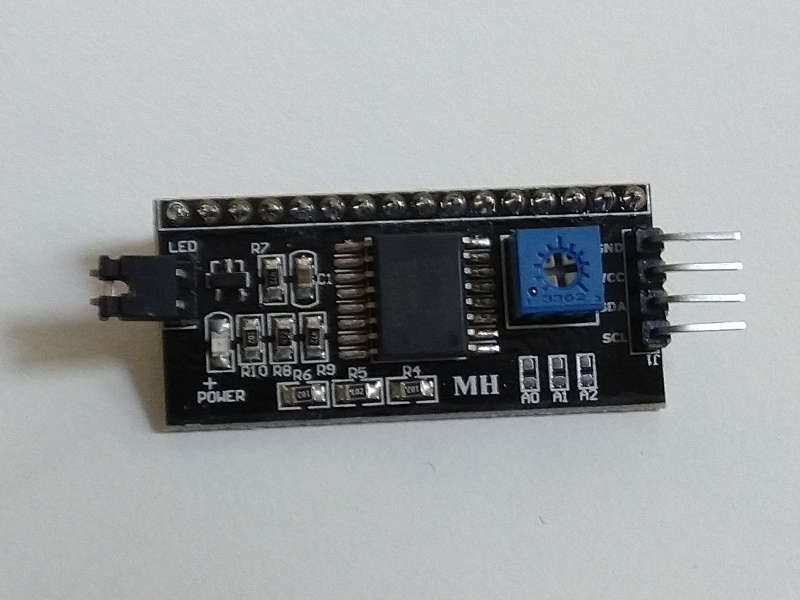
The pinout of the control board from up do down is GND (ground), VCC (positibe terminal of the power input), SDA (I2C data line) and SCL (I2C serial clock line).
Unfortunately the pinout of the LCD display adapter board differs from the pinout of the MCU board designed previously, so an interface board is required. It was suggested, that the three wires required would look untidy and making a robust enough cable would require the same amount of work than making the circuit board. Also, reconnecting the board is easier with the adapter card.
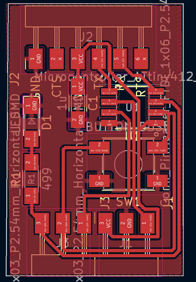
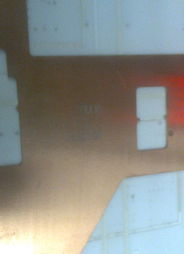
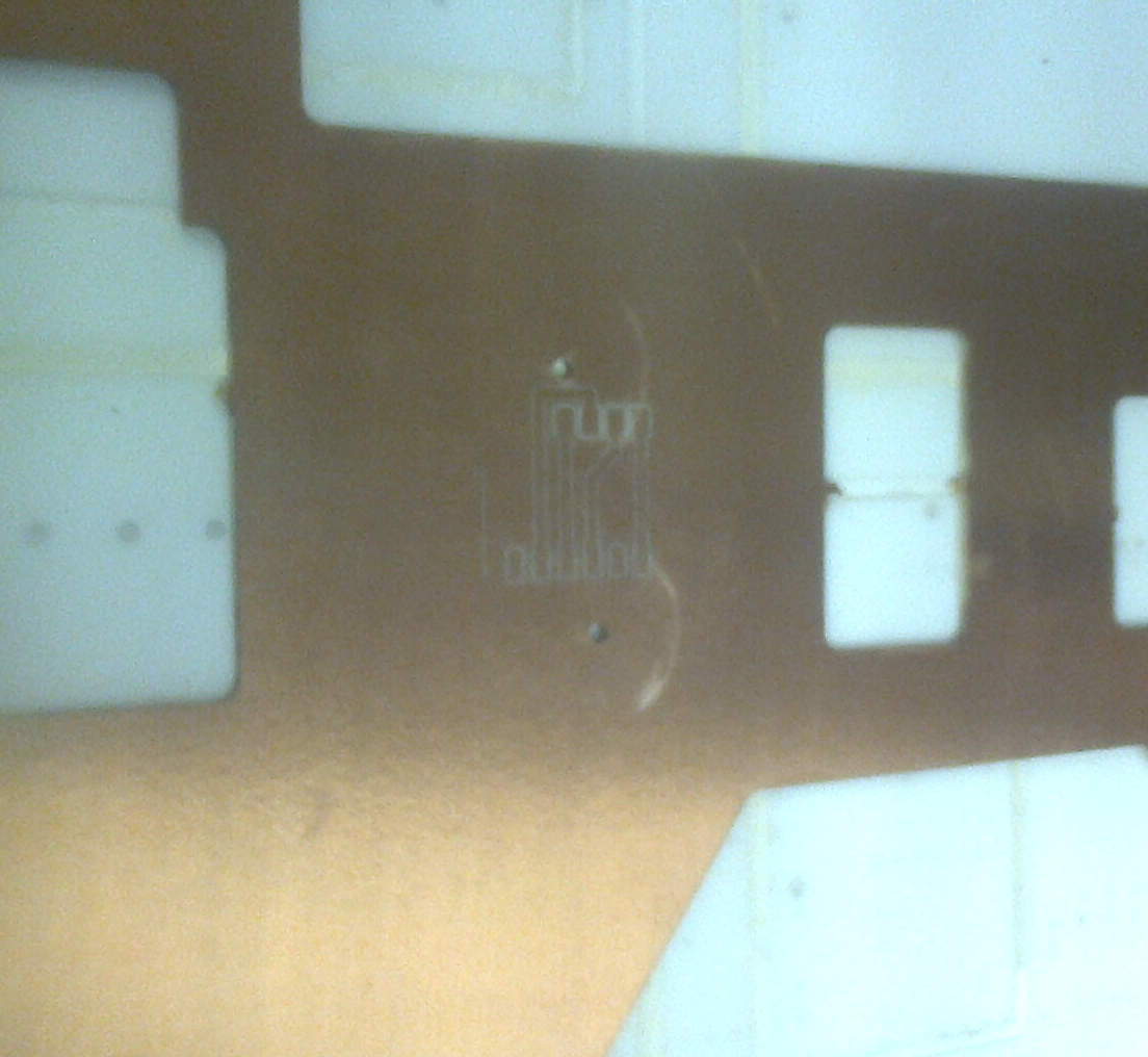
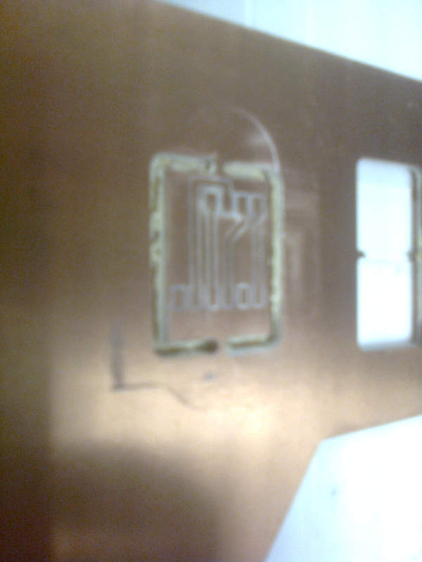
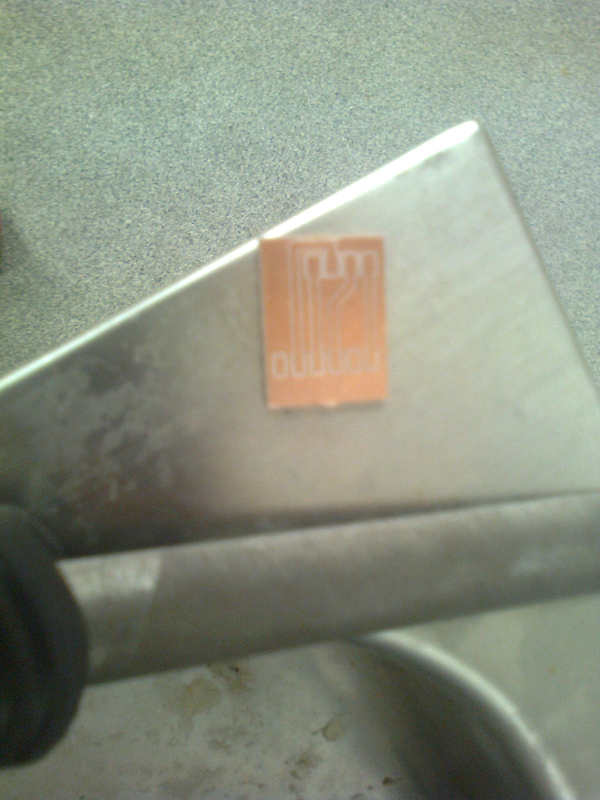
The layout for an interface board was designed in KiCad. I have a previous ecample how to produce a circuit board on Electronics design week documentation. With such a simple board it is faster to go directly to layout editor and do the design by skipping the schematic part.
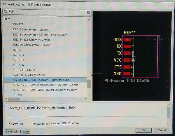
The components (2 connectors, PinHeader_1x04 and PinHeader_FTDI_01x06) were selected from the Fablab library.
 )
)
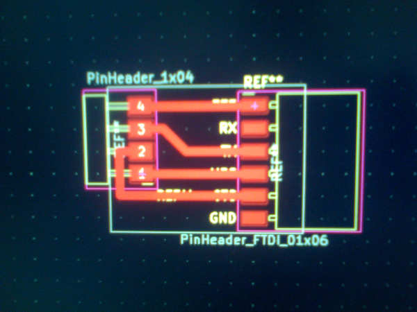
The traces were drawn on F.Cu layer with Route Tracks and the Edge.Cuts edge was drawn with Draw a rectangle.
The traces were drawn in order to match the pinouts od the LCD control module and the controller board. The pin headers are of different size and the pin order does not match. Making the circuit board is more robust design and helps later when using the display and microcontroller modules in the Final Project.
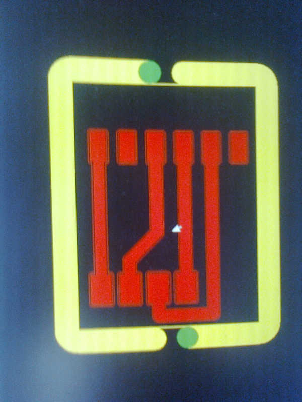
The circuit layout is shown in the image below.
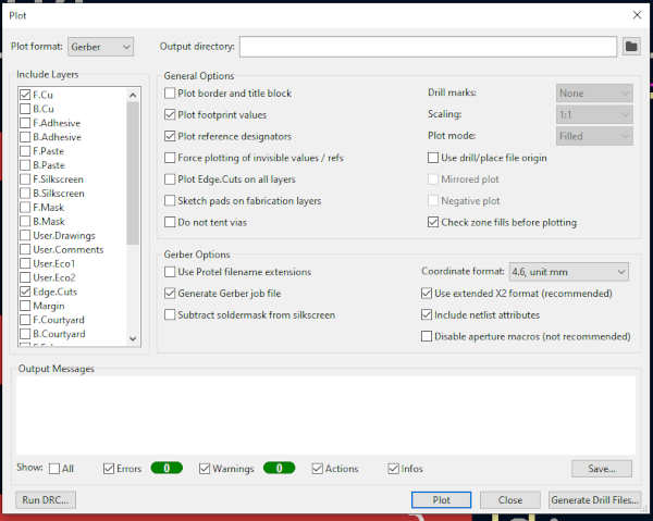
The designed layout was then plotted.
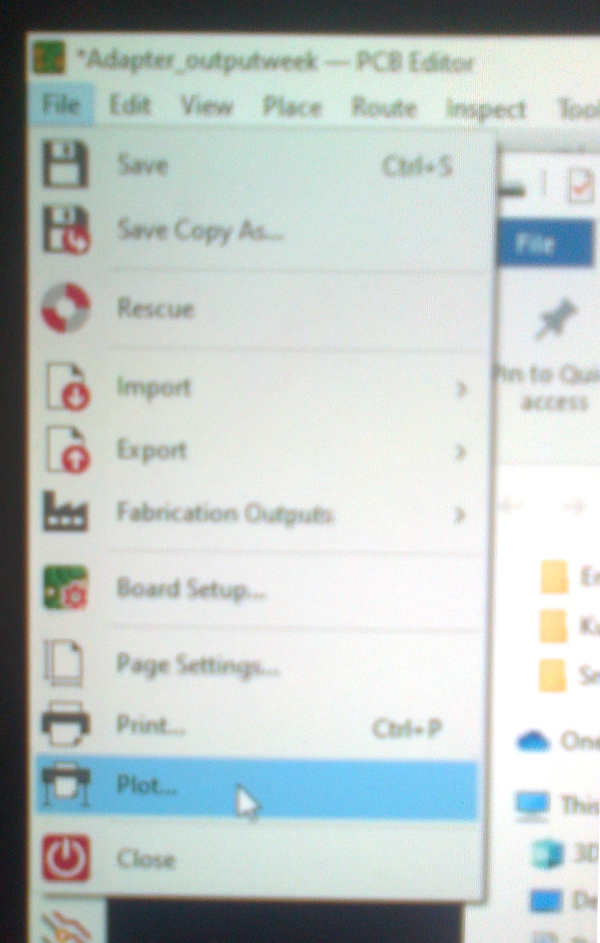
F.Cu and Edge.Cuts were selected on the plots and Plot was pressed.
I started the milling program.
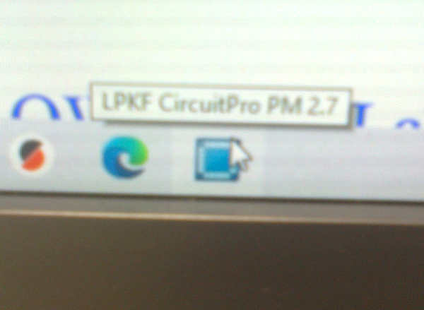
LPKF CircuitPro PM 2.7 program was started.
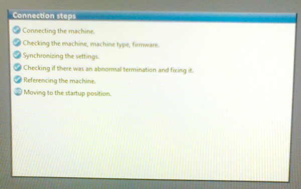
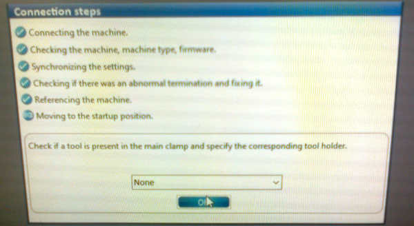
After the program had connected the milling machine, I clicked ok.
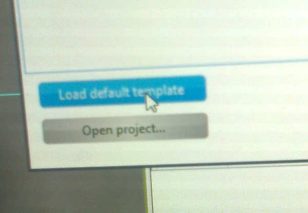
Then I loaded the default template.
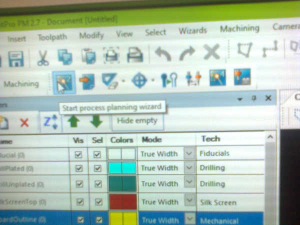
Then I started the Process planning wizard.
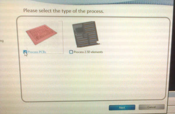
I selected Process PCBs as the process type.
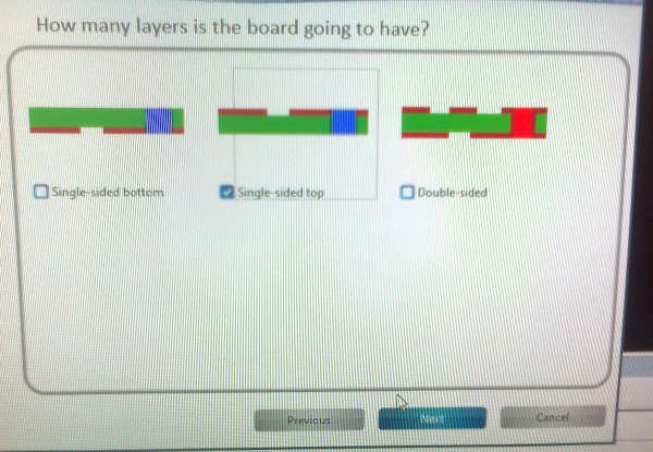
I chose 1 layer board as a board type.
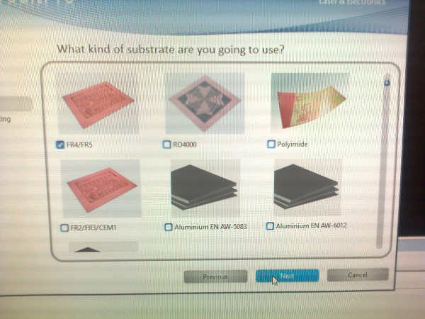
I chose FR4 as a substrate type.
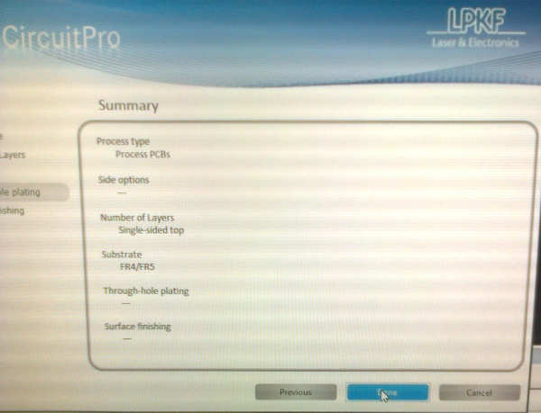
The summary concluded this section of the planning wizard.
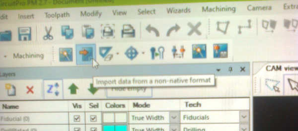
I started the Input data from a non-native format wizard.
At this point, I corrected the “select F.Cu and Edge.Cuts” step in plotting the file and then continued.
I opened the Edge_Cuts and F_Cu files.
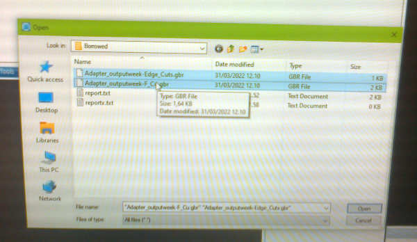
The image looked familiar, so I pressed OK.
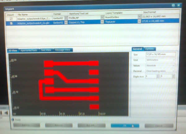
Layout with outline looked good as well. This concluded this wizard.
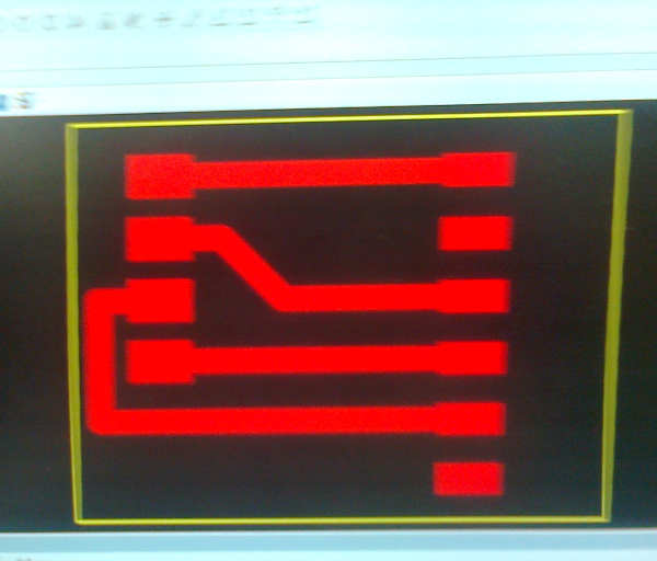
Then I selected Generate isolation and contour routing toolpath-wizard.
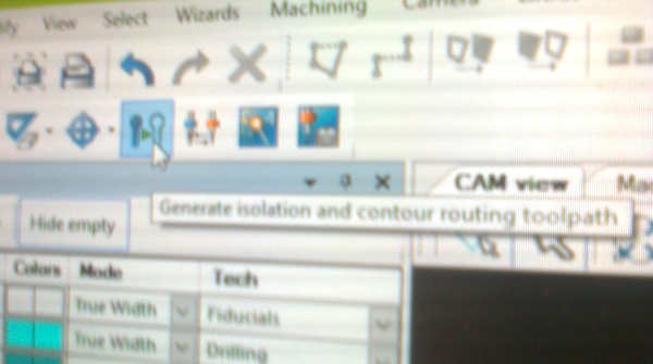
I selected the countour routing.
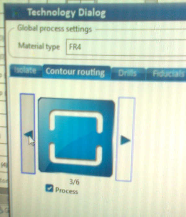
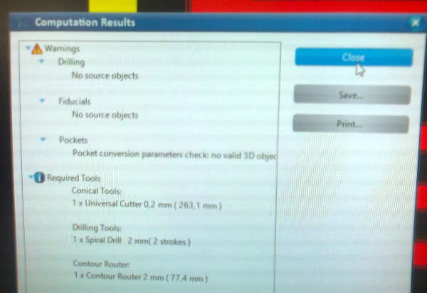
I got some warnings about the missing drilling source objects. That was ok.
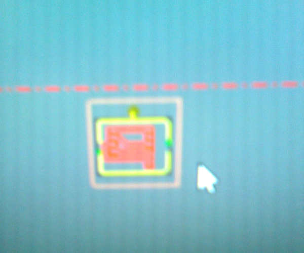
The layout and the contours looked fine.
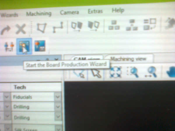
Then I started the board production wizard.
The program asked to fasten the circuit board material.
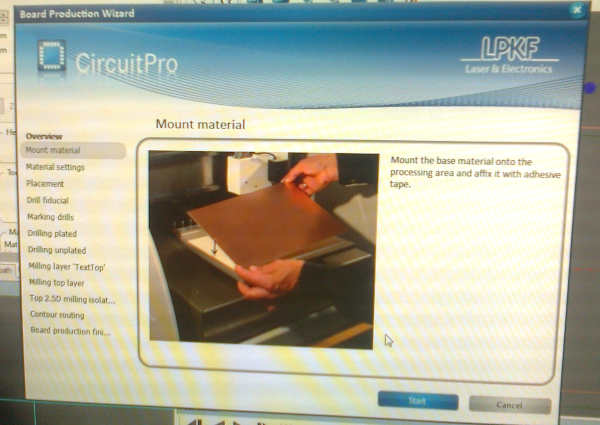
The circuit board material was fastened with tape.
The material settings window was the next phase.
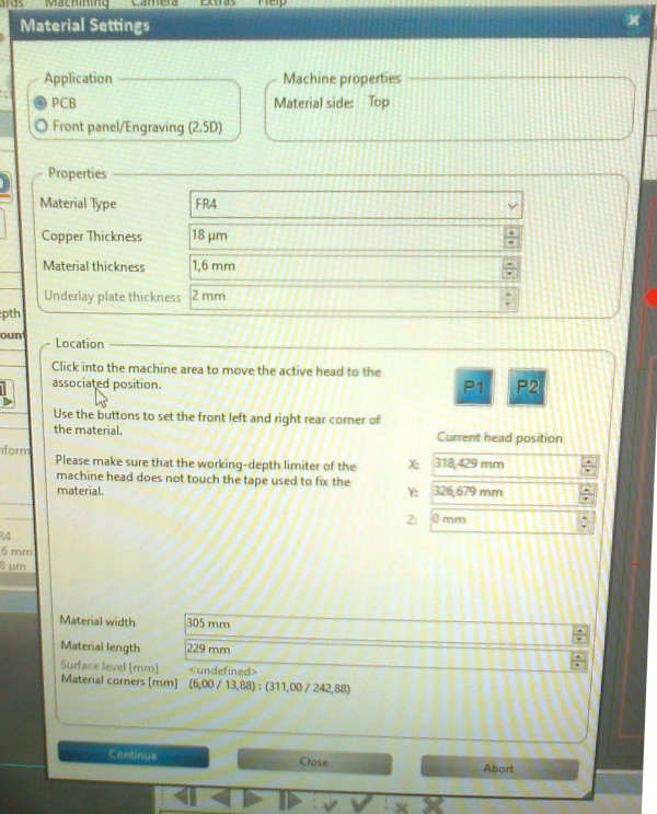
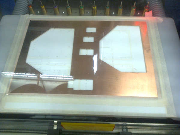
The copper thickness was adjusted to 35 mm and the area on the circuit board used for the milling, as well as the placement of the layout on the area were set.
When selecting the area, it was important that the black “ring” where the tool will be placed should be over copper. P1 cornerpoint for the milling area was selected here.
P2 cornerpoint for the milling area was selected here.
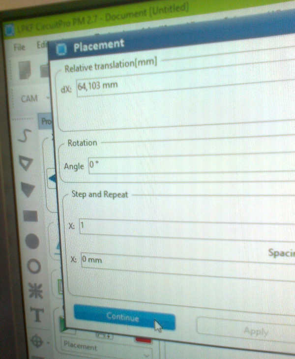
The layout was dragged inside the selected milling area.
Continue was selected for the placement.
The progress was saved.
The program asked, if measuring the milling width was neccessary.
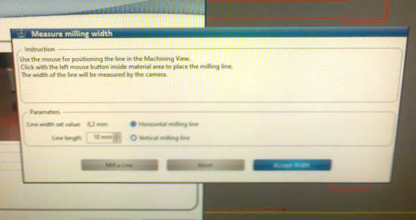
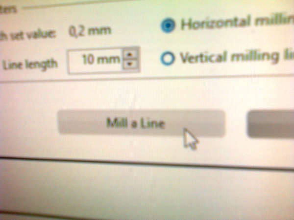
Mill a line was selected.
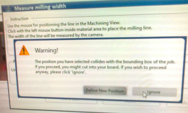
I selected a position for milling. It was quite close to the layout, so a warning was show. I ignored it.
The line width could have been better, but was accepted for this purpose.
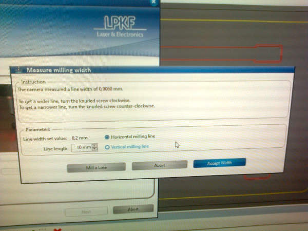
I selected accept width.
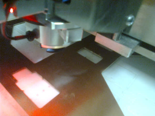
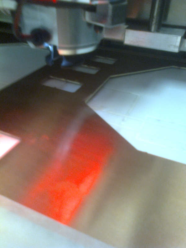
When the milling began, the layout was milled on the selected area.
For the separation, holes were milled first.
Then the area was almost cut out as selected.
When the milling was ready, the tapes were removed, fiber glass dust was removed with a vacuum cleaner and the board was washed. Then I removed the taps with a proper tool.
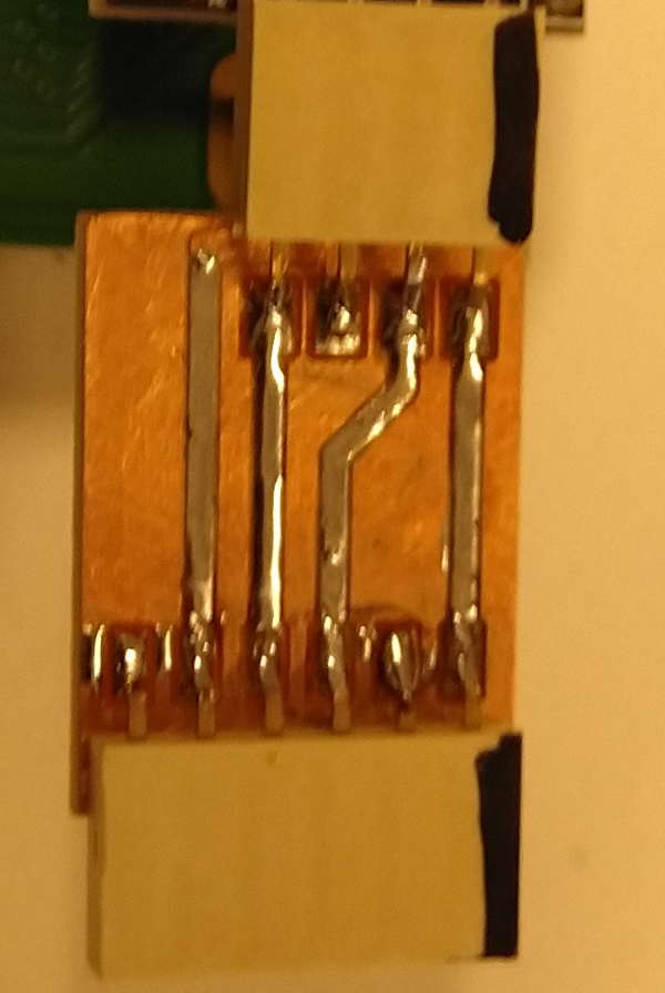
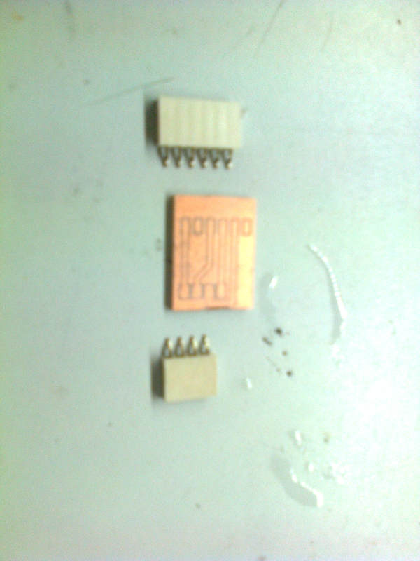
The connectors were found and the board was ready for soldering. The soldering phase was uneventful. I used flux and a lot of material for mechanical support.I also soldered the control ic to the display.
 )
)
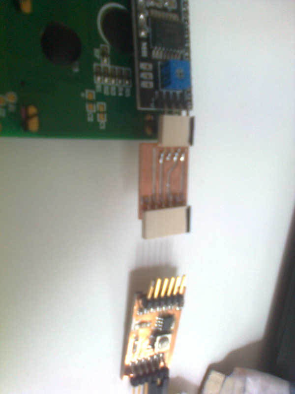
Connecting the board
After the components were soldered, I marked the ground commectors with black coloe in every connector and side of the circuit board in order to avoid problems. There were no keying used in the design, so it is possible to connect the cards in a wrong order.
Programming the device
The MCU board was connected to the computer for reprogramming.
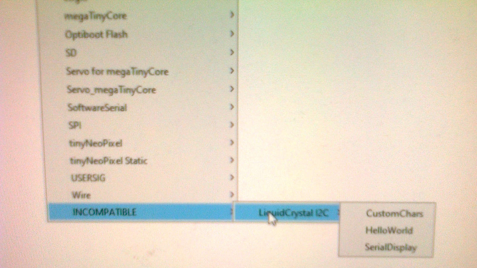
Arduino studio was opened and LiquidCrystalI2C library by Marco Schwartz was installed from Sketch -> Include Library -> Manage Libraries… . This library was required for I2C communications to the LCD display board via the LCD interface board.
Then the example file HelloWorld was loaded from * File -> Examples -> INCOMPATIBLE -> LiquidCrystalI2C -> HelloWorld*.
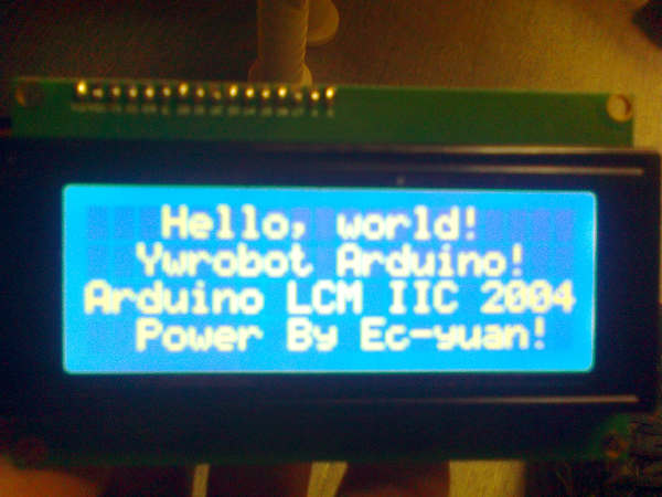
It was noted, that 0x27 is a default I2C address for the LCD and it was not changed from the default.
The unmodified example program code used for programming the device is shown here:
//YWROBOT
//Compatible with the Arduino IDE 1.0
//Library version:1.1
#include <Wire.h>
#include <LiquidCrystal_I2C.h>

LiquidCrystal_I2C lcd(0x27,20,4);  // set the LCD address to 0x27 for a 16 chars and 2 line display

void setup()
{
  lcd.init();                      // initialize the lcd
  lcd.init();
  // Print a message to the LCD.
  lcd.backlight();
  lcd.setCursor(3,0);
  lcd.print("Hello, world!");
  lcd.setCursor(2,1);
  lcd.print("Ywrobot Arduino!");
   lcd.setCursor(0,2);
  lcd.print("Arduino LCM IIC 2004");
   lcd.setCursor(2,3);
  lcd.print("Power By Ec-yuan!");
}


void loop()
{
}
The program was compliled and uploaded with the arrow, “Upload” button.
The Results
After programming the board, the adapter and the LCD board were installed to the MCU board. The board lighted up, but no text.
The board brightness was adjusted from the screw in the back of the controlled board. After the adjustment, the board worked just fine.
Modifications
First I changed the displayed text.
//YWROBOT
//Compatible with the Arduino IDE 1.0
//Library version:1.1
// This is almost a a direct copy of the example code.
// The way how the code was found is documented in the documentation
// The texts below are changed.
#include <Wire.h>
#include <LiquidCrystal_I2C.h>
LiquidCrystal_I2C lcd(0x27,20,4); // set the LCD address to 0x27 for a 16 chars and 2 line display
void setup()
{
lcd.init(); // initialize the lcd
lcd.init();
// Print a message to the LCD.
lcd.backlight();
lcd.setCursor(3,0);
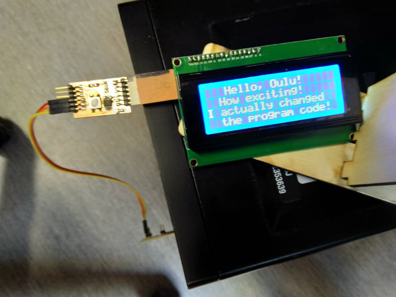
lcd.print("Hello, Oulu!");
lcd.setCursor(2,1);
lcd.print("How exciting!");
lcd.setCursor(0,2);
lcd.print("I actually changed ");
lcd.setCursor(2,3);
lcd.print("the program code!");
}
The results of the modified example code can be seen here.
Custom character feature of the LCD controller
It is possible to create programmable characters with some LCD displays. This property can be used for animation or for creating graphics. I found an example how to do it from here.
Rebuilding the setup
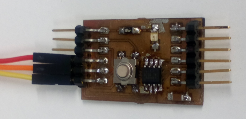
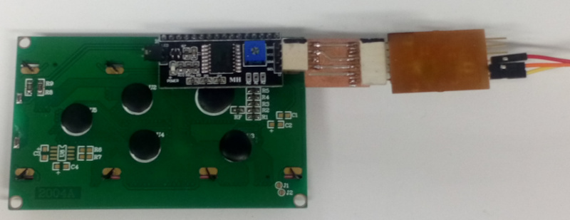
The USB programmer I used earlier was breaking. Another USB programmer was fabricated.
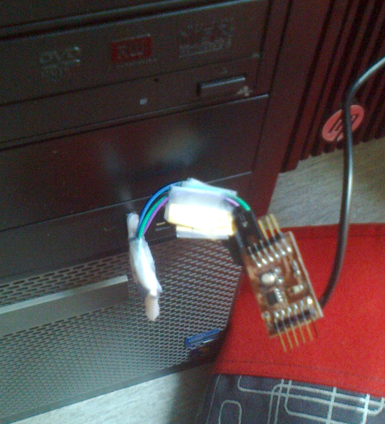
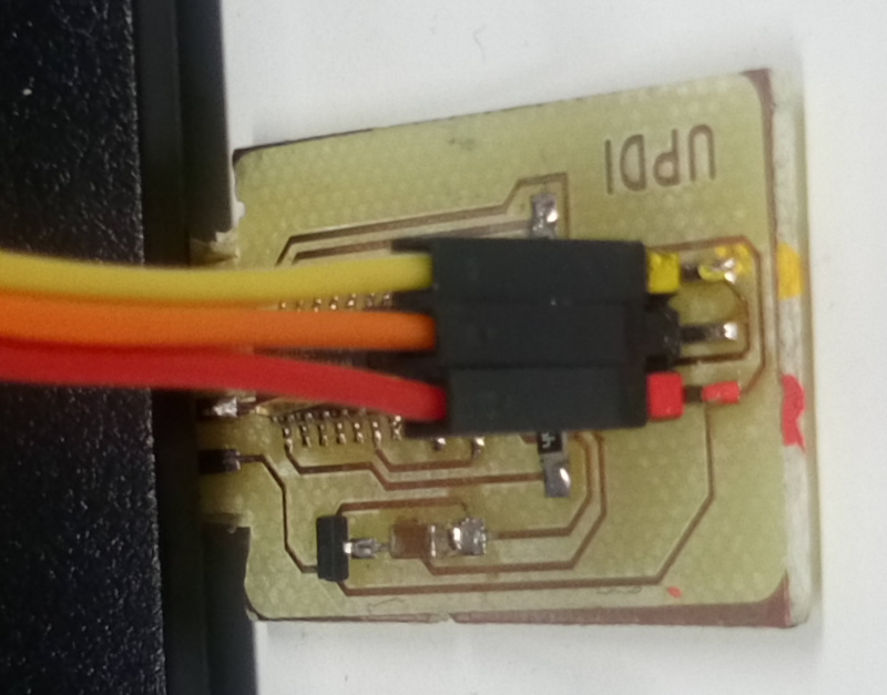
The D11C14A based USB programmer connections are shown here. Note the color coding in red and yellow in the connector on the pins matching the color coding in the wires:
The wires on the micocontroller device are shown here:
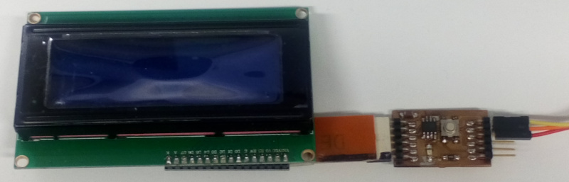
Both sides of the connected device chain are shown below. Note the black line for ground in the adapter helping in connecting the parts right.
Custom character code
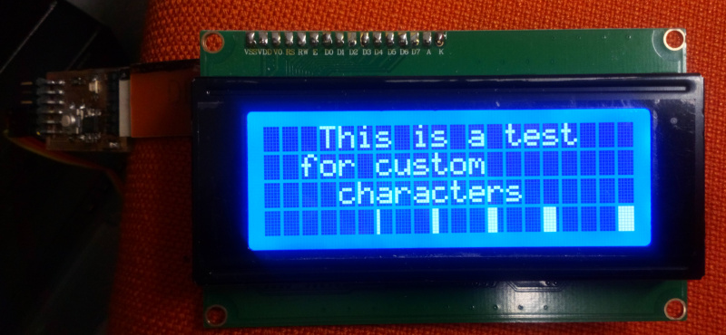
After testing that the previously programmed code still ran on the new setup connected to the host computer with the new USB controller, I made modifications to the program code so that it creates custom characters. The character arrays are defined using binary format, so it is possible to see the shape of the characters directly from the code.
The modified code containing custom character definitions is shown below:
Here is an example, how to do it.
//YWROBOT
//Compatible with the Arduino IDE 1.0
//Library version:1.1
//Modified by Antero Metso in order to try programmable characters

#include <Wire.h>
#include <LiquidCrystal_I2C.h>

LiquidCrystal_I2C lcd(0x27,20,4);  // set the LCD address to 0x27 for a 16 chars and 2 line display

// Define custom characters

byte Line1[8] = {
0b10000,
0b10000,
0b10000,
0b10000,
0b10000,
0b10000,
0b10000,
0b10000
};

byte Line2[8] = {
0b11000,
0b11000,
0b11000,
0b11000,
0b11000,
0b11000,
0b11000,
0b11000
};

byte Line3[8] = {
0b11100,
0b11100,
0b11100,
0b11100,
0b11100,
0b11100,
0b11100,
0b11100
};

byte Line4[8] = {
0b11110,
0b11110,
0b11110,
0b11110,
0b11110,
0b11110,
0b11110,
0b11110
};

byte Line5[8] = {
0b11111,
0b11111,
0b11111,
0b11111,
0b11111,
0b11111,
0b11111,
0b11111
};

void setup()
{
  lcd.init();                      // initialize the lcd
  lcd.init();

// Initiaze the custom characters

  lcd.createChar(0, Line1);
  lcd.createChar(1, Line2);
  lcd.createChar(2, Line3);
  lcd.createChar(3, Line4);
  lcd.createChar(4, Line5);

// Print a message to the LCD.
  lcd.backlight();
  lcd.setCursor(3,0);
  lcd.print("This is a test");
  lcd.setCursor(2,1);
  lcd.print("for custom");
  lcd.setCursor(4,2);
  lcd.print("characters");

   //Test the custom character 1
   lcd.setCursor(6,3);
   lcd.write(0);

   //Test the custom character 2
   lcd.setCursor(9,3);
   lcd.write(1);

   //Test the custom character 3
   lcd.setCursor(12,3);
   lcd.write(2);

   //Test the custom character 4
   lcd.setCursor(15,3);
   lcd.write(3);

   //Test the custom character 5
   lcd.setCursor(19,3);
   lcd.write(4);
}


void loop()
{
}
I would like to use this kind of graphical custom characters in my final project display.
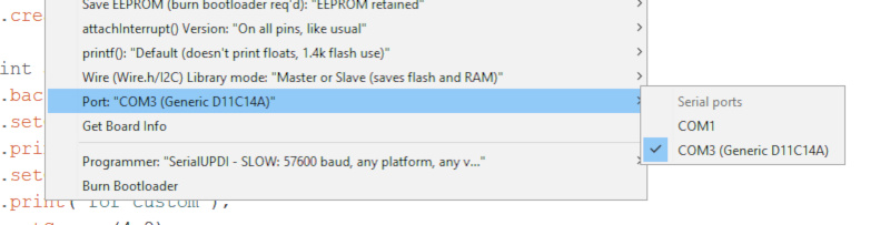
Because I re-connected the setup to the different USB port, COM port number assigned to the programmer changed. I changed the port used by Arduino IDE by Tools -> Port: … to COM3 which was available to select. The port was shown as a generic DC11C14A port. See the image below.
The custom character code was compiled in Arduino programming environment and used to program the ATtiny412 microcontroller board. The program ran and the result is shown below.
The files
Kicad files for the adapter board: