7. Electronics design
Our Homework this week:
Our assignment this week is to:
Group assignment:
- Use the test equipment in your lab to observe the operation of a microcontroller circuit board (in minimum, check operating voltage on the board with multimeter or voltmeter and use oscilloscope to check noise of operating voltage and interpret a data signal)
- Document your work to the group work page and reflect on your individual page what you learned
Individual assignment:
- Redraw one of the echo hello-world boards or something equivalent, add (at least) a button and LED (with current-limiting resistor) or equivalent input and output, check the design rules, make it, test it.

- Optionally, simulate its operation.
Learning outcomes
- Select and use software for circuit board design
- Demonstrate workflows used in circuit board design
- Abby bonus: add fun design elements (different shapes for board OR text and symbols on the board)
Have you answered these questions?
- Linked to the group assignment page
- Documented what you have learned in electronics design (in-progress)
- Explained problems and how you fixed them, if you make a board and it doesn’t work; fix the board (with jumper wires etc) until it does work.
- Included original design files (Eagle, KiCad, etc.)
- Included a ‘hero shot’ of your board
- Loaded a program and tested if your board works
This week, I designed my first custom circuit board in KiCAD!

Electronics Background
I have some electronics background, so I am not coming to this portion of the course completely from scratch. However, my training has been primarily informal. I did a bit of electronics in a mechatronics course many years ago. More recently, I began teaching a course in mixed media circuits. Given my interest in this area, one of the reasons I am excited about taking this class is so that I can improve my formal understanding of electronics as well as learn to work with surface mount components and to design and fabricate my own microcontrollers
Below are a few tutorials that are useful starting points for understanding different electronics concepts. In particular, I want to credit Nadieh Brehmer, as well as folks in the global open time for identifying these resources:
- Here is an overview of different electronic components.
- Here is some info on how electricity works.
- Here is a really useful tutorial for this week by Aalto Lab.
- Here is a really useful tutorial about integrated circuits.
Theory
- Ohm’s Law is an equation that describes the relationship between three important electrical properties: voltage, current, and resistance. Given the value of two of these properties, Ohm’s Law allows you to solve for the value of the unknown quantity. Ohm’s Law is defined as V = IR or voltage is equal to current times resistance.
A handy pneumonic device that allows you to quickly solve for voltage, current, or resistance is to draw an equilateral triangle and divide it into three sections: one on top and two underneath. In the top section, write the letter V. In the bottom left section, write I. In the remaining section, write R. Now, with your finger, cover up the letter representing the unknown quantity. If you cover up the V, you have I and R next to each other. Multiply these to get V. If you cover up the I, you have V over R or voltage divided by resistance. Cover up the R, and you have voltage divided by current.
There are many scenarios where you might want to use Ohm’s Law, but a common example would be to determine what value resistor you should use given a power supply of a particular voltage and a component rated for a particular current. This Sparkfun tutorial walks through an example of calculating what resistor to use for a particular LED.
Components
- Resistors: resistors are electronic components that slow the flow of current in a circuit. If you have ever experienced a battery suddenly getting super hot when the + and - have been connected accidentally, you have experienced a short circuit. Stick a resistor in this accidental circuit to slow that current down and keep things cool! Resistors are measured in Ohm’s. They come in all different shapes and sizes. THT resistors are marked with color bands to help you calculate their resistance, whereas surface mount resistors have values written on top.
- Capacitors
- Diodes
- LEDs
- Transistors
Integrated Circuits
The following overview paraphrases the Sparkfun tutorial on integrated circuits. Integrated circuits are at the heart of most circuits we will design. As the name suggests, an integrated circuit is a single electronic component with a tiny circuit inside made up of discrete components like transistors, resistors, and capacitors. Integrated circuits come in many different shapes and sizes and have many different functions. If you were to look inside an integrated circuit, you would see thin layers or wafers of semiconductor material, copper traces, and other materials which connect to form the electronic components that combine to create the ‘circuit’ in each IC. Together, the thin layers that are at the heart of each IC are called the ‘die’. The die is so tiny and delicate that it needs to be packaged in a housing that will allow it to be safely embedded into larger circuits.
A fun – and important! – fact is that all ICs have polarity. That is, you can’t just plug them in any which way and expect them to work. Plugging an IC in backwards is a great recipe for a smoky circuit and a dead IC. ICs therefore have markings to help you deciper the location of pin 1. Usually, this comes in the form of a small dip or notch in the center edge on one end of the package. Sometimes, there is a small circle on the left top notch of the IC. Pin 1 is always on the left top side of the IC, when a chip is held vertically with pins on the left and right and the notch is furthest from you. Occasionally, an IC is small and the markings are so tiny that it is difficult to find these normal indicators. There are also some chips that use other slight variations/cues to indicate their polarity. This site has some useful information should you want to dig deeper.
Broadly speaking, ICs and other electronic components come in two main categories: through-hole (THT or through-hole technology) and surface-mount (SMD for surface-mount device or SMT for surface-mount technology). There is tremendous variation in footrpints within the category of surface-mount devices. It is important to pay close attention when ordering SMD online if you are planning to mill and solder circuits yourself because some components will be far too small to manage by hand.
The Dual-Inline Package or DIP packege is the most common footprint you will encounter for through-hole or THT ICs. These are the familiar ICs that fit nicely into a breadboard. Pins are standardized at 0.1” apart.
If you ever spend much time searching for ICs on Digikey, Mouser, Newark or another electronics supply store, it is easy to become quickly overwhelmed. You will find many different sub-types of each IC using different, seemingly inscrutible acronyms. Some of these acronyms have to do with the shape of the packaging – i.e., the ‘footprint’ of the IC. Thanks to the Sparkfun tutorial linked above, below is an overview of the acronyms for these different footprints. Check out the tutorial for photographs!
SOIC: Small-Outline ICs are a common type of SMD that are relatively easy to solder by hand. They look very similar to the THT DIP ICs - they have the same general shape but are a bit smaller and their pins lay flat against a board rather than pokng through it. In general, when I’m looking for SMT ICs, I look for the SOIC package. The pins are usually 0.05” or 1.27 mm apart.
SSOP: Shrink small-outline packages are the same basic shape as the SOIC package but smaller. TSOP (thin small-outline package) and TSSOP (Thin shrink small-outline package) are both similar as well.
QFP: Quad Flat Packages are those square-ish chips with pins on all sides. They tend to have a ton of pins, starting at 8 per side and upwards. The pins are space anywhere from 0.4 to 1 mm apart. As per Sparkfun, variations include thin (TQFP), very thin (VQFP), and low-profile (LQFP) packages. QFN chips have the same basic square shape…but the leads are all hidden underneath! It seems these would normally be soldered with a reflow over rather than by hand.
The last package they mention on the Sparkfun site is a Ball Grid Array (BGA) which, like the QFN chips, have all connections underneath rather than splayed out to the side. However, these chips seem to have more connections than the QFN chips which are in unusual configurations. I’m glad that thus far, I’ve not been called on to solder a QFN or BGA component! 
Common types of ICs
There are a huge variety of integrated circuits. The Sparkfun tutorial mentions a few that you might come across regularly: logic gates, microcontrollers, as well as sensors like temperature sensors, accelerometers, gyroscopes, and more. While these sensors are technically ICs, they are usually smaller than the microcontrollers and logic gates that we typically think of when we talk about ICs. These logic blocks look like a really fun and intuitive teaching tool to help introduce folks to logic gates.
Now that we have explored common types of ICs, time to dig into the specific IC at hand, the ATTiny412.
Reading the Datasheet


Technically, reading the datasheet is assigned during the embedded programming week. However, it never hurts to take a look at this info to better understand the components we are using!
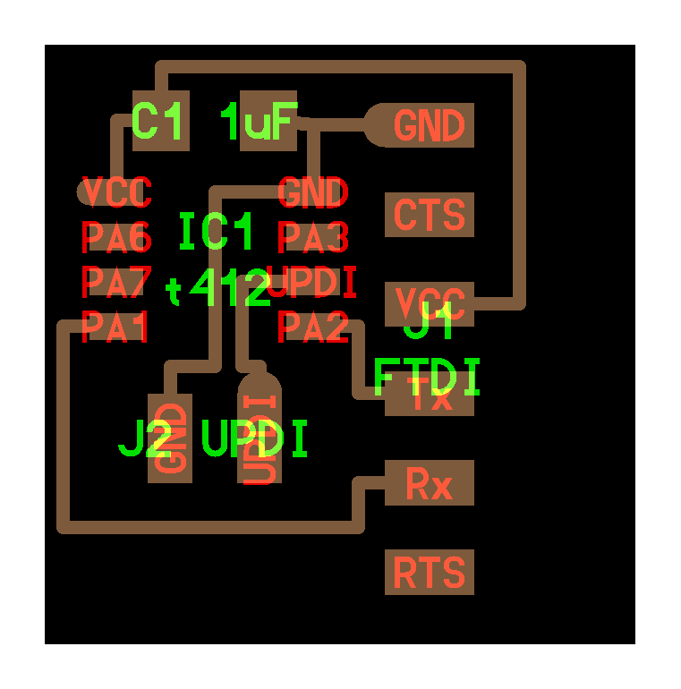
The datasheet for the AT Tiny 412 is here. I decided to use the AT Tiny 412 because there is a detailed tutorial for it thanks to the Aalto lab, because we have the microchip at LCCC, and because my instructor suggested it was a simple place to start. As the data sheet points out, the 412 has eight pins and 4 KB of memory. Compared to some of the other chips in this family, it seems like the biggest distinction is in the number of ADC channels and the number of general purpose inputs and outputs. It is useful to note that many of the pins on the micro controller can be programmed. Even some of the pins that have default uses, like the TX and RX pens, can be overridden in software.
I began by reading through the table of contents, which itself is pretty extensive. In the past, when I have reviewed datasheets, I focus only the pinouts. So, I wanted to see what else I could take away from the information provided. The vast majority of the content of the datasheet is listed under the ‘Features’ subheading. After a section devoted to clarifying the datasheet itself, the first several sections provide broad brushstrokes about the microcontroller, including a block diagram, pinout information, and details about the device memory, architecture, and CPU. Sections 9 - 13 explore different device controllers. Of the subsequent headings, 15 and 16 are about ports (port multuplexer and I/O, respectively); of the remaining subheadings, VREF, RTC, USART, Serial Peripheral Interface, ADC, DAC, and UPDI all stood out to me as sections that might provide useful / interesting information.
This datasheet describes several microcontrollers, including the ATTiny 412, 212, 414, 214, and 416. A table compares the number of pins, amount of RAM, flash memory, ROM, the maximum frequency, and the timer/counter types available, among several other features. There is a lot of similarity across devices, where they differ most is in the number of ADC channels available, the general purpose I/O, and the external interrupts. This makes sense because each of these categories would be tied to an external input, and the biggest difference between these chips therefore seems to be in the number of pins across different devices.
The block diagram is a bit opaque to me. While I recognize some of the acronyms and can follow the helpful color-coded chart, it is difficult to understand the relationship between the different blocks in the abstract, nevermind how it all relates back to the physical hardware of the chip.
The pin-out diagram is more straightforward: most pins (all except VCC and ground) can be programmed to serve in different capacities. Some pins have special functions (UPDI for programming/debugging the chip and the clock/crystal pin). This format holds true for both the 8, and 14 pin SOICs. The 20 pin SOIC and 20 pin VQFN are mostly the same, however they each have several dedicated digital pins in addition to the pins with multiple functions.
I was getting a bit lost in the datasheet’s discussion about multiplexing so I decided to dig a bit deeper. I particularly like this multiplexing tutorial which helped clarify how several inputs, for example, could be routed to a single output, using bits to assign/direct which channel is sent, as illustrated in the ‘multiplexer input line selection’. This didn’t fully illuminate / clarify the datasheet for me, but it did help to begin to unravel it a bit further.
There is quite a bit more to unpack in the datasheet, but in the interest of time I will skip over the rest of this for now. However, I want to highlight a few additional acronyms that get tossed around quite a bit…
FTDI, UPDI, TX, RX
It is easy to get overwhelmed trying to keep track of all the different letter combinations and their meanings.
UPDI - UPDI stands for Universal Programming and Debugging Interface. It is a 2-pin connection/communicaton protocol that you use to program your microcontroller. One of the pins in this two-pin connection is UPDI, the other is ground. The UPDI pin can both transmit and receive data. You can add a third pin for power or else power your board from a separate FTDI connection. While I used the 2-pin connector this time around, it seems like it would be wise to build the 3-pin UPDI to FTDI converter board so that I don’t have to plug in a second FTDI cable just for power on future boards.
FTDI & UART - The best explanation I found online about UART and FTDI is here. FTDI stands for Future Technology Devices International, a semi conductor company. UART stands for Universal Asynchronous Receiver-Transmitter. Arduinos and other microcontrollers are UART devices that transmit and receive serial data. An FTDI cable connects a UART device to a computer via USB. An FTDI cable has separate pins assigned to a microcontroller’s TX and RX pins.
TX - The TX pin on a microcontroller transmits data to another device.
RX - The RX pin on a microcontroller receives data from another device.
Learning KiCAD

KiCAD Resources
Here is the board I am starting with. You can find the board layout and the components for this board here.
Below, in particular, I am following step-by-step through the Aalto lab kiCAD tutorial by Kris which you can find here.
The KiCAD Workspace


Getting KiCAD Set up
Before you begin designing your PCB, you will need both symbol and footprint libraries for the components you will be using in your design. You can acquire these libraries in several different ways. You can use some of the default libraries that come with KiCAD, you can go to DigiKey (or wherever you purchase your components) and install their libraries, you can download footprints and symbols from sites like SnapEDA. Or, you can make your own libraries with custom parts. (Digikey has a great set of KiCAD tutorials that cover both footprint and symbol design. Note that they are using a slightly older version of the software so not every instruction will line up perfectly with your GUI, but check the comments for helpful hints.) Thanks to Kris from Aalto Lab, we have a custom set of components in a Fab library that we can use to help speed up our design process.

Footprints Library
You can find the Fab Academy KiCAD library here. To install the library, begin by downloading the zip file. Unzip the file, and put it somewhere where you will be able to find it subsequently. You might want to rename the file to fab. KiCAD does not care where you put the file as long as you tell the library manager where to find the library file.
After you download the library, you need to add the Fab pretty folder within the footprint libraries in order to access it in your project. You can choose to access it locally, for the current project only, or globally, for all projects. Though I originally installed the libraries before Fab Academy started, I decided it was worth installing again to make sure I had the most up to date version.
To see the 3D renderings, and you need to configure pants. Kris demonstrates defining a variable called Fab and pointing it to the fab library.
Symbol Library
To import the Fab symbol library, go to preferences, and select “manage symbol libraries”. If you are going to only use the Fab Academy library, as Kris describes, you can uncheck the default libraries that kiCAD installs and leave only the Fab library checked. You will also need to specify the location of the library and the file path.


Making Your Schematic
Open your schematic editor, and either click on the symbol for adding a component to the right, or click ‘A’ to pull the component dialog. Now you need to search for the component you would like to add. I searched for Fab 412 and found the IC that I needed. After you place the part, you can right click to explore the properties of the part. For example, you can see that this part already has a footprint associated with it.
Now it is time to begin the process of building the schematic. The hot key for moving a component in the schematic diagram is M. The hot key for adding wires is W. You can follow the connections on the board that is provided in order to begin drawing your schematic.
You can use labels to connect parts of the schematic that you don’t want to have to connect with wires. You just need to hover over the relevant connection point and click L, label what you want to call the connection, and then do the same at the location where you want to make the connection. Be sure the names at the two connection points match precisely!
For items that are not connected to anything else in the schematic, you should use the little X icon to indicate no connection. If you do not add the ‘x,’ KiCAD will throw an error when you do an electrical rules check: it will indicate that not all connections have been made.
Next, we need to connect the RX and TX pants for serial communication. Here, you need to check the data sheet to understand which pens are set to TX and RX by default. Pins PA6 and PA 7RTX and RX respectively. I noticed that the new symbol has RX, TX, and UPDI clearly labeled. The only thing that is a little bit confusing is that PA six and PA seven are not labeled as six and seven in the connection points. The relationship between the physical pins, their internal labeling mechanism, and their connection to the Arduino pin values can be somewhat confusing.
To connect the UPDI terminal, we use the label feature to connect UPDI to pin 6 and GND to the common ground.
Next we are connecting the button and LED. To do this, begin by rotating the resistor and moving the button and LED to a better location. Next, use labels to assign connection points for the LED and button, and connect both the button and LED to ground through a junction.
Use the “annotate sketch” button to number the components on your sketch. Initially, the part numbers will just have a question mark. The “annotate sketch” button adds numbers automatically. After you annotate your sketch, you can use the debug feature, which allows you to check whether there are any electrical issues in your design. In KiCAD 5, the debug button is a little ladybug.
Here, you can see that there are two error messages. As Kris describes, these error messages are due to the fact that KiCAD expects information about the sources of the power and ground. Add power flags using the power port button to resolve this error.
After you have created your schematic you should check the foot prints to make sure that they are associated with the symbols in the schematic before your generate your NET list.
PCB Editor


After you generate your NET list, you can open the PCB editor. You will have to import the NET list to see your components in this layout. If you need to make changes to your schematic, you can do so back in the schematic editor, but you will always need to update your NET list. In later versions of KiCAD, this process is replaced with the ‘update board from schematic’ feature.
When you import your NET list to the PCB editor, you will see the components randomly grouped on the page with thin white lines connecting components as designated in the schematic. This initial state with the tangle of thin white lines is called a ‘rat’s nest’. From this rat’s nest, your task is to lay out the components on the board in a manner that limits collisions of the white lines. You also need to pay attention to the placement of certain components like terminal connectors, antenae, coupling capacitors, and so on, because the physical location of these elements can impact their functionality.


Before you begin routing your traces, you need to double check design rules to ensure that the design you create will work for your mill. So, for example, you need to check the mininum track width, the minimum clearance, and the size of the vias, where relevant. (A via is only relevant if you are working on a two-sided PCB or are using thru-hole technology.) You can adjust these elements in preferences, but you can also find this menu in the upper lefthand corner of the PCB layout window. For the end mills we are using for Fab Academy, you should set your minimum track width and clearance to 0.4 mm. Thus far in my designs, I am always using the minimum track width and clearance. There are occasions when larger tracks are preferred, however that is beyond the scope of this first design assignment. Sometimes it takes a few tries to find a good board layout and to route the tracks in a sensible manner. I definitely had to try a couple of times before I was happy with my design.
Thanks to Kris’ tutorial, I chose to use a copper pour to connect ground. There is some controversy, it seems, about whether this is best practice. However, when milling, there will always be some amount of copper pour by default (you have to put in extra effort to avoid this). So, you might as well make sure that your copper pour is grounded. To design a PCB with a grounded copper pour, you first route all traces except for ground. Then, you create your board layout by drawing an outline of the board using the graphic lines tool on the drawing layer. You may want to adjust the grid setting, for example to 0.5 mm, so that it is easier to understand the size of your board in terms of mm.
Next, it is time to place the copper pour. Navigate to the front copper layer or FCU. Then select the “add fill zones” layer and left click to pull up the dialog box where you will select “ground”. Left click on the path of the polygon you want to draw. If you try to ‘escape’ and start a new polygon, none of the fill zone settings you have created will hold.
After you create your copper pour, you are almost finished! However, for your mill to interpret the proper initial XY position of your board when you go to mill your design, you need to create a margin. Use the graphic lines tool in the margin layer to create a margin 2 mm around your board. When you import your design into modsproject to generate the G Code, it will ensure that the XY position of your board is offset by the distance of the margin to the board outline. You should next use the drawing layer and the polygon tool to trace and cover the actual area of the board. When you export files from KiCAD, this will be a separate layer that you will import into mods to generate the G-Code for cutting the board itself out. Select the polygon layer you just added and hit “e” to edit the dimensions. Edit the line thickness to zero.
MODS Project
For this assignment, I used Neil’s version of mods because in global open time some of the instructors said that the community edition sometimes has issues with the SVG files generated by KiCAD but that Neil’s version works fine. The process is very similar to what I outlined in the Electronics Production homework, so I will not review it in detail here. However, below you can see screenshots of the process


Troubleshooting
Below are a couple of items that came up for me early in my learning process with KiCAD:
- When I first started working in the schematic editor in KiCAD, I ran into an incredibly confounding issue where I could not connect any components with wires at all. I would watch a tutorial and they would be clicking away with no problem, connecting different components in their schematic, and I could not get a single component connected to anything else! I did some googling and it turned out that it was an issue with the size of my grid. I checked the library editor and discovered that the symbols were created on a 1.27 grade and the grid in KiCAD was defaulting to 1 mm. I tried just changing the grid and attempting to connect items that I had already placed, but I discovered that in the end, I needed to actually first change the grid to 1.27 and then import of the symbols again so that they would allow for connections with wires.
- Occasionally, I wanted to end a wire without actually connecting it to anything (for example, because I was going to subsequently add a label to the wire to make the connection). I didn’t know how to do this at first, but all you need to do is to double click to end a wire that is not at a normal connection point.
- When I went to open the footprint dialog in order to check on the footprints that should have automatically been assigned it appeared the KiCAD was having trouble identifying the location of the foot prints. It said that there were no footprints with the nickname fab. As it turned out, I had named the footprint library fab pretty foot, and it needed to simply be named fab. When I change the name and open the footprint editor, I was able to right click and view footprint just fine. -If you need to selectively edit a copper pour area, use a no-fill zone and then use the ‘b’ key shortcut to recalculate the pour.
- At one point, my computer shutdown unexpectedly. When I restarted the machine, KiCAD seemed to think it was already running when it was not. I ran into issues where I could not open a PCB file because it thought it was already open. This had to do with the file being locked. I found this command on a forum to run in terminal:
rm ~/Library/Caches/kicad/*.lock
After I ran this, when I opened KiCAD and clicked on the schematic or PCB editors, they would not open until I also clicked on the symbol and footprint editor. After I did that, I closed the symbol and footprint editors and was able to continue as before.
Global open time


Symbol libraries


Footprint library


File organization


Adding symbols to the library


Milling
Milling my board went relatively smoothly. In terms of design, the main thing that I had to make sure to do was to adjust the minimum trace size as well as the minimum space between traces. I followed the Aalto lab online tutorial to adjust these values. To adjust the design rules, you have to go to file board set up and then when the dialogue opens you have to choose design rules. Based on the tutorial, I said the track and clearance birth 0.4 mm. Track is the minimum width of the traces and clearance is the minimum distance between traces.

After the KiCAD file was set up and ready to go, I opened UGS, the Universal GCode Platform software I use to control my desktop mill from my computer.


For a more detailed overview of the milling process, please review my electronics production week post.


While the milling went smoothly, I did run into one strange issue with my GCode file. The mill began by raising the Z axis very quickly and then pausing in place for a long period of time. I searched for some information about reading GCode and discovered that the issue is the section of GCode below where it seems to say to rapidly move the z-axis, turn on the spindle, and then pause for 1000 seconds.
G00Z2.0000
M03
G04 P1000
G00Z2.0000
I deleted the following section:
G04 P1000
G00Z2.0000
After that fix, it seems like it is working correctly. However, I also lost a board because I forgot to take this same bit of GCode out of the file that I made to cut the perimeter of my board. I had to hit the e-stop to get it to stop and lost my zero settings. I tried to approximate the zero settings to cut the board but didn’t account for the offset at the beginning and ruined my first board. Luckily, I was able to cut a second board more easily! I am very glad I ran the air test to figure this all out.


## Soldering
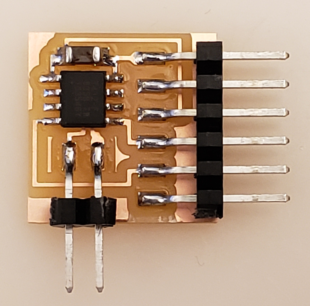
When I went to solder the board I realized that this was not going to be quite as straightforward as the previous iteration. This is because with the previous board, we were provided with a precise detailed list of the components, as well as information about the orientation of the microcontroller.


In the electronics production assignment, here were no other polarized components. With the board that I designed, I have two LEDs which are polarized. I initially was worried that I wasn’t going to be able to figure out how to orient my LEDs. I had forgotten that I had taken photos of the bags the LEDs were in in order to ensure that I had the component information so that I could look up the data sheet. At first, when I looked at the LEDs I did not notice any visual cue to indicate which side was anode or cathode. Looking at other students documentation, I saw that there was some visual information on the back of the LED. But when I looked at the back of the LEDs that I had on hand I didn’t see any lines as indicated in the other students documentation. However when I looked up the data sheet, I noticed that there is a green line on one side to indicate the cathode side of the LED, and that was enough information to help me understand how to orient the LED on the board. Cathode goes through the resistor to ground.

I realized I needed to double check that the resistor values I had borrowed from the lab were going to be correct. I looked at the data sheet for the LED. Knowing that the FTDI cable was going to be supplying 5 V to the circuit, and knowing that the LEDs voltage is 1.8 V, and 20 mA, I used this LED resistor calculator that I found on Nadieh’s site to discover that the resistor that I needed was 200 Ohms approximately. When I was in the lab earlier in the week, I had grabbed some 1K, 5K, and 10k resistors. My instructor agreed that the 1K resistor should be fine for this purpose, since in many contexts resistance can be somewhat flexible.
I also received some extra help from my instructor with soldering the button to the board, since this component was more difficult than the others. When he inspected my board with a microscope (and when I checked with the microsope myself, subsequently), we found a few areas that were not adequately soldered, so he helped touch up these areas a bit.
Programming Electronics w/MegaTinyCore and SAMD11c
Below is an overview of how to use the Arduino IDE and a homemade SAMD11c programmer board to program a DIY custom microcontroller. My instructor sent me a link with documentation about how to use the MegaTinyCore on Arduino in order to program the board.
Here is a GitHub repository with information about and resources for megatinycore, which provides Arduino support for all tinyAVR chips. If you want to program your custom board using the Arduino IDE, this site provides a lot of background information as well as the board manager and installation instructions you should use to get started.
The first step in this process is to add the relevant board manager to your IDE. You can do so under preferences
He said to start by taking a particular url and including it in the preferences section under the heading of other board manager URLs. I also had to go to tools drop-down menu where I selected boards and then board manager, and this is where I was able to install the relevant details for the AT Tiny Mega Core. From here after the installation was complete I just had to select the correct serial port the correct board. Initially, I missed the step where I needed to change the programming communication protocol to UPDI slow. As a result I received a Java error. After changing that programmer information, the board programmed , and we were able to upload a blink sketch very easily.
MegaTinyCore
Installing this: https://github.com/SpenceKonde/megaTinyCore https://github.com/SpenceKonde/megaTinyCore/blob/master/Installation.md
Put this in the additional board manager URL: http://drazzy.com/package_drazzy.com_index.json Having soldered my board, it was now time to set it up. We connected the Sam D11C FTDI board that I made last week to the UDPI adapter and through the UDPI adapter to the new AT412 board. We then hooked up an FTDI cable to provide power to the board.


Using Homemade Programmer Board to Program the LED on my DIY Board to Blink
During the electronics production week, I got as far as milling and soldering two programmer boards and installing a new board manager to get my Arduino IDE set up to talk to the SAMD11C programmer. Please visit the “Installing Arduino Core board manager” section of my electronics production assignment for more details on this process.
Last week, however, I did not have the opportunity to test that my programmer was actually functional. For this week’s assignment, with the help of my instructor, I was able to use my homemade progammers to program my DIY microcontroller!
Arduino


