Electronics design
Design a development board to interact and communicate with an embedded
microcontroller.
Group assignment:
Group assignment
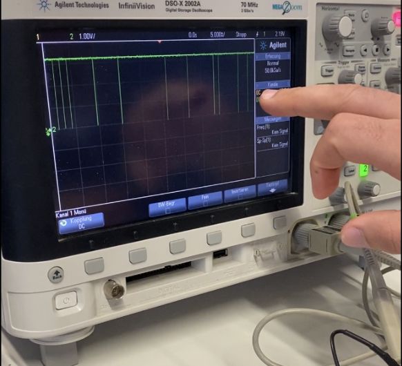
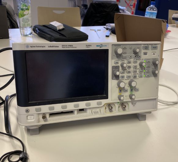 The oscilloscope.
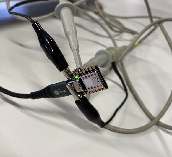 Connecting the oscilloscope to the 5V and 3V3 power pins of the
SAMD21.
Connecting the oscilloscope to the 5V and 3V3 power pins of the
SAMD21.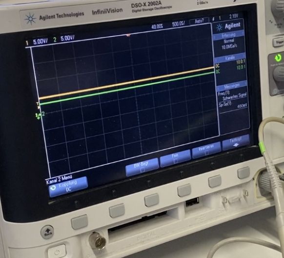 The oscilloscope measures the voltage very accurately: 5V
(yellow) and 3V3 (green).
The oscilloscope measures the voltage very accurately: 5V
(yellow) and 3V3 (green).This version of the sketch is truly the simple blink sketch. It uses digitalWrite to write HIGH for 1 second and then LOW for 1 second to a pin:
// the setup function runs once when you press reset or power the board
void setup() {
	// initialize digital pin LED_BUILTIN as an output.
	pinMode(7, OUTPUT);
}

// the loop function runs over and over again forever
void loop() {
	digitalWrite(7, HIGH);   // turn the LED on (HIGH is the voltage level)
	delay(1000);                       // wait for a second
	digitalWrite(7, LOW);    // turn the LED off by making the voltage LOW
	delay(1000);                       // wait for a second
}
This sketch is slightly modified: It uses analogWrite to write an analog signal (number
between 0-255) to a pin:
// the setup function runs once when you press reset or power the board
void setup() {
	// initialize digital pin LED_BUILTIN as an output.
	pinMode(7, OUTPUT);
}

// the loop function runs over and over again forever
void loop() {
	analogWrite(7, 128);   // 128 is the pwm signal
}
Here, we're connecting the oscilloscope to pin number 7 (as
described in the sketch above) and to GND. You can see, that the oscilloscope measures
the HIGH and LOW very accurately. Jumping from 0V to 3V3 every second as described in
the code.
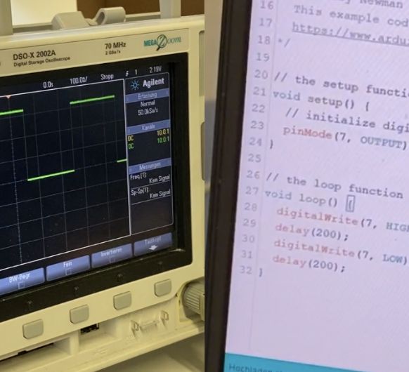 Here, we changed the delay in the code to 200ms. The
oscilloscope picks it up (grid is 100ms).
Here, we changed the delay in the code to 200ms. The
oscilloscope picks it up (grid is 100ms).
Trying to measure the same thing with the multimeter is very
inaccurate.
 Now we're using the analogWrite code set to 255. Using an analog
signal, some disturbances can be seen (short moments in which the power is down)
Now we're using the analogWrite code set to 255. Using an analog
signal, some disturbances can be seen (short moments in which the power is down)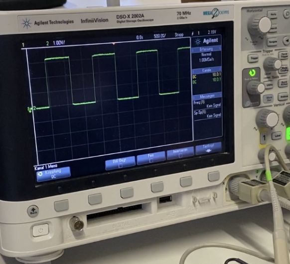 We're now setting the analogWrite to 128, so exactly half. With
the oscilloscope, it's visible that the signal is exactly half of the time HIGH and half
of the time LOW, as it should be.
We're now setting the analogWrite to 128, so exactly half. With
the oscilloscope, it's visible that the signal is exactly half of the time HIGH and half
of the time LOW, as it should be.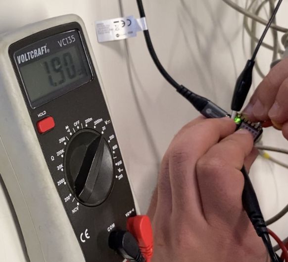 Now
testing the same thing with the multimeter: It only picks up
the average, which is about 1.9V
Now
testing the same thing with the multimeter: It only picks up
the average, which is about 1.9VBoard Features
I'm designing this PCB to work with my XIAO Seeduino SAMD21. To see its' features, go to my Embedded programming assignment. This SAMD21 can be programmed via USB and doesn't need pins for that. The following I/O-devices will have to connect to the board, since I want to use it for my final project:
- 2x HC-SR04 ultrasonic distance sensor
- 1x peristaltic pump
Also needed:
- 1x MOSFET to drive the pump
- 1x button to test its' functionality
- 1x 5V regulator
- Resistors, Capacitors, LEDs etc
The board also includes a programmable button and an LED that turn on on receiving power (plus the needed capacitors and resistors).
Designing the PCB in KiCad
Library preparation:
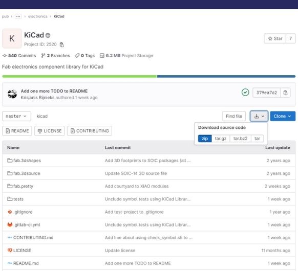 Go
to
this link
to download the FabAcademy KiCad libraries. Download as ZIP.
Go
to
this link
to download the FabAcademy KiCad libraries. Download as ZIP.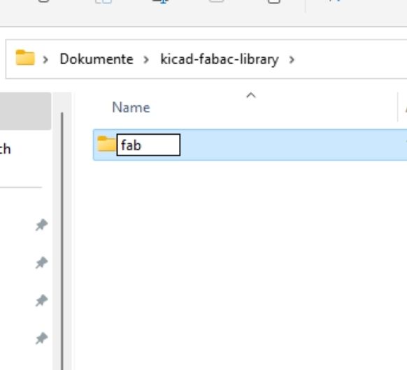 Extract and
rename to "fab".
Extract and
rename to "fab".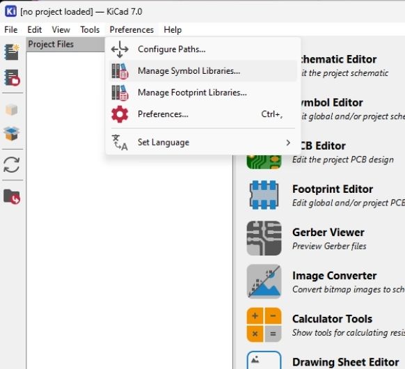 Without any
project loaded, go to Preferences>Manage Symbol Libraries
Without any
project loaded, go to Preferences>Manage Symbol Libraries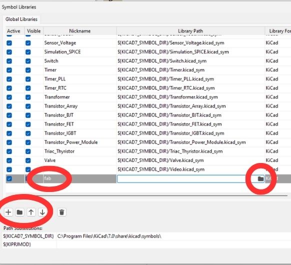 Here, click the
Plus and name it "fab". Then click the folder.
Here, click the
Plus and name it "fab". Then click the folder.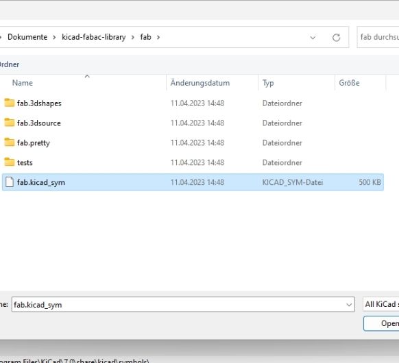 Add
this file.
Then close the window by pressing OK. Symbol Library is now added!
Add
this file.
Then close the window by pressing OK. Symbol Library is now added!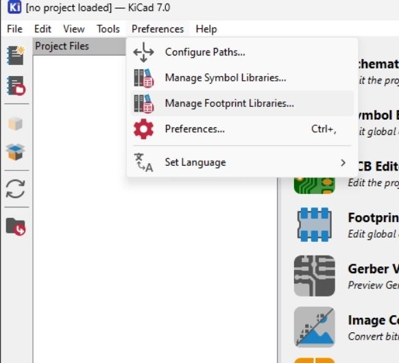 Go
to Preferences>Manage Footprint Libraries.
Go
to Preferences>Manage Footprint Libraries.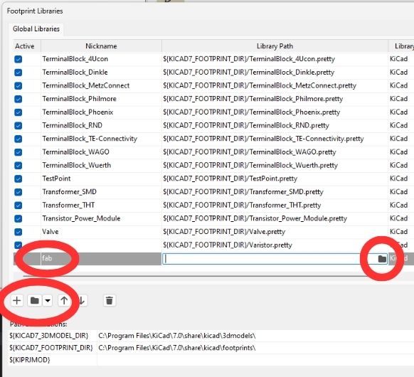 Here, click
the
Plus and name it "fab". Then click the folder.
Here, click
the
Plus and name it "fab". Then click the folder.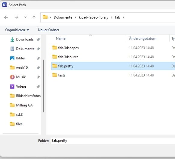 Add
this
file.
Then close the window by pressing OK. Footprint Library is now added!
Add
this
file.
Then close the window by pressing OK. Footprint Library is now added!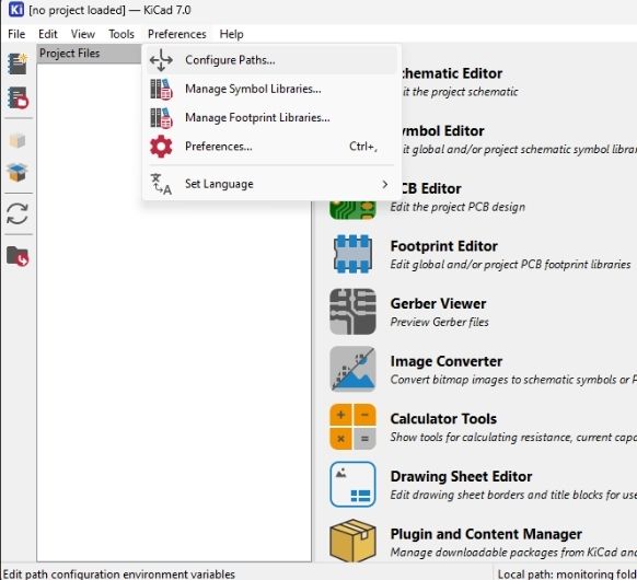 Now
go to
Preferences>Configure Paths
Now
go to
Preferences>Configure Paths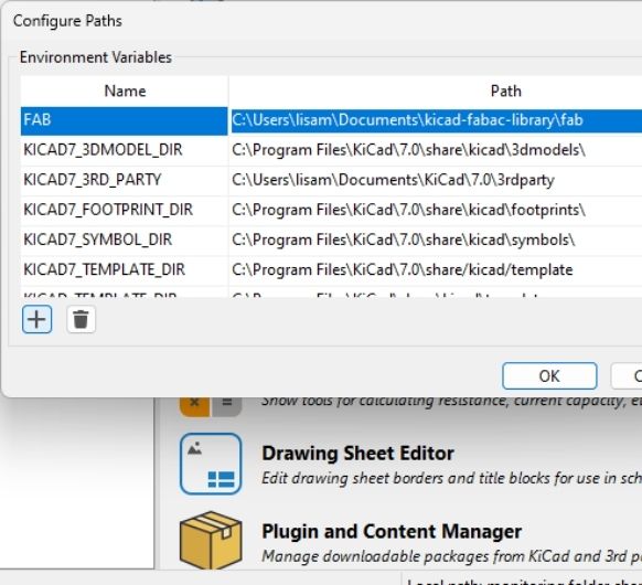 Create new,
name it "FAB" and add the "fab" folder. Now you are set to use the Fab Libraries.
Create new,
name it "FAB" and add the "fab" folder. Now you are set to use the Fab Libraries.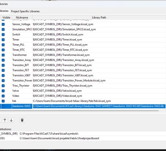 You also
need to include the SAMD21 symbol and footprint. To do so, go to https://wiki.seeedstudio.com/Seeeduino-XIAO/#resourses
and download the KiCad file. Repeat the process from above for this file as well. In
Symbol libraries, add the "SeeduinoXIAO.lib".
You also
need to include the SAMD21 symbol and footprint. To do so, go to https://wiki.seeedstudio.com/Seeeduino-XIAO/#resourses
and download the KiCad file. Repeat the process from above for this file as well. In
Symbol libraries, add the "SeeduinoXIAO.lib".
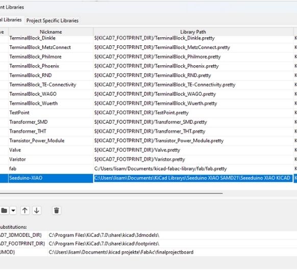 In
footprint
libraries, add the folder which contains this .lib file.
In
footprint
libraries, add the folder which contains this .lib file.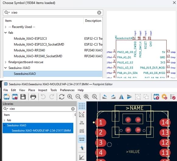 You should
now
have both the symbol and the footprint.
You should
now
have both the symbol and the footprint.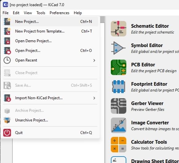 File>New Project to create a new project.
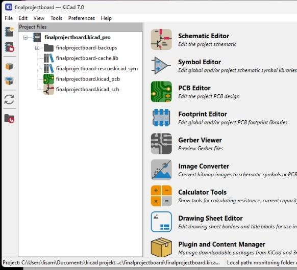 My
project
My
project Double click the
schema file.
Double click the
schema file.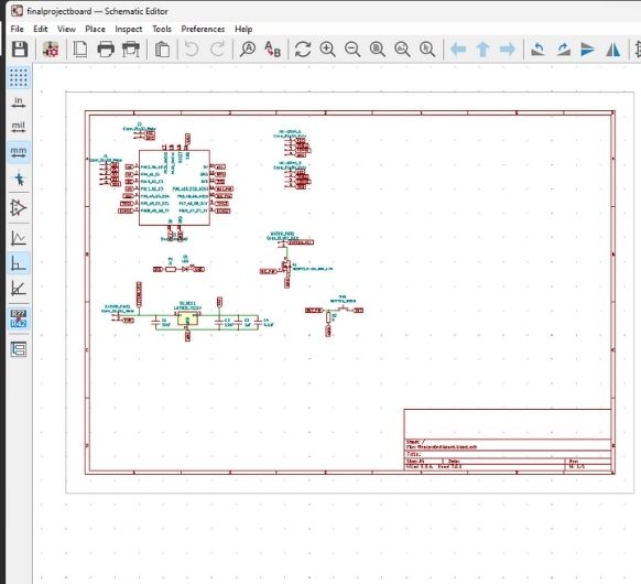 This should
open, in your case everything will be empty of course if you haven't added anything yet.
This should
open, in your case everything will be empty of course if you haven't added anything yet.
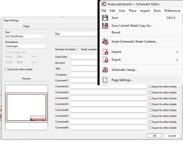 By
going to
File>Page settings you can change the size of the sheet and the metadata. I never really
use it, but do whatever you prefer!
By
going to
File>Page settings you can change the size of the sheet and the metadata. I never really
use it, but do whatever you prefer!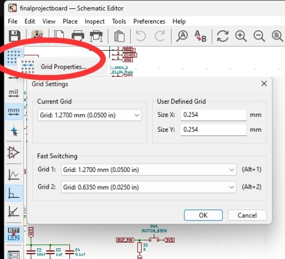 An
important
thing to note though is the Grid and its' properties. If you want to change the Grid,
right click on this button and click Grid properties.
An
important
thing to note though is the Grid and its' properties. If you want to change the Grid,
right click on this button and click Grid properties.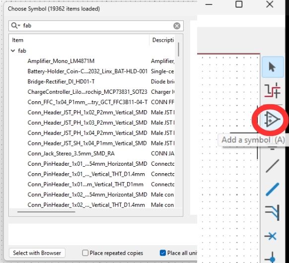 Now to the
important functionality: With this button, you can add symbols. The window on the left
will open, where you can find all symbols KiCad has to offer, also the ones you just
added. You can use the search function to quickly find what you need
Now to the
important functionality: With this button, you can add symbols. The window on the left
will open, where you can find all symbols KiCad has to offer, also the ones you just
added. You can use the search function to quickly find what you need 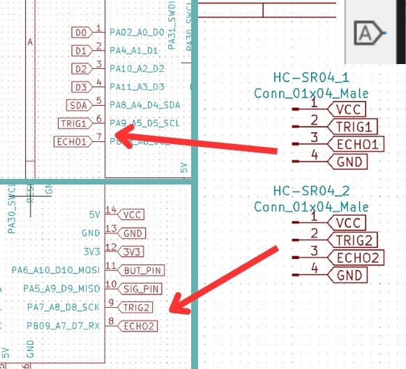 Added 2 pin
headers for both HC-SR04's. I create the connection logic with labels. This way, I can
connect two pins without drawing a cable.
Added 2 pin
headers for both HC-SR04's. I create the connection logic with labels. This way, I can
connect two pins without drawing a cable.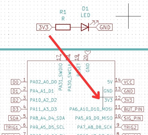 The LED: by
connecting it to 3V3 it automatically turn on, when power is supplied to the board.
The LED: by
connecting it to 3V3 it automatically turn on, when power is supplied to the board.
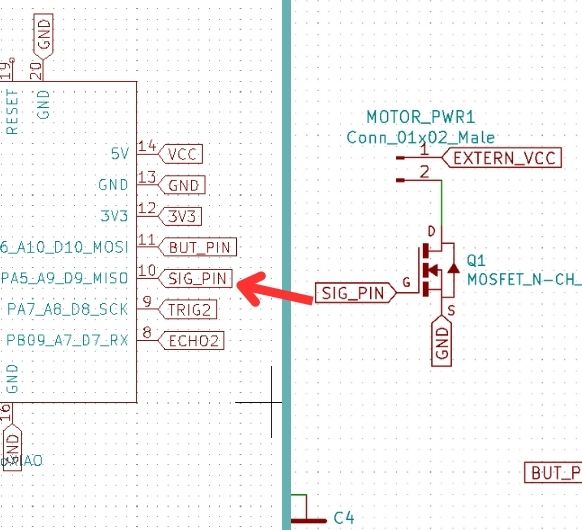 The pump: A pin
header serves as the connection place for the pump. A MOSFET is integrated into this
circuit
to control the pump. Gate pin is connected to the SAMD21, when power is supplied to this
pin, the circuit of the pump gets closed and it can work -> SIG_PIN can be programmed.
Pump
get power from 12V adapter, so it's not connected to normal VCC, but to EXTERN_VCC.
The pump: A pin
header serves as the connection place for the pump. A MOSFET is integrated into this
circuit
to control the pump. Gate pin is connected to the SAMD21, when power is supplied to this
pin, the circuit of the pump gets closed and it can work -> SIG_PIN can be programmed.
Pump
get power from 12V adapter, so it's not connected to normal VCC, but to EXTERN_VCC.
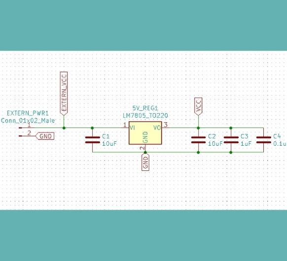 5V
regulator: On
the left, we have the pin header which serves as the place to connect the 12 power
adapter.
The 5V regulator in the middle turns 12V into 5V and "connects" EXTERN_VCC and normal
VCC.
Capacitors between the 5V regulator and the GND are neccessary.
5V
regulator: On
the left, we have the pin header which serves as the place to connect the 12 power
adapter.
The 5V regulator in the middle turns 12V into 5V and "connects" EXTERN_VCC and normal
VCC.
Capacitors between the 5V regulator and the GND are neccessary.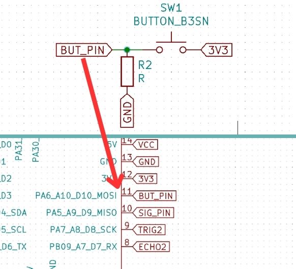 The programmable
button with a pull-down resistor: In a circuit, a "pull-up" or "pull-down" resistor is
used
to ensure that a digital input signal is in a well-defined state when no input is
present.
This
pull-down resistor connects the input to ground, so that when the button
is not pressed, the input is at a logic low level. When the button is pressed, the input
is
connected to the voltage source through the button, and the input goes to a logic high
level.
The programmable
button with a pull-down resistor: In a circuit, a "pull-up" or "pull-down" resistor is
used
to ensure that a digital input signal is in a well-defined state when no input is
present.
This
pull-down resistor connects the input to ground, so that when the button
is not pressed, the input is at a logic low level. When the button is pressed, the input
is
connected to the voltage source through the button, and the input goes to a logic high
level.
What to do after you added all of your components: From logic to layout
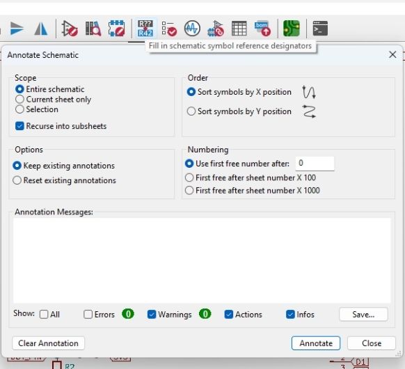 First,
annotate all symbols with this button. As it already says,
it fills in all of the missing symbol reference designators.
First,
annotate all symbols with this button. As it already says,
it fills in all of the missing symbol reference designators.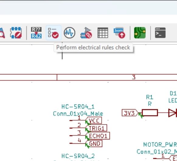 You also
might want to run an ERC to check if you violate against
any important electrical rules in you design that might harm you pcb.
You also
might want to run an ERC to check if you violate against
any important electrical rules in you design that might harm you pcb. 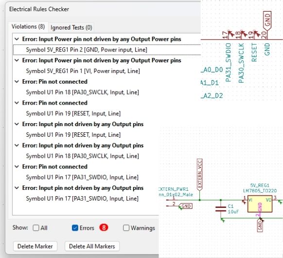 I get a
few errors, but I know why they are there and why they
aren't a problem. They refer mostly to these 3 pins that aren't connected, which isn't a
problem, because they aren't regular I/O pins, but they are below the board and aren't
important for the main circuit. The other errors come from the 5V regulator, because the
program doesn't know that EXTERN_VCC refers to a power input.
I get a
few errors, but I know why they are there and why they
aren't a problem. They refer mostly to these 3 pins that aren't connected, which isn't a
problem, because they aren't regular I/O pins, but they are below the board and aren't
important for the main circuit. The other errors come from the 5V regulator, because the
program doesn't know that EXTERN_VCC refers to a power input.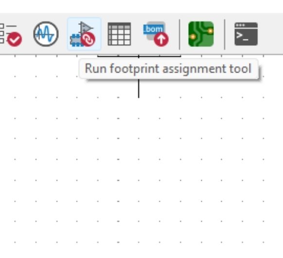 Time to
assign the footprints to the symbols. Run this tool.
Time to
assign the footprints to the symbols. Run this tool.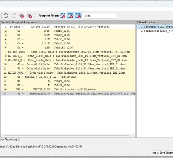 You can
filter footprints. By choosing the symbols and then clicking
one of the filtered footprints on the left, you assign them to the symbol. Do this for
all
of the components. Then press Apply&Save.
You can
filter footprints. By choosing the symbols and then clicking
one of the filtered footprints on the left, you assign them to the symbol. Do this for
all
of the components. Then press Apply&Save.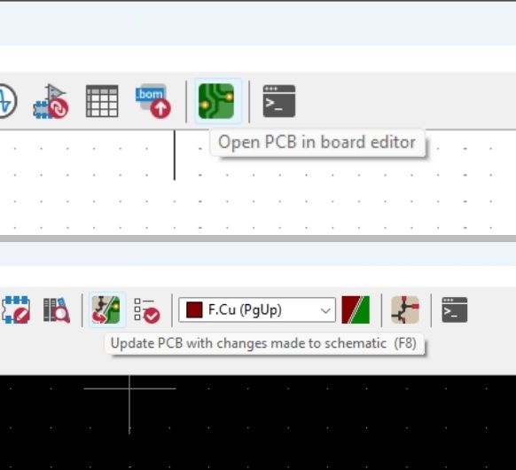 It's
finally time to create your pcb layout. Click this button in
your schema workspace to get to the pcb workspace. There, press the button to update
your
pcb with changes made to the schematic.
It's
finally time to create your pcb layout. Click this button in
your schema workspace to get to the pcb workspace. There, press the button to update
your
pcb with changes made to the schematic.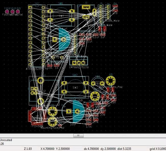 You will
get something that is roughly similar to this. A lot of
components with a lot of white lines. The white lines represent the logical connections.
You will
get something that is roughly similar to this. A lot of
components with a lot of white lines. The white lines represent the logical connections.
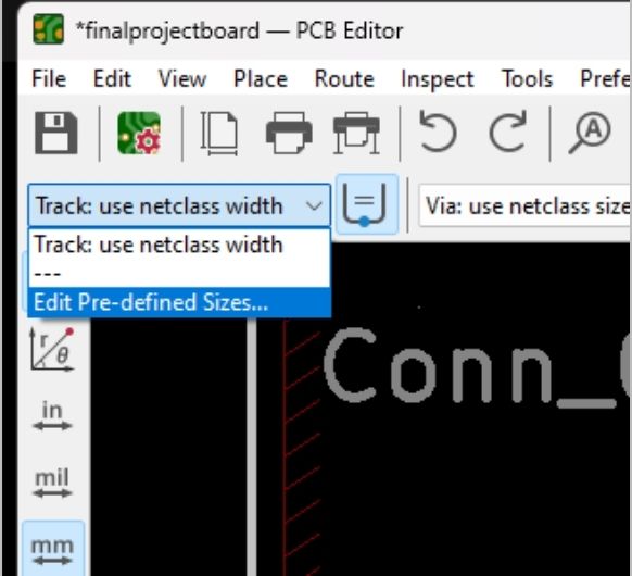 You might
want to change your track width before the wiring step. To
do so, click this button.
You might
want to change your track width before the wiring step. To
do so, click this button.
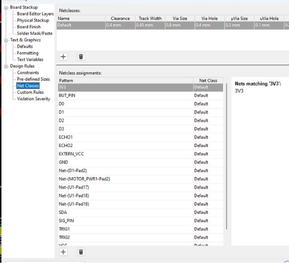 Go to Net
Classes. Here you can change the Clearance and the Track
width. Go with about 0.4mm minimum clearance and track width.
Go to Net
Classes. Here you can change the Clearance and the Track
width. Go with about 0.4mm minimum clearance and track width.
 You have
to turn the logical connections into physical ones using
the wire tool. You can layout your components by moving them with the mouse and then
drawing
wires between them, until all white lines disappear and everything is connectd the right
way. You can always go back to your schematic to change the logic if you realize you
made a
mistake or something doesn't fit. Just press update PCB afterwards and your changes will
be
applied.
You have
to turn the logical connections into physical ones using
the wire tool. You can layout your components by moving them with the mouse and then
drawing
wires between them, until all white lines disappear and everything is connectd the right
way. You can always go back to your schematic to change the logic if you realize you
made a
mistake or something doesn't fit. Just press update PCB afterwards and your changes will
be
applied.
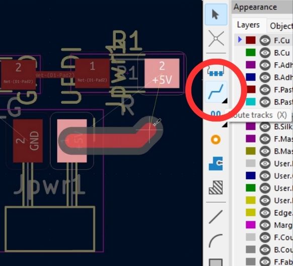
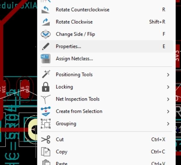 Another
best practice is to change the pad shape of the pin headers.
Usually they are round when you start out, but an oval like shape is often better. To
change, right click on any of the pads and choose Properties.
Another
best practice is to change the pad shape of the pin headers.
Usually they are round when you start out, but an oval like shape is often better. To
change, right click on any of the pads and choose Properties.
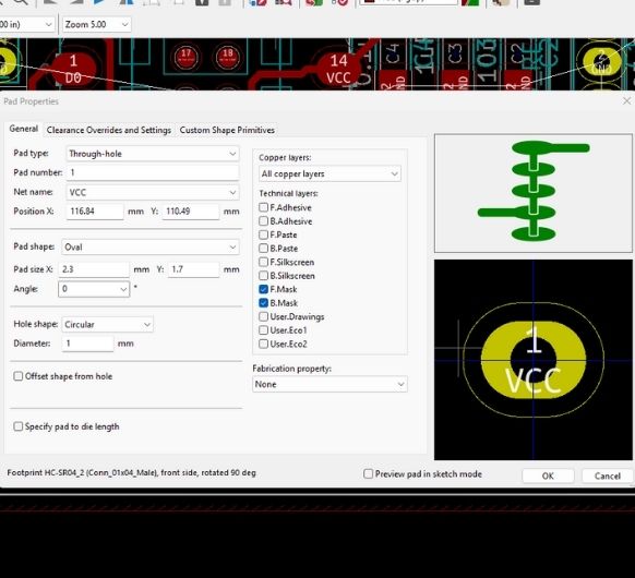 Change
whatever you have to these settings and apply.
Change
whatever you have to these settings and apply.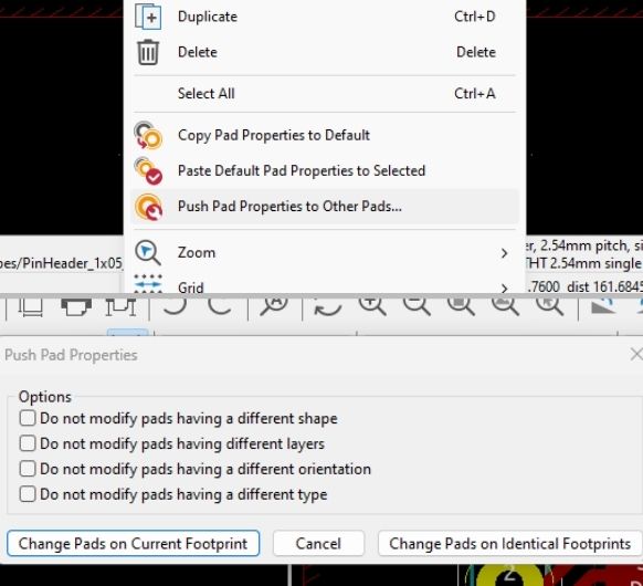 After
this you can copy the properties to all of the other pads.
After
this you can copy the properties to all of the other pads.
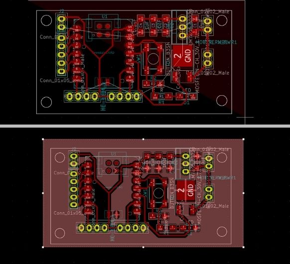
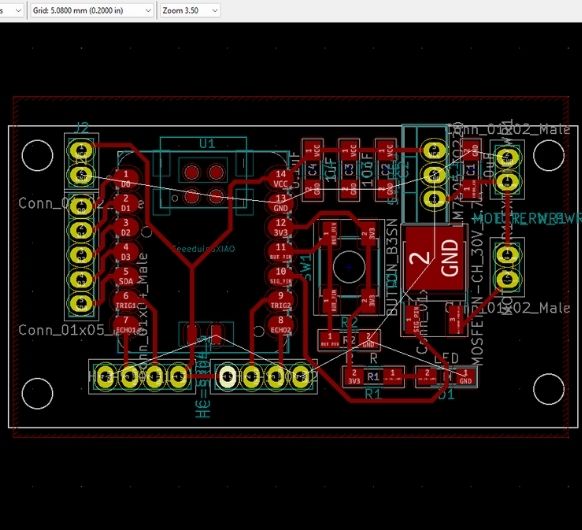 After
you are done arranging and wiring your PCB, it should look
something like this. But there's two more important things to note also visible on this
picture, a ground layer and an outline + mounting holes.
After
you are done arranging and wiring your PCB, it should look
something like this. But there's two more important things to note also visible on this
picture, a ground layer and an outline + mounting holes.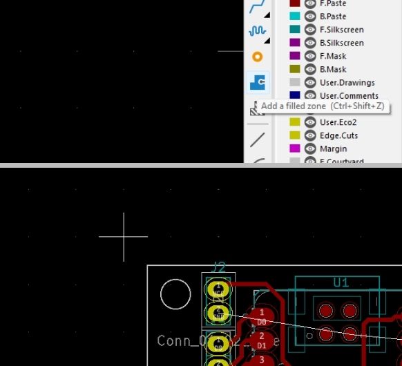 How to
make a ground layer: A layer that connects all GND's is super
useful as it saves you a ton of connections. Click on the Add a filled zone button and
click
where you want to start your filled zone.
How to
make a ground layer: A layer that connects all GND's is super
useful as it saves you a ton of connections. Click on the Add a filled zone button and
click
where you want to start your filled zone. 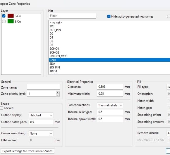 This
windows will pop up, choose GND and hit ok.
This
windows will pop up, choose GND and hit ok.
 Start
drawing your zone. When you are done, press B on your keyboard
to hatch it.
Start
drawing your zone. When you are done, press B on your keyboard
to hatch it. 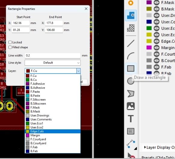 For the
outline, draw a rectangle around your PCB along with circles
for mounting holes. Right click on the lines and choose properties and change te Layer
to
Edge.cuts. And you're done!
For the
outline, draw a rectangle around your PCB along with circles
for mounting holes. Right click on the lines and choose properties and change te Layer
to
Edge.cuts. And you're done!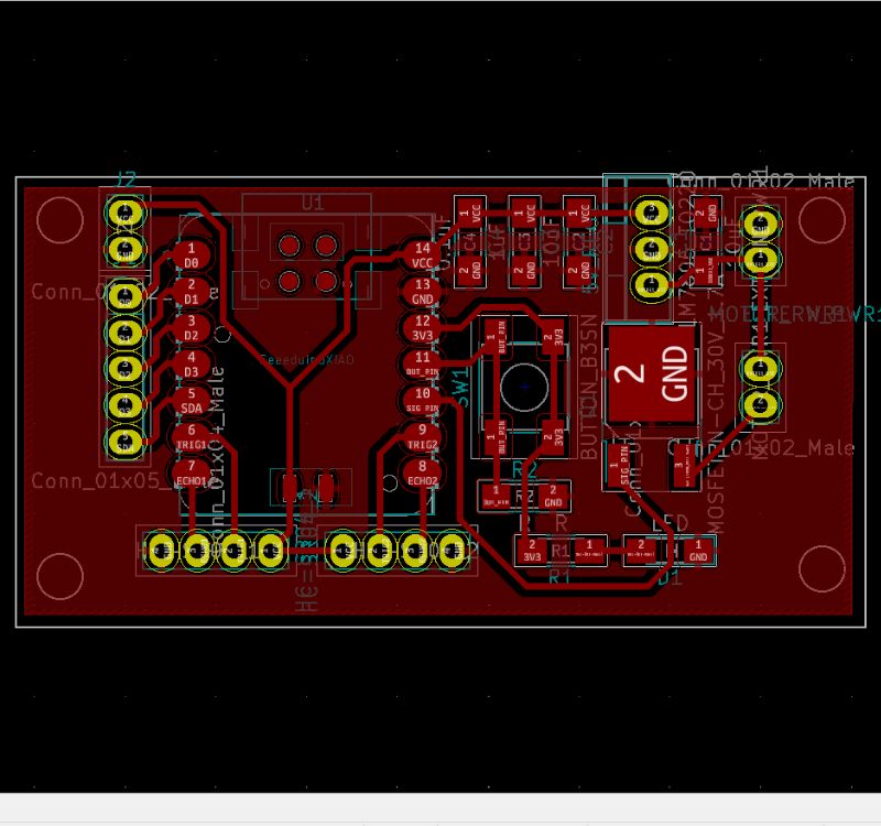 PCB
PCB Schema