


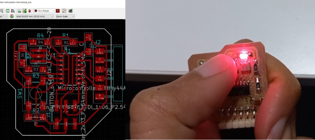
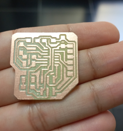
Here is my Hero-shot of the week! If someone told me a couple of years ago that I will be able to make a board that resembles Arduino I would have never believed! But here I am this week went through design, fabrication, soldering then coding a PCB board. So excited to see what I will be able to do in the next weeks as well.
Let's start first with the group assignment
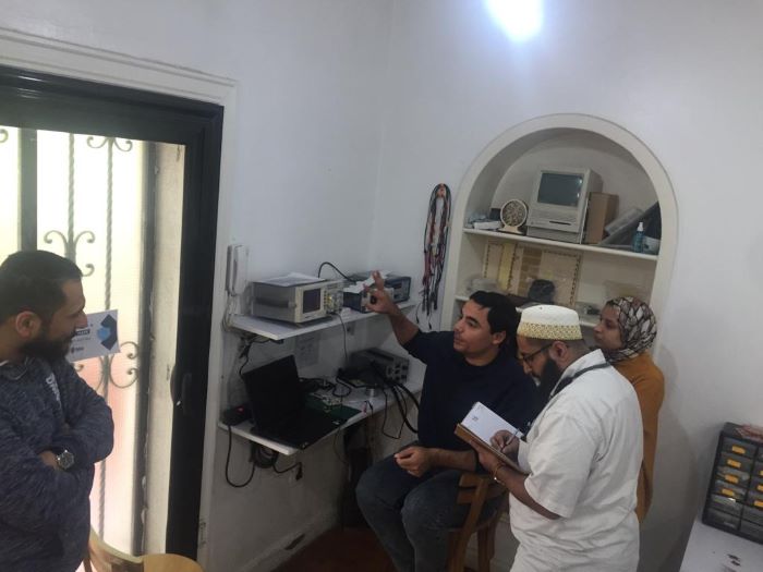
We started talking about different electronic components and how they behave and afftect the circuit they are in, Here is a photo that describes the basic elements of electronics Then our instructor Kamel had prepared a circuit board controlling a LED, where the microcontroller outputs a signal that makes the LED fades using PWM technique.
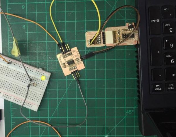
As you can see in the past photo we used UPDI progarmmer to program an Echo-Hello PCB which has Attiny1614 as a microcontroller. then through pin-headers connected to the MCU's pins controlled 1 of them to send a signal on the LED on a breadboard. Then connected the oscilloscope probes, 1 on the GND of our circuit and the 2nd with the +ve pin of the LED. then watched the signal being drawn as follows.
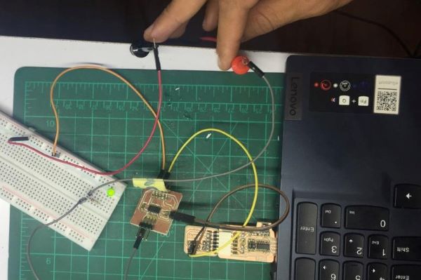
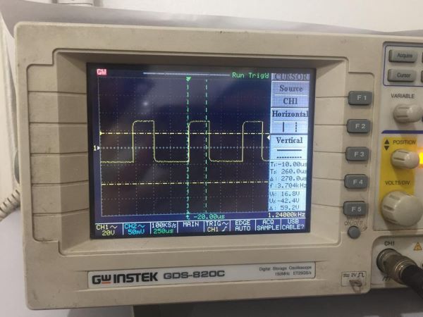
Then we tried different features of the oscilloscope which is a device that draws a graph of the instant voltage signal as a function of time. that's why we used oscilloscopein the first place, because the PWM signal changes over time. As for the signals that are constant like 5V DC we can use the AVOmeter to measure it. In the next video you will see the PWM signal changing and repeating itself over time.
Now, The assignment!
I already have a background using Eagle Autodesk software so decided to use a new one and see how my experience will be, so in this week I used Kicad.you can download itfrom here, make sure to download version 6 or later, will know why in a bit.
once I opened the program and created a new project the schematic environment looked familiar and easy to work with.
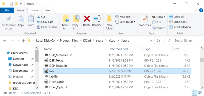
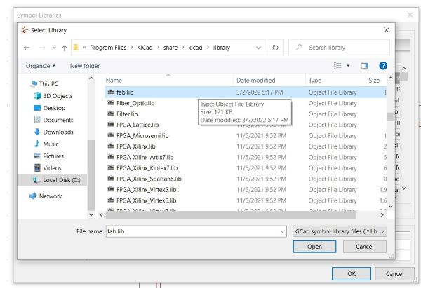
Then to be able to find all components easily I added fab library. you can download it from here I found libraries folder a bit deep inside not like the tutorial, its path was "C:\Program Files\KiCad\share\kicad\library" then I added just 2 files which are
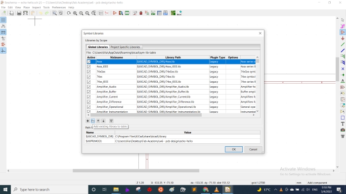
Then to be able to use it inside Kicad I went to prefrences then choose manage symbol libraries and then manually add fab.lib file
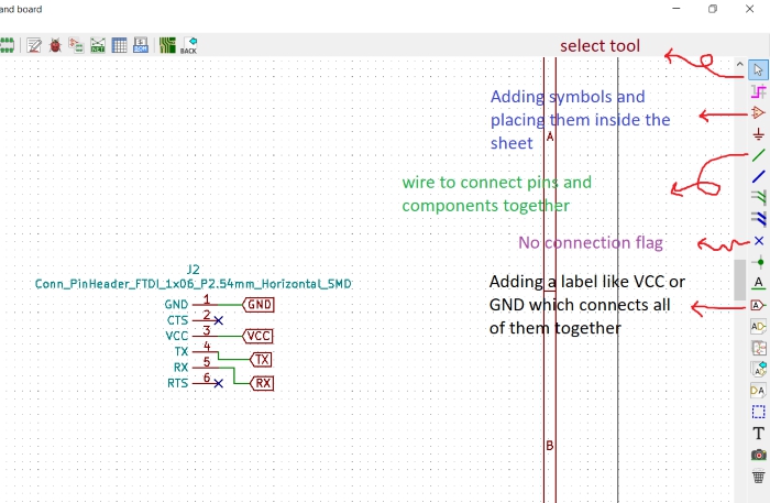
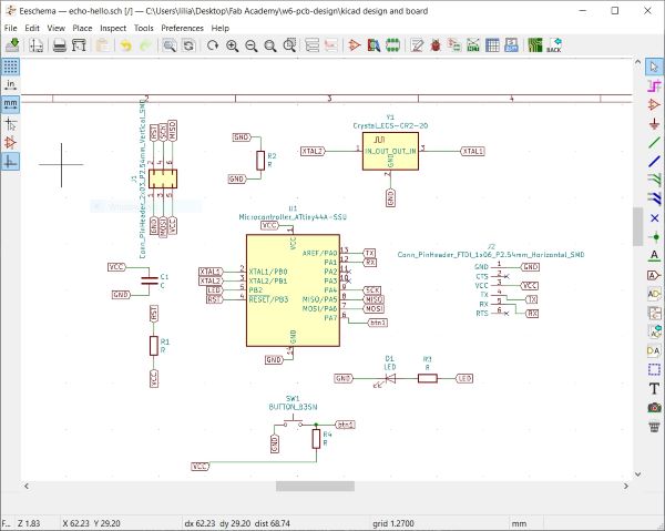
Then based on the original Echo-Hello PCB, I started to build my circuit, so added Attiny44 and other components' symbols using place symbol tool we talked about earlier. To be able to connect components I needed to see the datasheet for the Attiny44 to know which pins are used for ISP communication, VCC and GND pins..etc
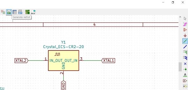
And so I managed to complete the schematic of my board, YAAY.
Then comes board design! but to be able to start with it we need to assign footprints to the symbols we choose on the schematic. so first I needed to add fab library for footprints too.
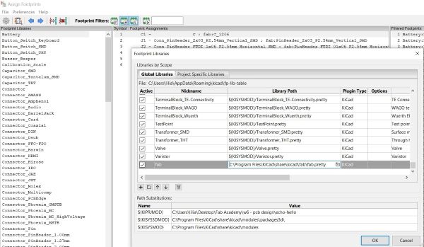
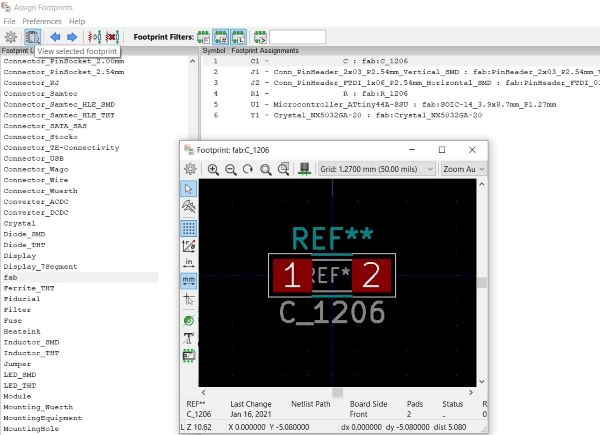
After that, started assigning each component to a footprint, you can see the footprint from this tool in the following picture.
Now that all is set in the schematic and did the footprint assigning, there is one last step, which is creating a netlist which is a file we save somewhere safe.
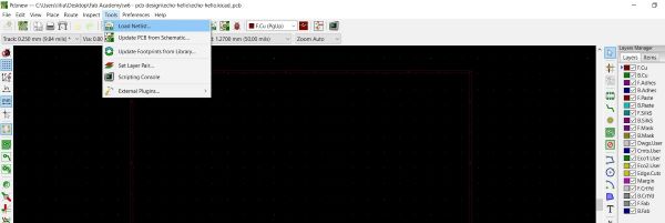
Then finally, clicking the button "Run PCBnew to layout printed circuit board" and the next window will show up. The board environment will be empty so we need to load the netlist that we saved to load the footprints and the connections from schematic file. from tools > load netlist that appears in the picture.
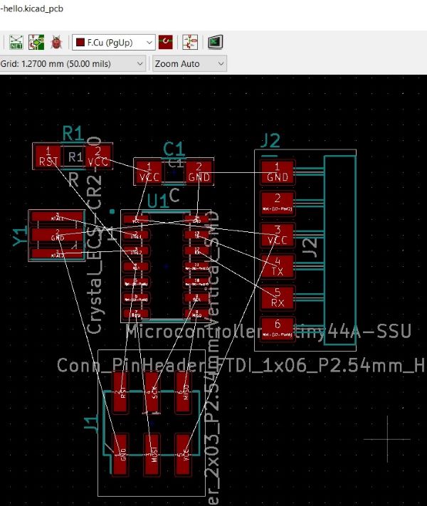
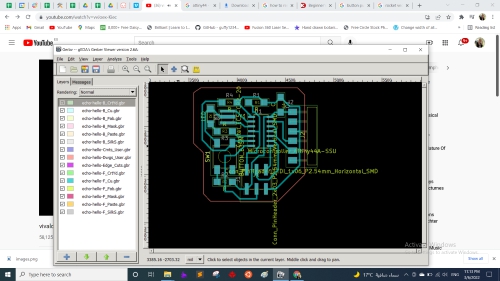
Then all footprints and connection will show up randomly like this
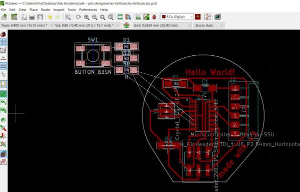
Now we need to move components and start wiring, so after a bit I thought I was done, at that time it looked like this:
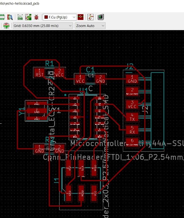
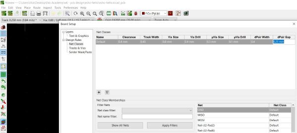
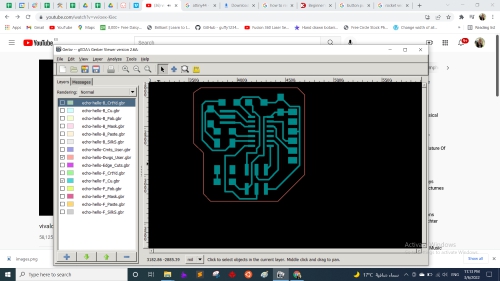
Before exporting any final files we need to do a Design Rules check, to see if all the traces and gaps between them will be proper for the CNC milling machine to mill, so from board setup we enter DRC values that we measured in the "PCB Production week" so for our Modela it was 0.4mm
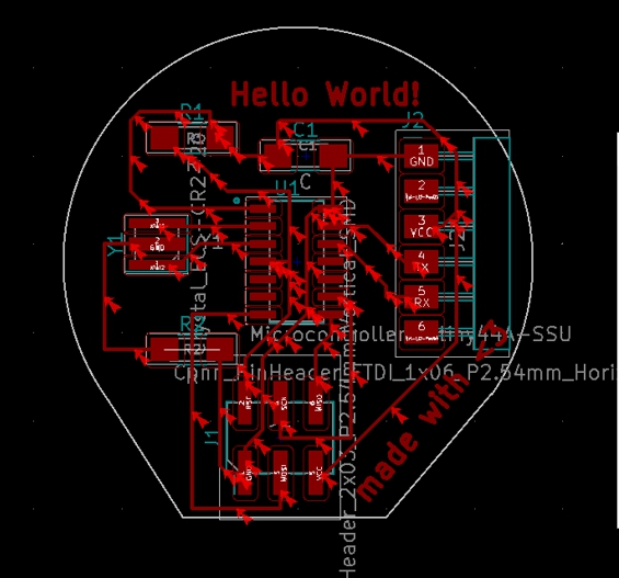
So I filled the values and hit check, I wish I didn't :D as all the traces I made was smaller than 0.4mm so the arrows pointed to all of them
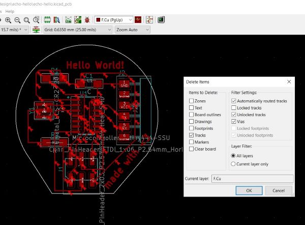
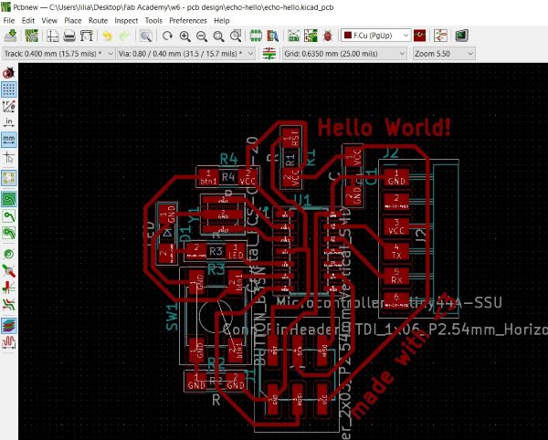
That's when I decided to delete all wires and make them all over again :D
It took less time than I expected then I added a push-button and a LED with resistors and edited the placing of some components a bit and finally done!
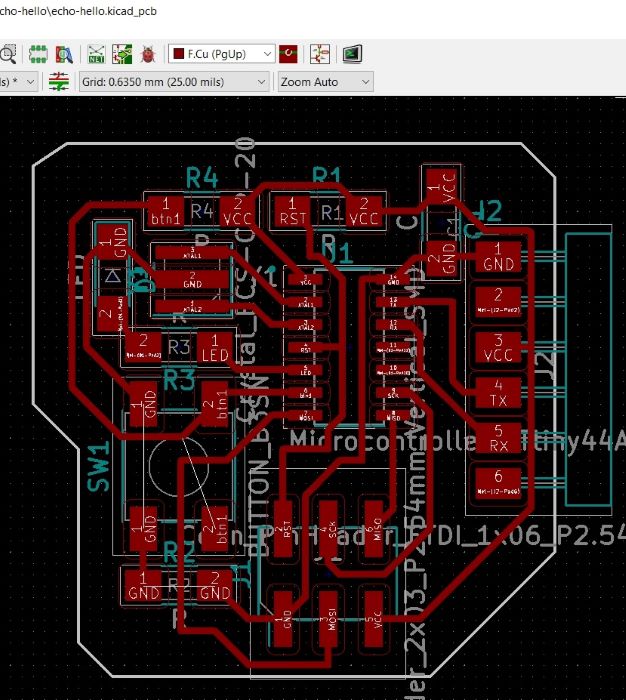
finally we need to draw an outline for the board so we either use "file>import graphics" to import a DXF design or we draw one using " add a graphic line/arc/circle" on the tools bar on the right. If you want to use a design please make sure to import it before doing the wiring and placing of components, as I added one after and it looked like i needed to do them all over again to make them fit inside the ready design. So eventually I used a graphical lines and drawn the outline with it. and WALLAH! finished.
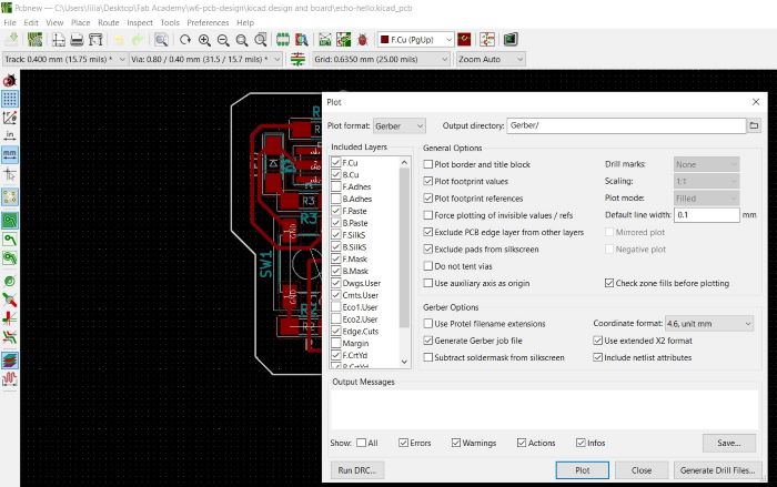
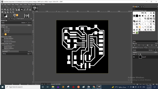
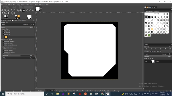
Then to be able to work with your design through PNG pictures you need to export it first into GERBER files, so from "plot" exported them.
to be able to convert gerber files to PNGs I needed to use gerber viewer software, so I used gerbv which exports PDF or PNG pictures. so after I opened the layer it looked like this, but those are all the layers in kicad inclusing silkscreen and soldermask we won't use so I unchecked all the not needed layers and what was left were top layer and outline, so colored them which black color and exported them into PDF.
Then used "GIMP" to export PNG pictures, So at then I was finally ready to fabricate the board!
The process of PCB milling went almost the same as "PCB Production week" and even easier this time, so after 45 mins I had this tiny beautiful PCB.
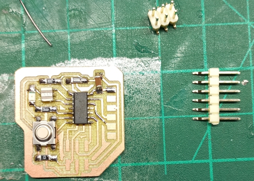
Then starteed soldering and stuffing components just like PCB Production week as well, from the center to edges and from down to up in height.
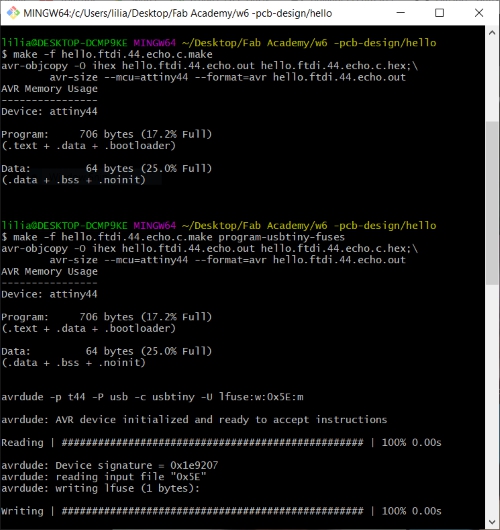
Finally comes programming! I used my FabISP to program it and use Neil's echo.c and echo.c.make files then followed the steps in the next picture which is attached in Fab Academy's assignment files as well.
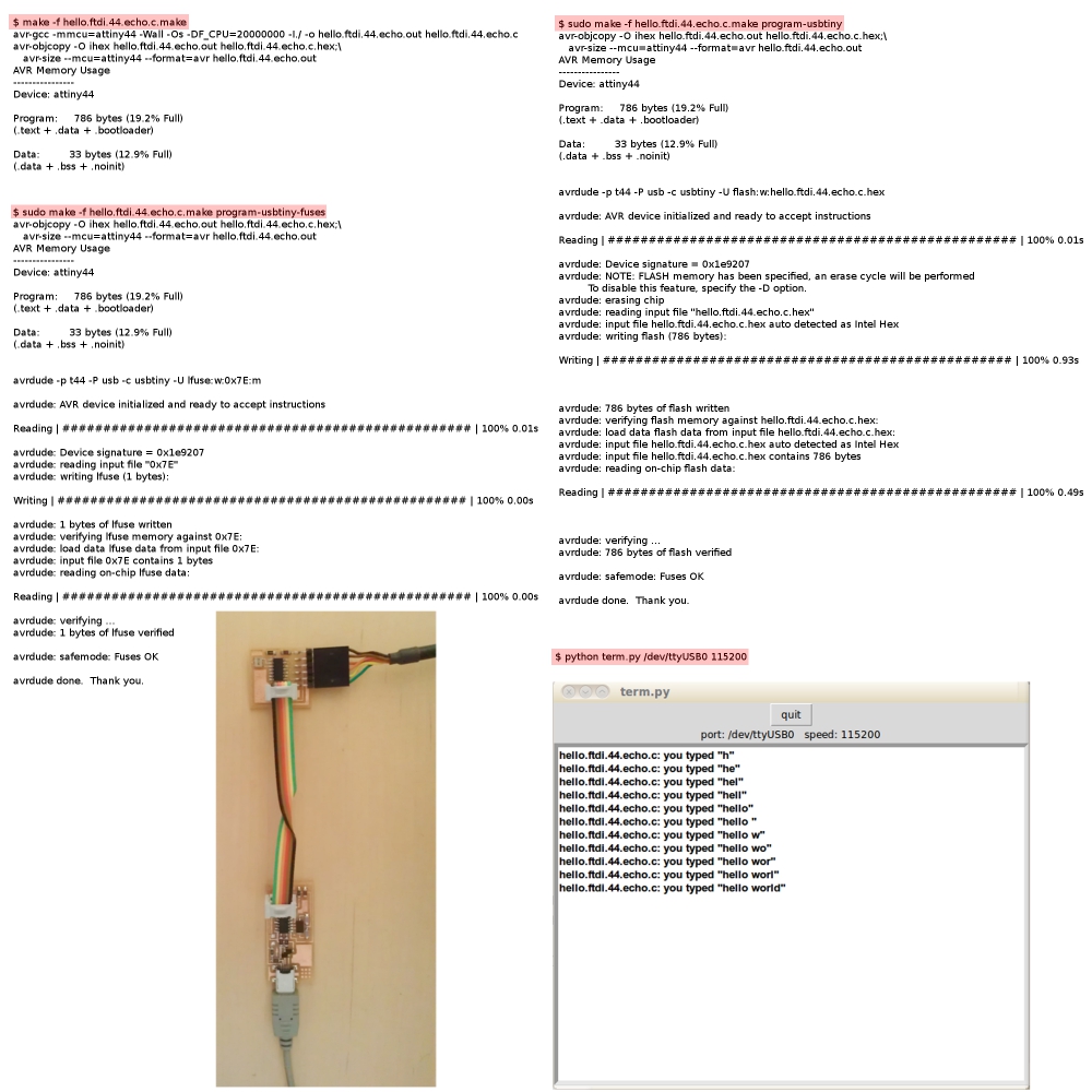
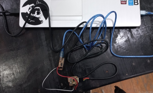
The connection was as follows, FabISP connected with my laptop through micro-USB cable, then FabISP and Echo-hello board connected together through ISP 6-pin protocol, then Echo-hello board connected with my laptop through FTDI cable. just like the next picture.
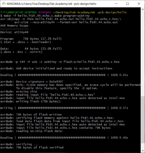
Then ran Git Bash from the folder that has Neil's "echo-hello.c and echo-hello.c.make" folder, then typed the same lines of the previous instructions picture. And yaaay! it worked from my first trial for once xD
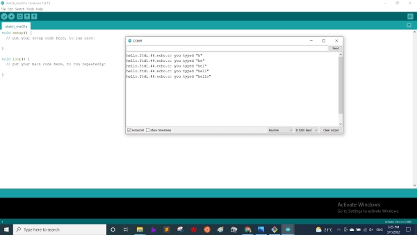
To test that the board is working well I opened Arduino IDE then without changing anything, just opened the serial monitor and made the baud rate 115200 then started typying letters and it echoed them! yay!
After that I wanted to test the led and the push-button as well so used a simple arduino code that makes the LED on when the push-button is pressed, otherwise is stays off. to be able to upload that program on the Attiny44 I used Arduino IDE for it and changed the board to Attiny44 and the programmer to USBtinyISP and then without burning bootloader I just clicked compile code and IT WORKED! I never been this happy to see a LED turned on and off :D
Source files:Individual Assignment files
Traces PNG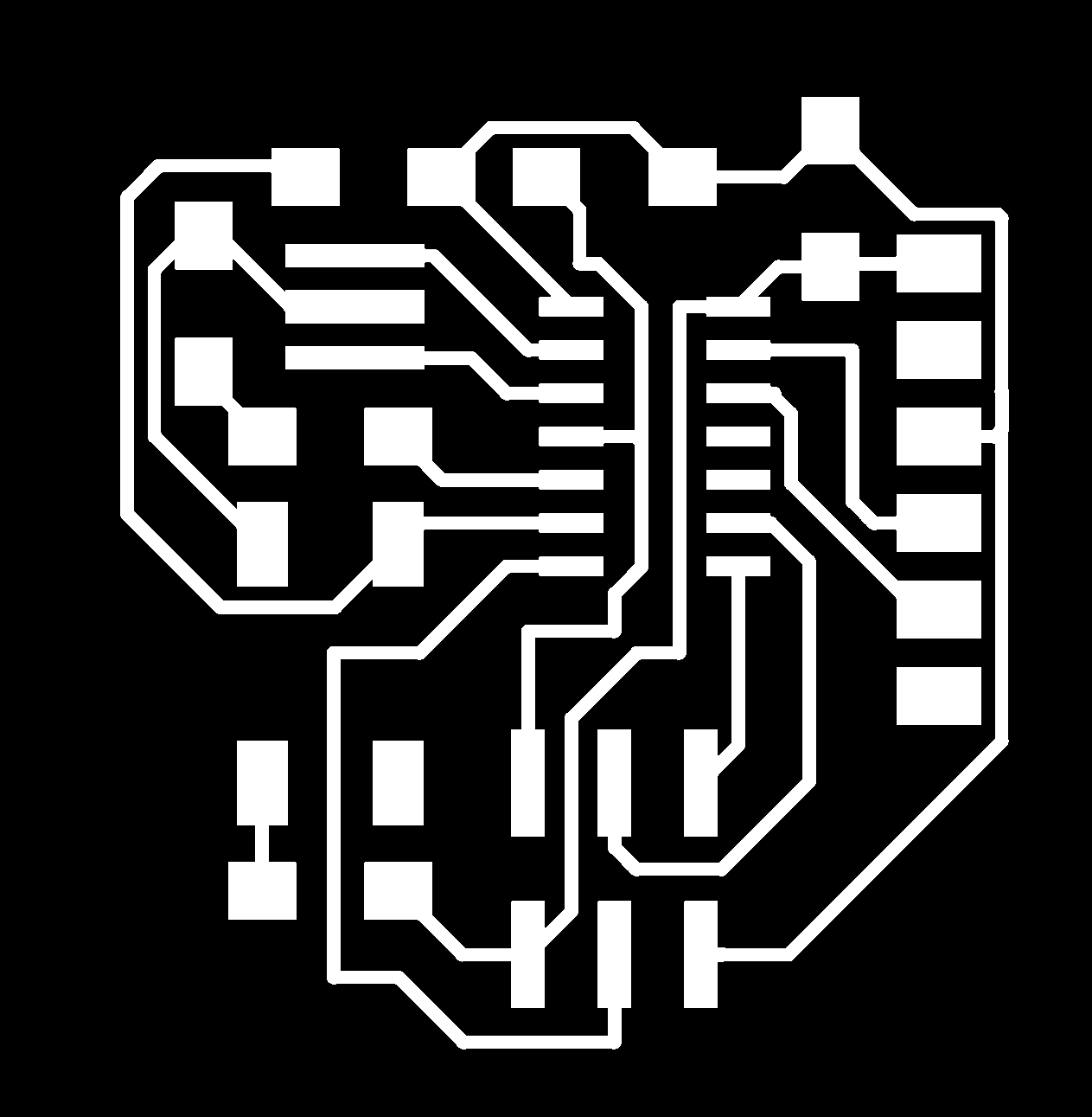
Outline PNG
Kicad project
Button-LED Arduino code