7. Electronics design
This week I worked on designing and build Print Circuit Board(PCB). One of dreams project is to build my own Arduino Board. To start I build an Arduino UNO board.
Group assignment:
- Use the test equipment in your lab to observe the operation of a microcontroller circuit board (in minimum, check operating voltage on the board with multimeter or voltmeter and use oscilloscope to check noise of operating voltage and interpret a data signal)
- Document your work (in a group or individually)
For the Group Work please check the Group Page for more details.
Individual assignment:
- Redraw one of the echo hello-world boards or something equivalent, add (at least) a button and LED (with current-limiting resistor) or equivalent input and output, check the design rules, make it, test it.
Tools I have used for this Project - EasyEDA
PCB Design
For PCB design I used EasyEDA which is an Easy and powerful online PCB Design tool.
Before start designing the PCB board check the Fab Lab Electronics inventory and select the components for this project. Datasheets can be found in https://www.digikey.com
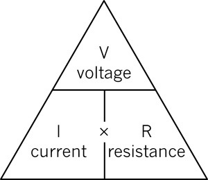
Ohm’s law
Ohm’s law is a relationship between the voltage, current, and resistance in any circuits.
LED Circuit
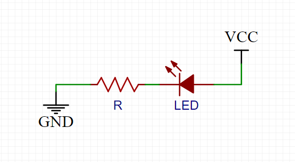
To find the right resistor for the LED check the LED Datasheet
- VCC = 5V
- LED Forward Voltage = 1.8V
- LED Forward Current = 20 mA
- R Voltage = VCC - LED Voltage = 3.3V - 1.8V = 3.2V
Now use Ohm’s law as following:
R = V/I = 3.2/0.02 = 160 Ω
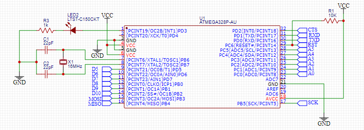
Microcontroller
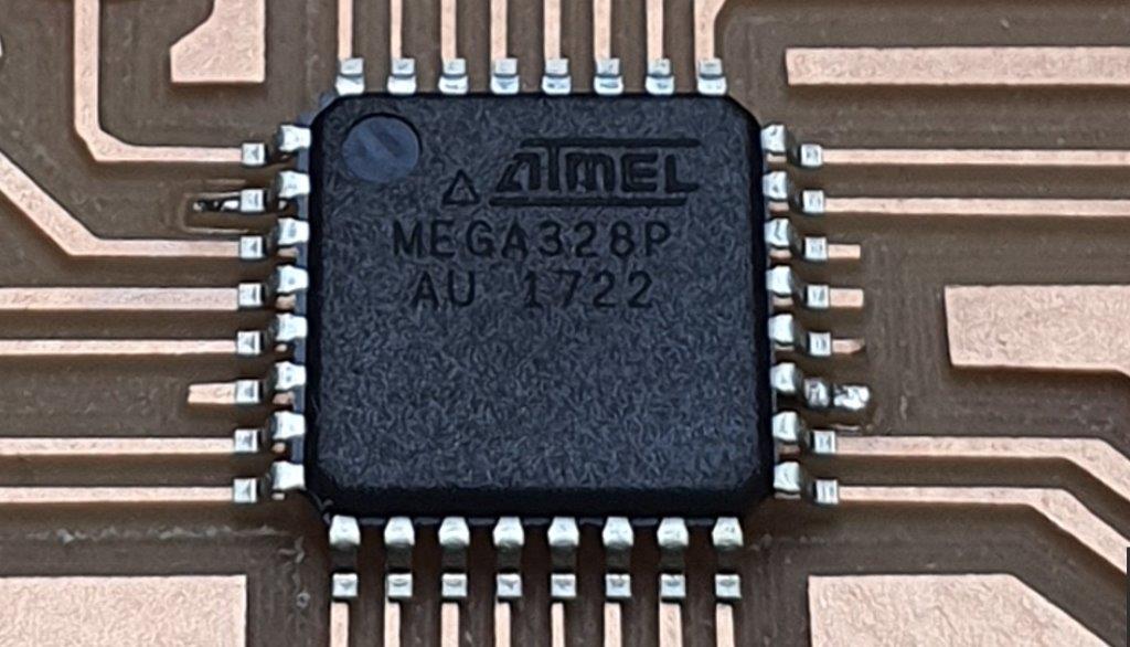 The microcontroller for Arduino UNO is ATMEGA328P which is a low power 8-bit microcontroller.
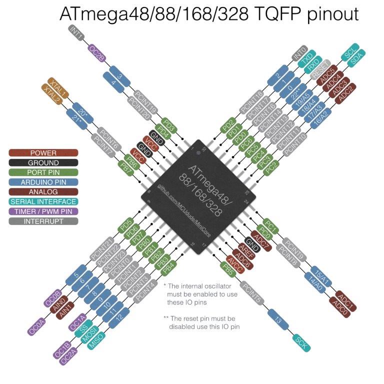
After reading the Datasheet here are some of the features:-
- PWM Channels: 6
- Program Memory Size: 32KB
- CPU Speed: 20 MIPS Throughput at 20MHz
- ADC Channels: 8
- Operating Voltage: 1.8 - 5.5
- Pin Count: 32
- SPI: 2
- Temperature Range: -40 - 85°C
Components:
Here the list of components I have used for this project
| ID | Name | Designator | Qty. | Datasheets |
|---|---|---|---|---|
| 1 | SMD_HEADER_1X8 | 1 | 1 | |
| 2 | 22pF | C1,C2 | 2 | |
| 3 | 10uF | C4,C5 | 2 | |
| 4 | 0.1u | C6 | 1 | |
| 5 | 210SMT-2*3P Gold-plated black | H1 | 1 | |
| 6 | FTDI-SMD-HEADER | H2 | 1 | |
| 7 | SMD_HEADER_1X6 | H4,H5 | 2 | |
| 8 | LTST-C150CKT | LED1,LED2 | 2 | Datasheet |
| 9 | 10K | R1 | 1 | |
| 10 | 1k | R2,R3 | 2 | |
| 11 | ATMEGA328P-AU | U1 | 1 | Datasheet |
| 12 | ZLDO1117G50TA | U3 | 1 | |
| 13 | 16MHz | X1 | 1 |
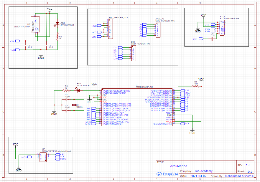
Schematic Diagram Start designing the PCB with the schematic diagram and place all the components you need the sketch.
As I’m making my own Arduino Uno design I have checked the official schematic design arduino-uno-smd-schematic.pdf and Arduino pinout for ATMEGA328P-AU
-
Start with the basic requirements for the ATMEGA328P-AU setup
-
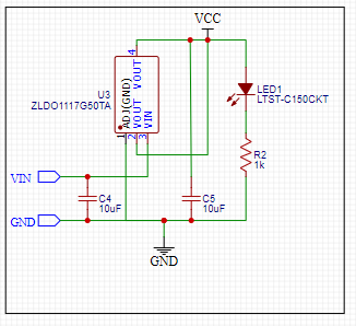
Create the Schematic for power module
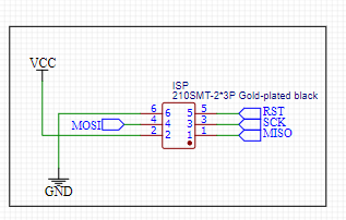
- Create the schematic for the ISP port
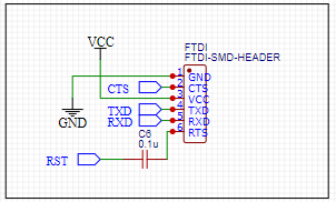
- Create the schematic for the FTDI Port
-
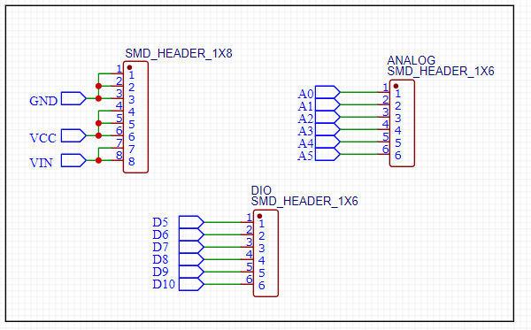
Create the schematic for IO Ports
-
Check the schematic Diagram
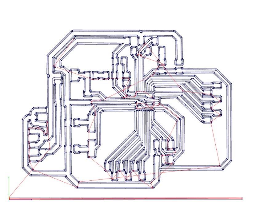
PCB
After finishing from schematic diagram design now time to design the PCB
- In EasyEDA go to File ==> New ==> PCB to create PCB project
- Then go Design ==> Import Changes to get all the Components and wire connections from the schematic diagram.
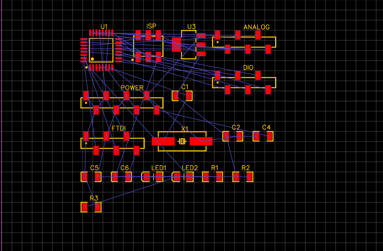
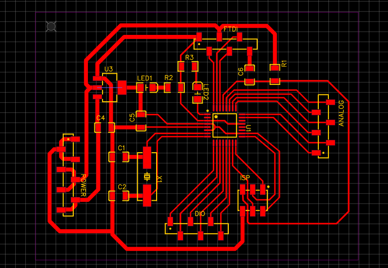
- Now move the components to their places and create the traces and try to NOT make 90 degree angle for the PCB track.
-
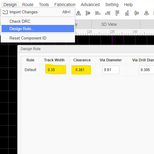
Set the Design Rule for the PCB Make the Track clearance “0.381mm” which is the minimum path for needed for the milling bit (1/64)
-
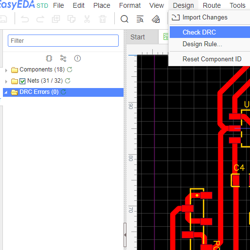
Go to Design ==> Check ERC and make sure you don’t have any error
-
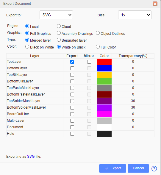
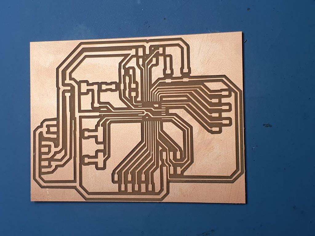
Export the TopLayer of the PCB design to SVG
-
Repeat the same step for the Outline
- Upload the files to fab modules and create the G-code. For more details please follow the instruction in Electronics production
Problem
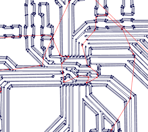
- Not able to get all traces for the ATMEGA328P-AU in fab modules, because of the pads size is 0.4mm
Solution
- Change the Pad width size from 0.4mm to 0.35mm and repeat the the above steps again.
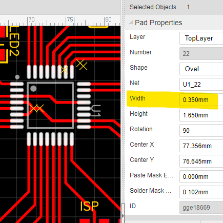
- Now I got nice traces lines in fab modules
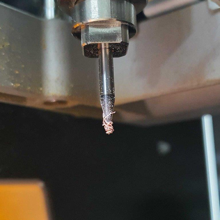
PCB Production
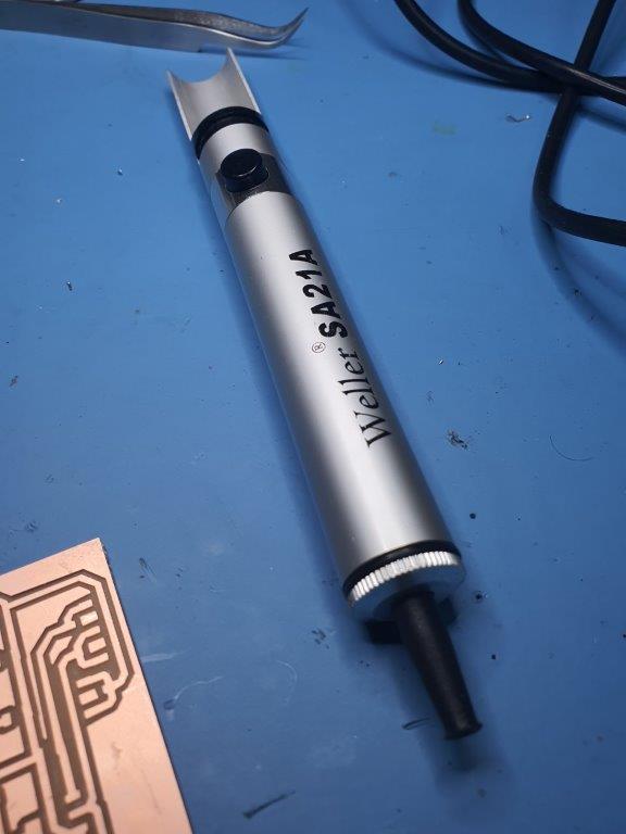
For PCB production I have used the Desktop Milling Machine Roland SRM-20 and follow the instruction in Electronics production
-
Problem: After follow the instruction in Electronics production and finished the cut I found that some cobber stuck to milling bit and destroy all the small traces for ATMEGA
-
Solution: Check the milling bit with microscope before start cutting
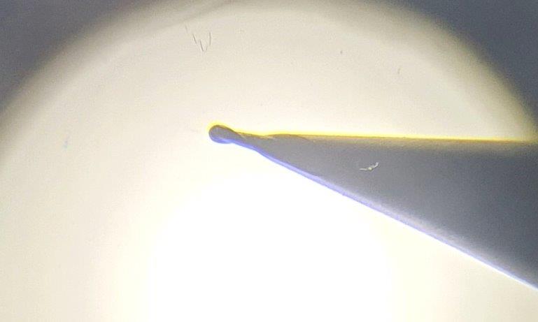
-
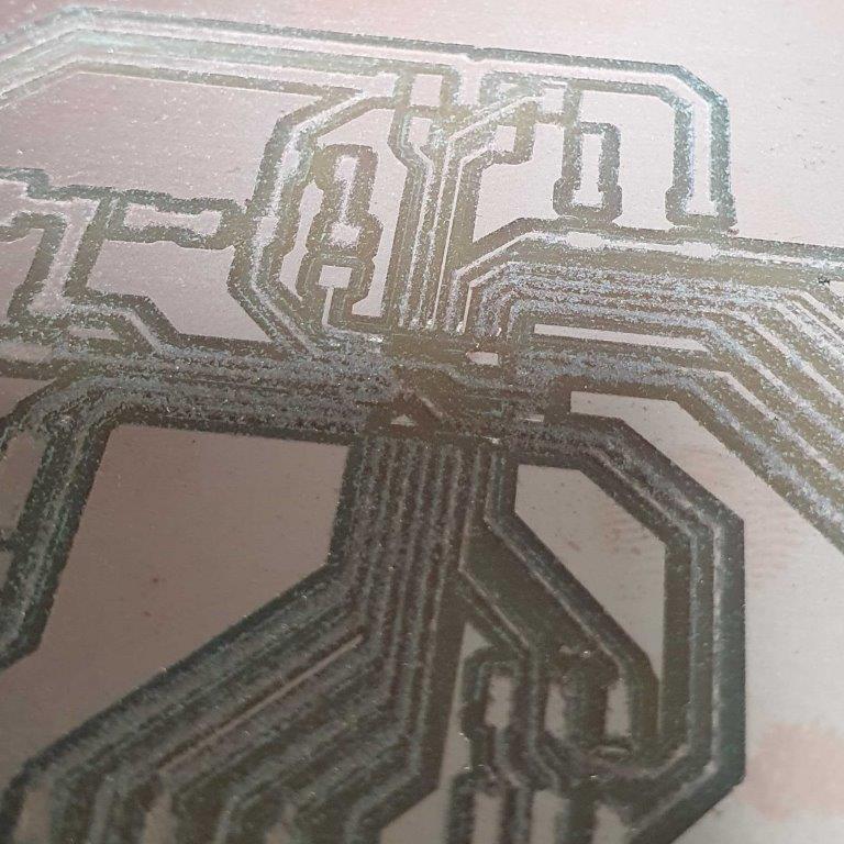
Now I got nice and clean PCB Board
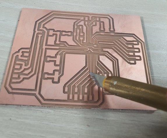
- Use Knife Cuter to remove extra copper
- Start soldering with the microcontroller first
- Issue I have soldered two pads together
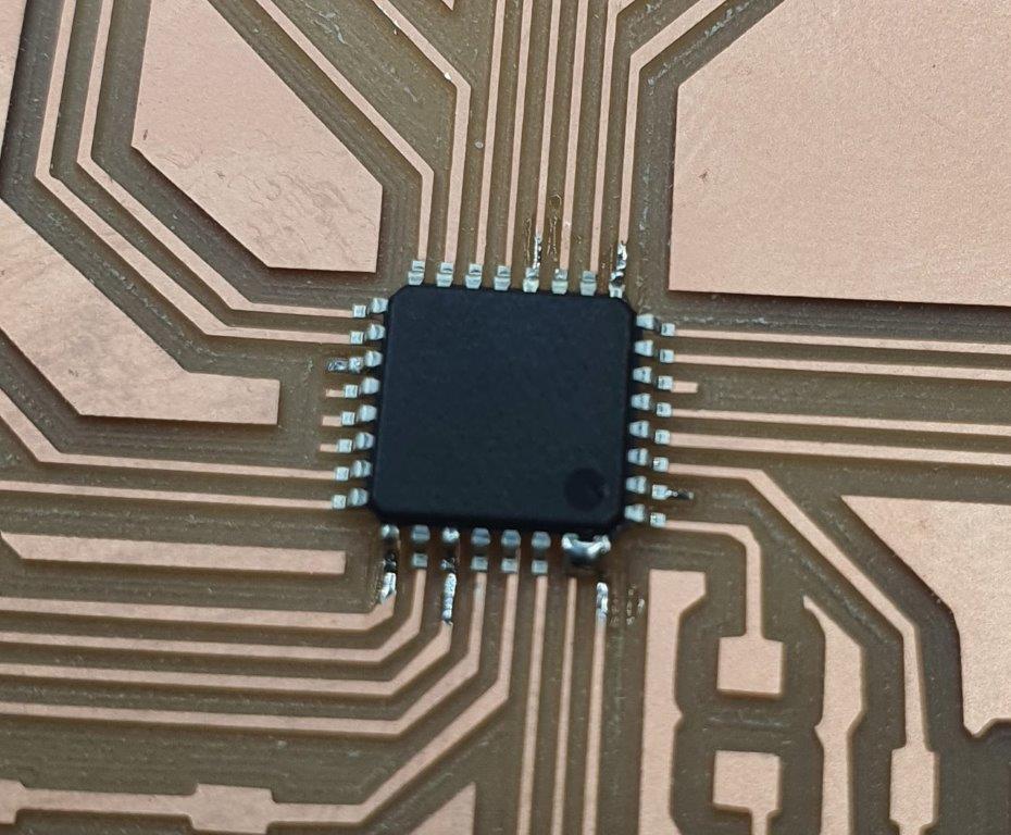
- Solution: Use DESOLDERING SUCKER to remover the extra solder
- Now solder the reset of the components
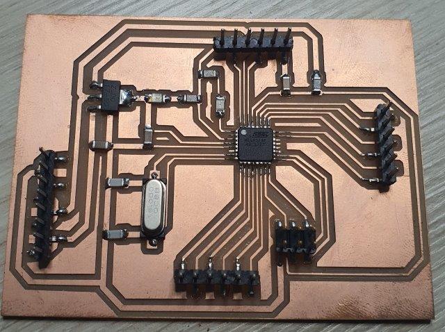
Final Result
Here is the video for the final result
It was very exciting moment when I sea the LED start blinking.