5.Electronics production
please download the files for this week before you start

![]()
Introduction:
This week We worked on producing FabTinyISP, the FabTinyISP is version of an AVR ISP programmer/board , we can produce FabTinyISP in any Fab lab using milling machine and available components in Electronics inventory , for this week I used monoFab SRM-20 by Roland.
![]()
Reference 1: Zaerc’s FabTinyStar
Reference 2: Building the FabTinyISP
![]()
- This version (the “FabTinyISP Minimal” is a minor revision to Zaerc’s version 0.3 (Bas), with small modifications:
- The reset switch and target power switch have been removed. The reset switch adds cost and isn’t incredibly useful on an ISP programmer, as the target can be easily reset through a software command. The target power swtich has been removed as providing power to the target through the programming port is usually discouraged. Users who understand the implications of this are welcome to build one of the FTS designs with the switch.
- The copper ground pour has been removed and replaced with individual ground traces; this allows novice solderers to mill away more of the copper. All components solder to clearly defined pads on both sides
- The extra pads connecting to the USB data lines were removed; this version is targeted solely at being an ISP programmer rather than being a general-purpose tiny45 board. The PTC thermistor was removed; as this part currently isn’t in the inventory most users would build it with a 0Ω resistor anyway. As the option to provide target power has been removed, it should be much more difficult to create a condition where the polyfuse would be needed.
- The Makefile has been replaced. Targets for programming the fuses on an ATtiny45 have been added. The original Makefile also results in problems on case-insensitive filesystems (i.e. Windows).
![]()
![]()
Electronics production stages
To do list : - [x] PCB Design - [x] Assembling the PCB - [x] Check Your Work - [x] Software Installation - [x] Get and Build the Firmware - [x] Program the ATtiny45 - [x] Test the USB Functionality - [x] Blow the Reset Fuse - [x] Test Your Programmer
![]()
![]()
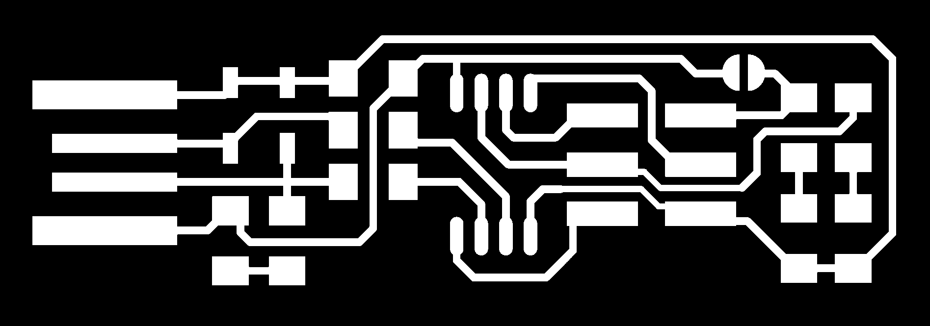
PCB Design
Introduction
A good and well-tested PCB design is always the way to a smooth Fabrication process.
PCB designers usually start with a schematic drawing that has parts based on the PCB required function “ISP programmer for AVR microcontrollers”
Example

The original schematic from simpleavr.com
![]()
process
Step 1 : after you draw you schematic you should Redraw it using PCB Design software like Eagle

Step 2 : after you draw you schematic using Eagle you turn it to PCB Design

these two images are super important because we are going to use them while we debug our assembly
what you can understand and read of this drawings :
1.the parts
2.parts location
3.parts orientation
4.parts Conductive trace
![]()
notes
- This version (the “FabTinyISP Minimal” is a minor revision to Zaerc’s version 0.3 (Bas), with small modifications:
as FabTinyISP is a “low-speed” USB 1.1 device. This is the slowest (and one of the oldest) of the USB device types. Typically used for mice and keyboards, low-speed devices operate at 1.5MHz and have much less strict timing requirements, which enables a purely software-based implementation of the USB protocol to be used (the ATtiny45 does not have hardware USB capability).
usually if you have a new laptop it has low speed USB on the left side of it the right side usually has the advanced USBs so connect you FabtinyISp using the lowest speed USB you have
![]()
![]()
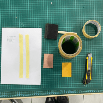
PCB Fabrication
Introduction

Size: 451.0 (W) x 426.6 (D) x 426.2 (H) mm
Max cutting area: 232.2 (X) x 156.6 (Y) mm
Power: Machine: DC24V, 2.5A,
Dedicated AC adapter: AC 100-240V ±10%, 50/60Hz
Included items: USB cable, AC adapter, Power cord, Cutting tool, Collet, Set screw, Spanners (7,10mm / 0.28, 0.39 inches), Hexagonal wrench (size 2,3 mm / 0.059, 0.12 inches), Positioning pins, Double-sided tape, Start-up page guidance card
Safety First : check the connection and safety cautions and bits covers

process
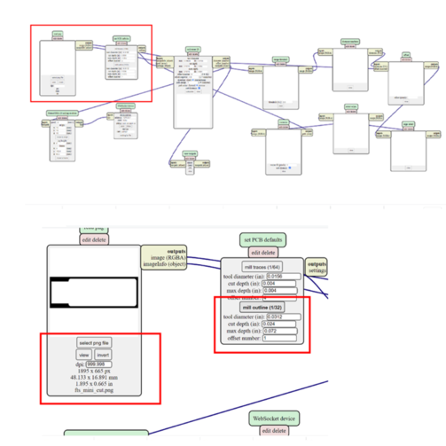
Step 1 : after you are done with PCB design you should be able to export traces” and cut .png files

Step 2 : File Download
for the inner traces

Trace width test “traces” png file
for the outer cut

Trace width test “cut” png file
Step 3 : use mods to generate the rml files from png images. The .rml extension is needed for the Roland machine.
Step 4 :
right click *
chose programs then open server program then the machine you use ” in our case SRM-20”
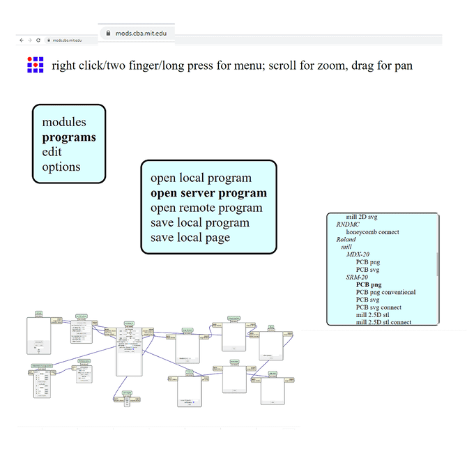
Step 5 : upload both .png

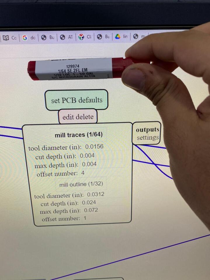
Step 6 : for the traces we use the (1/64)inch .04 m and then change the offset so you can get the cleanest cut the bigger the number the better ,though -1 well remove all the extra lines
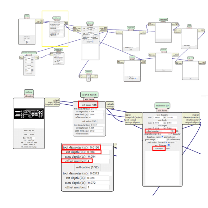
Step 7 : change the XYZ to 0 rather than 10 usually 10 is a default for safety but if you are sure of your design use zero
Step 8 : press calculate

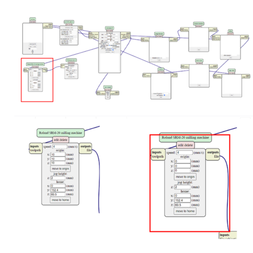
Step 9: the original mods use send to and you can use it if you use lennox but if you are using other OS you need to create a save node
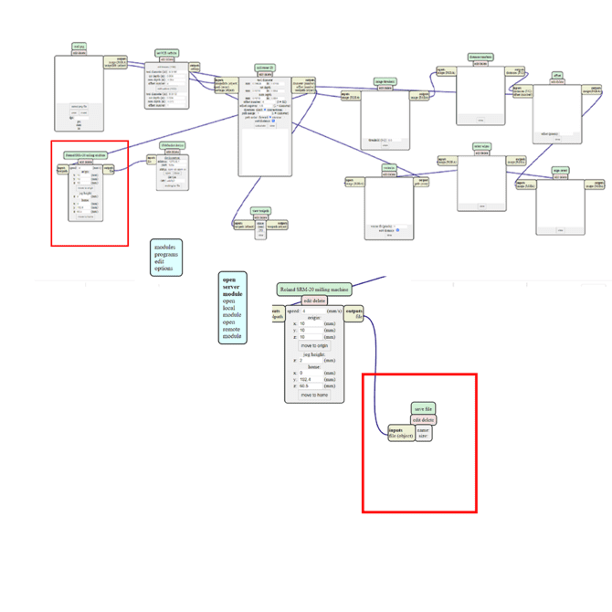
Step 10 : Download the .rml file for the traces png and then redo the whole process for the cut png though you need to chose 1/32 milling bit and always make sure that the DPI matches in both png and the size is logical then Download the .rml file for the cut file
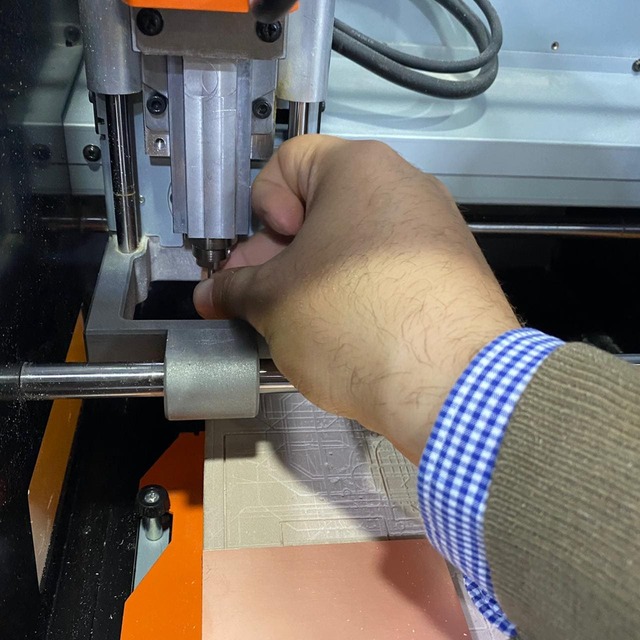
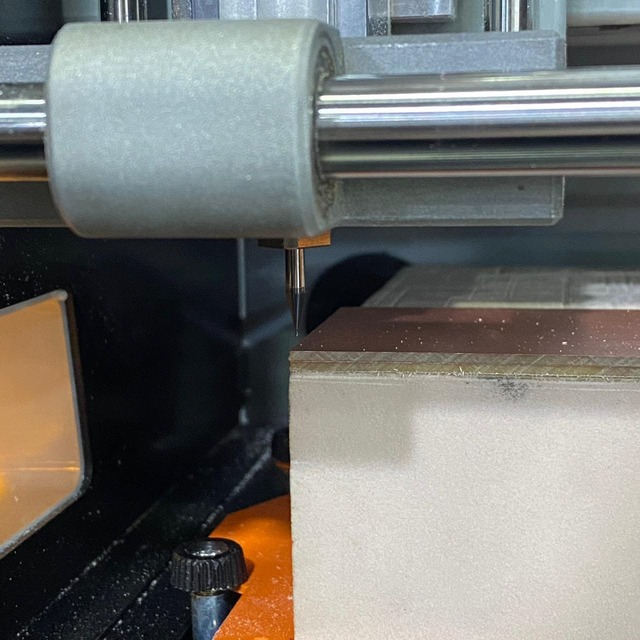
Step 11 : now after we prepared the CAM files We will adjust the machine and start cutting
Step 12 : open the machine and take off the bed so we can place the PCB on it
remove the bed
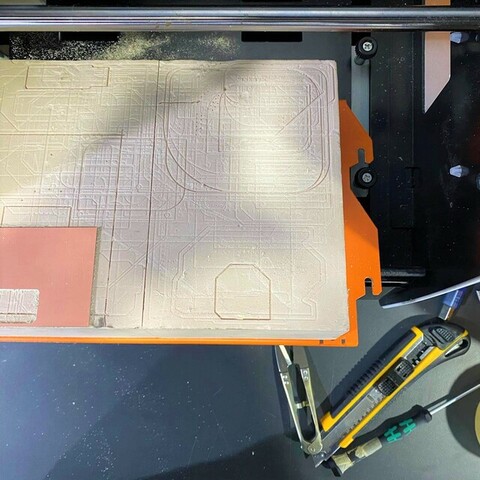
use the double sided tape and cover the back of the PCB
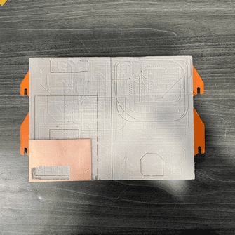
using the following tools
place it in needed place after cutting the extra tape
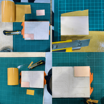
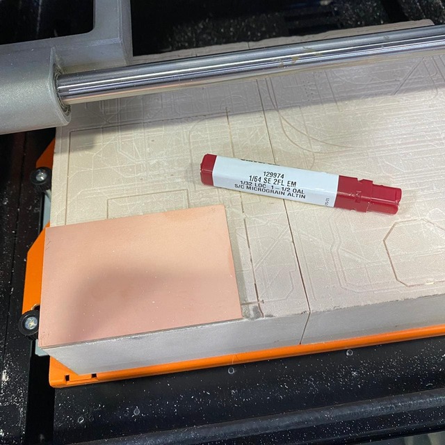
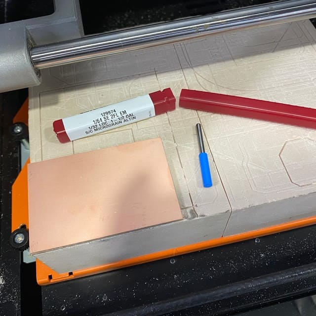
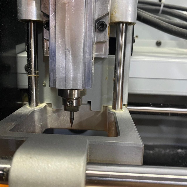
Step 12 :Job consists of two parts; First the milling of traces. For this part we used the traces png file and 1/64” (0.4 mm) milling bit. Second the cutting of the interior. For this part we used the interior png file and 1/32” (0.8 mm) milling bit.

milling bits assembly
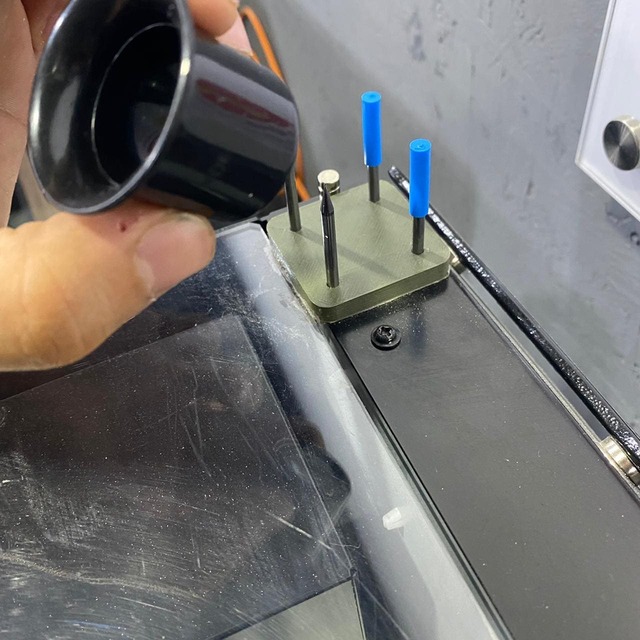
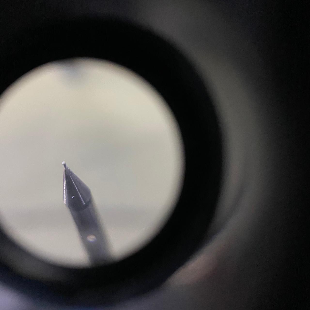
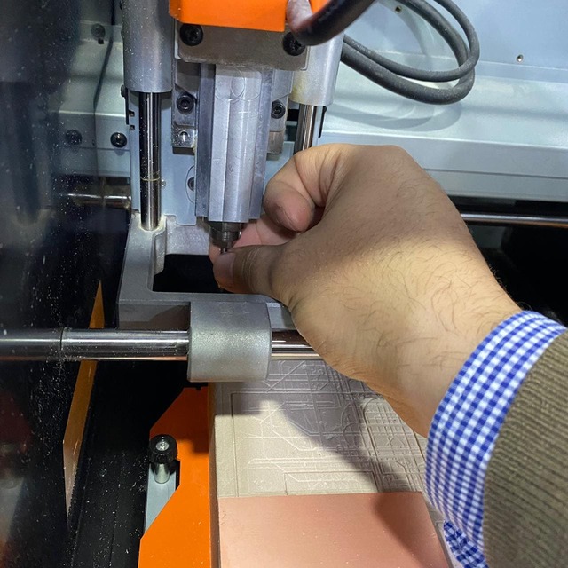
Step 1: Insert the 1/64” milling bit in the spindle collet leaving about 25% of its length outside. Tie the fixing screw.
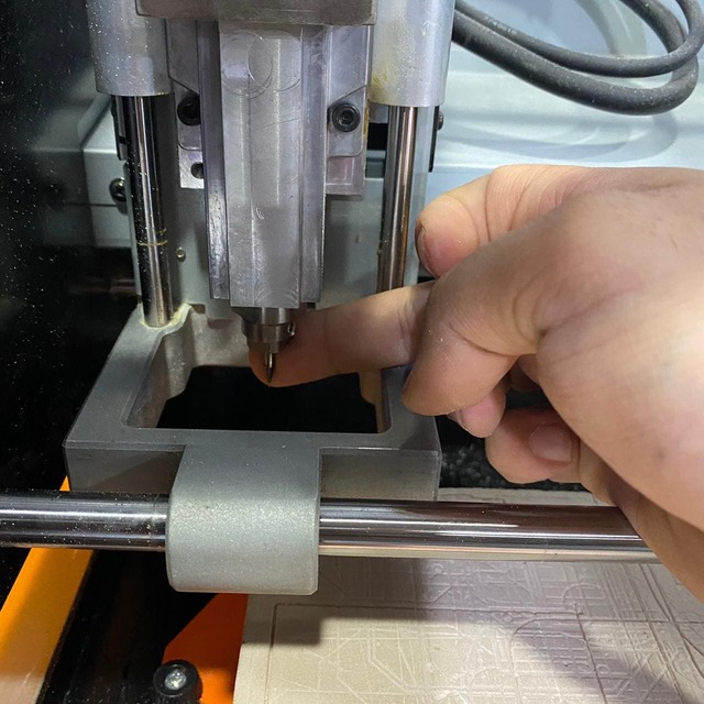
open VPanel for SRM-20 software
we will use the rml files to mill and cut the PCB. Before we start we need to set the origin of the mill bit by adjusting its relative position.
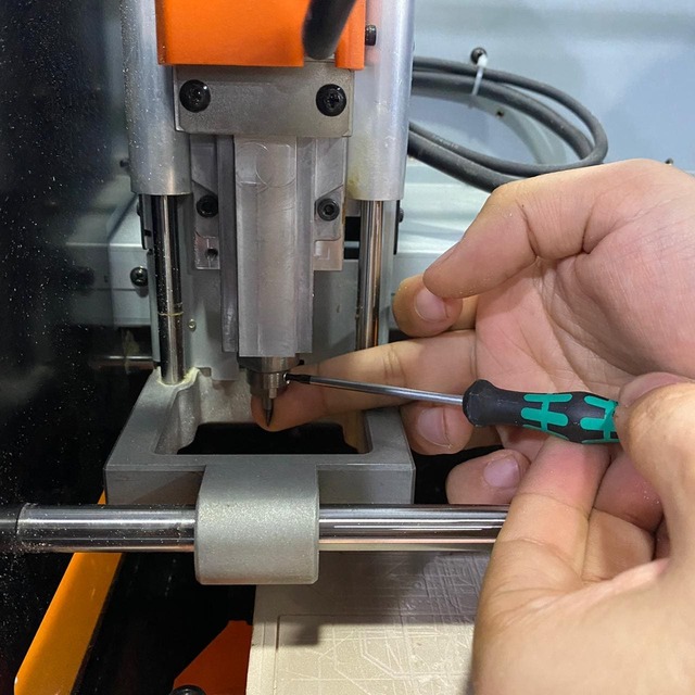
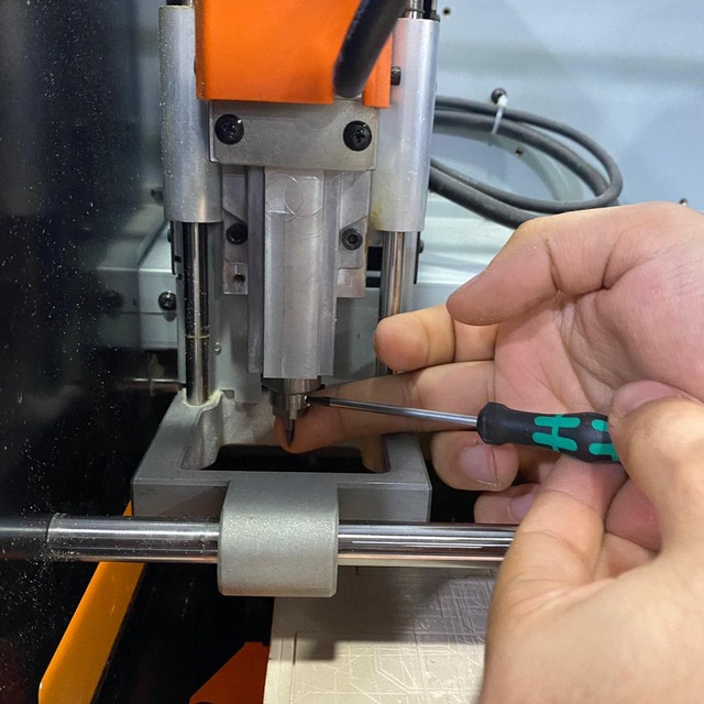
Step 2: Use the “+X, -X” and “+Y, -Y” arrows to move the head over the bottom left corner of the PCB. Use the “+Z” arrow to have enough space between the spindle and the PCB to insert the milling bit.
Step 3: Using the “-Z” arrow, move the spindle down till there is about 5 mm between the PCB and milling bit tip. Hold the milling bit between your fingers and untie the fixing screw. Move the milling bit down till it touches the PCB. Tie the fixing screw firmly. This is your home position.
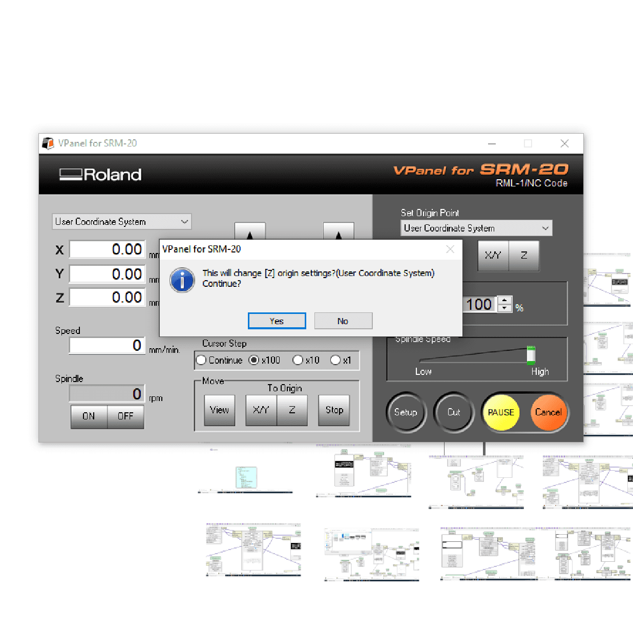
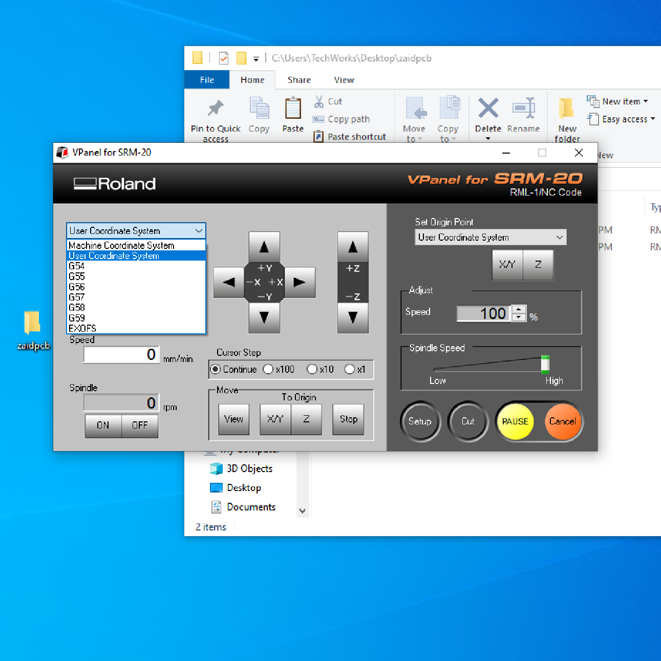
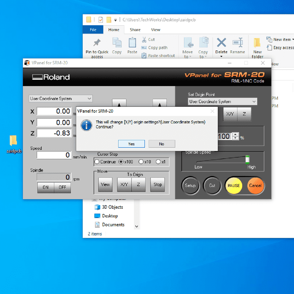
Step 4: From the “Set Origin Point” dropdown menu to the right, make sure to select “User Coordinate System”. Click on “XY” and “Z”. This will define the current position as the home or zero position in the user coordinate system. Select “User Coordinate System” from the dropdown menu to the left. The values of “X”, “Y”, “Z” should be zeros.
Step 5: Using the “+Z” arrow move the milling bit a few millimeters above the PCB, so that when the spindle starts it won’t be touching the PCB.
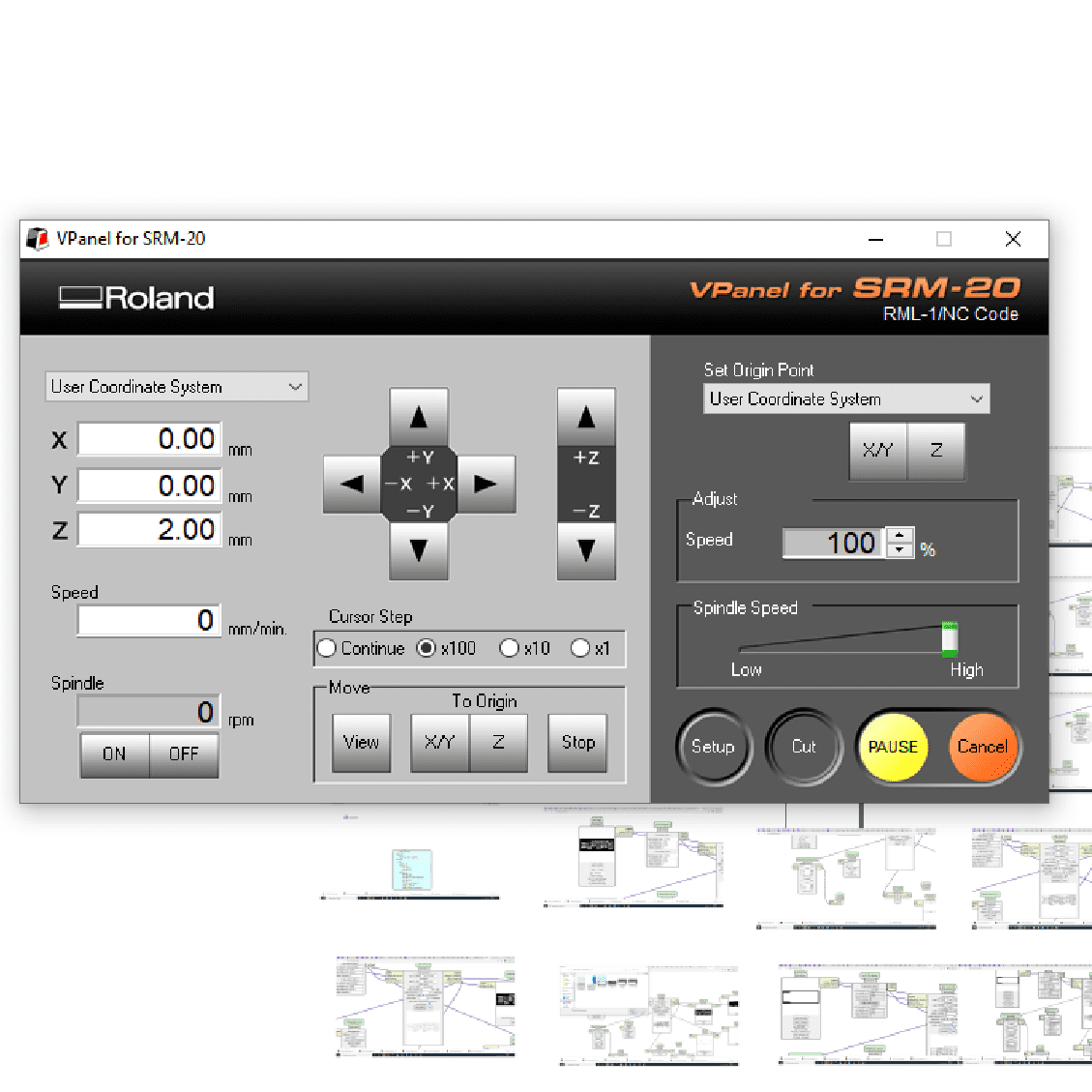
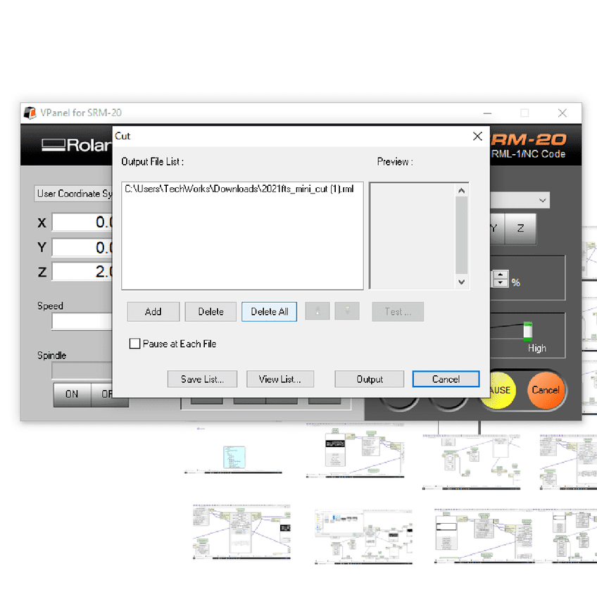
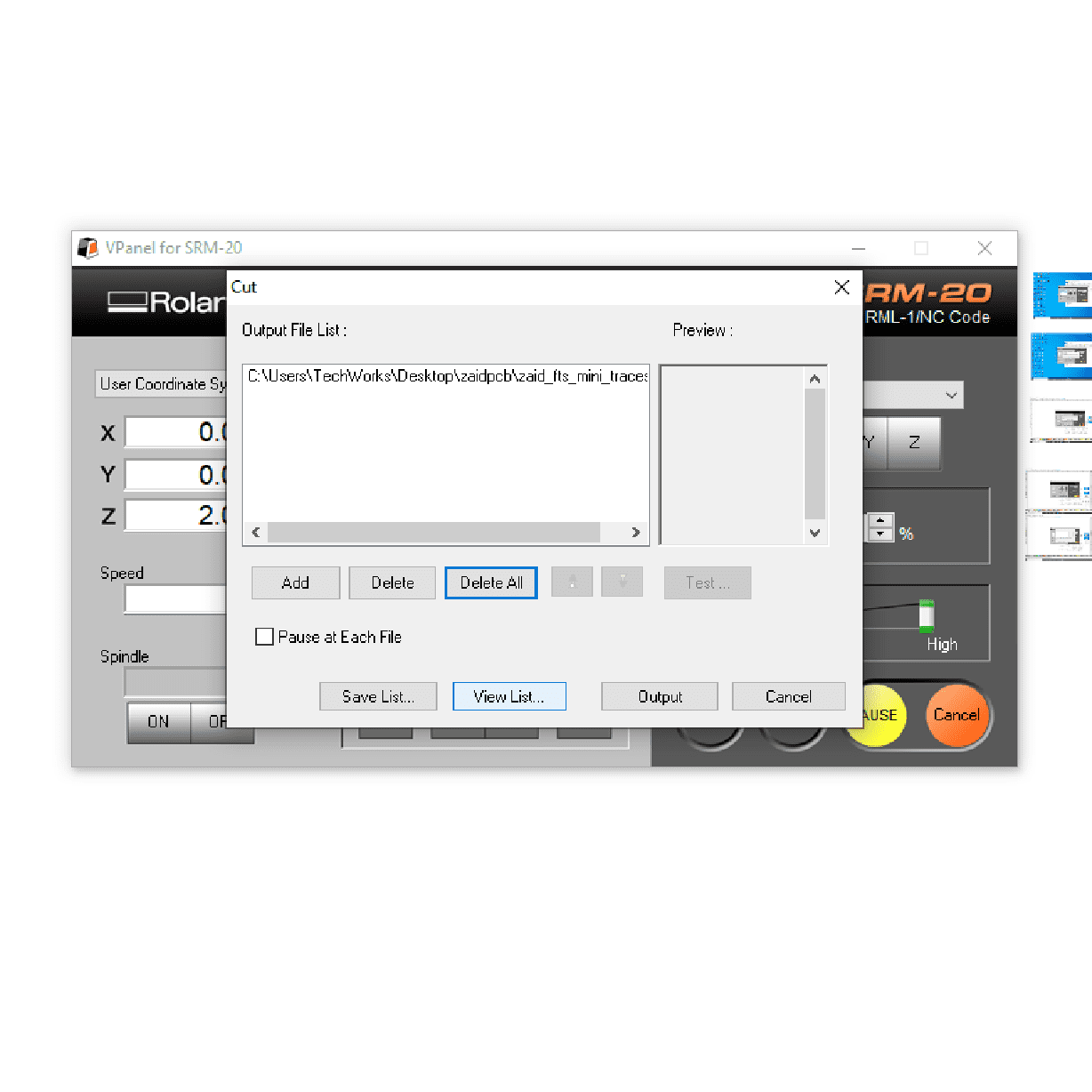
Step 6: Click on “Cut” and click on “Delete All” to remove any old jobs. Click on “Add” and select the traces rml file. Click on “Output”. The machine should start now.


![]()
![]()
![]()
![]()
Assembling the PCB
List of parts:
| Description | Reference | Quantity |
|---|---|---|
| ATtiny45 | U1 | 1 |
| Resistor 1 kOhm | R1, R6 | 2 |
| Resistor 499 Ohm | R2, R5 | 2 |
| Resistor 49 Ohm | R3, R4 | 2 |
| Zener diode 3.3 V | D1, D2 | 2 |
| Orange LED | D3 | 1 |
| Red LED | D4 | 1 |
| Capacitor 100 nF | ISP | 1 |


![]()
![]()
Check Your Work
While it may seem early to start debugging already (we haven’t even tried anything yet!) it is always prudent to check your work before plugging in a board. It only takes a couple of minutes and can save you headaches down the road.
Check your board against the schematic and PCB layout image to make sure that you have installed the correct components in the correct locations and orientations. Inspect your board visually. Components should be flat on the board, not tilted with pins in the air. Solder connections should be smooth, and solder should have flowed both onto the pin and onto the pad. If you still see a lot of exposed copper on the pad, or the solder is lumpy and draws up into a point where you removed the iron, you probably don’t have a good connection. Reflow by applying heat and flux (either from a flux pen or by adding a tiny bit more solder). Also look for unwanted solder bridges between nearby traces and pins. Use a multimeter to check for shorts between VCC and GND.
Reference 2: Building the FabTinyISP
![]()
![]()
Software Installation


![]()
Get and Build the Firmware
Download the firmware source code and extract the zip file (on Linux, unzip fts_firmware_bdm_v1.zip). Open your terminal program and cd into the source code directory.
Run make. This will build the hex file that will get programmed onto the ATtiny45. When the command completes, you should now have a file called fts_firmware.hex. If the command doesn’t complete successfully, something is wrong with your toolchain installation. Consult the error messages for information that will help you debug it.


![]()
![]()
Program the ATtiny45
The programmer and the FabTiny ISP target board are supplied from the PC USB port. Make sure that jumpers are bridged in both to power the boards. Now we are ready to use the programmer to program the new FabTiny ISP.
Step 1: Download “Firmware Source Code” ZIP file and extract it. Run “Git Bash” inside the folder “fts_firmware_bdm_v1”.
Step 2: In “Git Bash” command window run “make”. This will generate “fts_firmware.hex” file, which will be programmed to the target FabTiny ISP. Note that the default programmer defined in “Makefile” is the “usbtiny”. You can check that by opening the “Makefile” and look for “PROGRAMMER ?= usbtiny”. If you are using another programmer you have to change here (use Notepad++).


 sudo make clean : Deletes existing executable files in the directory.
sudo make hex : Creates new updated files.
sudo make clean : Deletes existing executable files in the directory.
sudo make hex : Creates new updated files.
Then I opened the MakeFile and commented this line AVRDUDE = avrdude -c avrisp2 -P usb -p $(DEVICE) by adding a hashtag “#” and instead I typed AVRDUDE = avrdude -c stk500v1 -P /dev/ttyACM0 -b19200 -p $(DEVICE)


![])
![]()
![]()
Test the USB Functionality

![]()
I want to make sure that the USB on your my works,
before blowing the fuse that will enable it as a programmer.
step 1 :Unplug your board from the USB port and disconnect the programmer
step 2 plug it back in to the USB.
step 3 Make sure the programmer you used to program your board is also disconnected from the computer.
we used Linux so I printed “Type lsusb” in the terminal, which will list USB devices.
If you see a “Multiple Vendors USBtiny” device, it worked!
If it didn’t, the dmesg command might provide more info on what went wrong. You want to see a message about a “New low-speed USB device” without any further errors. (Note that sudo dmesg -c will clear the messages after printing them out, which is useful to do before plugging in your board so you’ll be able to tell exactly which messages are a result of plugging it in). If you don’t see the “new low-speed device” message, check the pull-up on the USB line (the 1kΩ and 499Ω resistors, R1 and R2, in series between VCC and D-) for correct values and good connectiions (the computer uses these resistors and their values to detect what type of USB device has been connected). If you do see the “new low-speed device” message, but there are other errors after, try the following:
Sometimes it’s just a bad connection with the port; try unplugging and replugging. Check to make sure that the USB contacts are clean, and have even amounts of solder on all of them, and that the surfaces are smooth. USB 2.0 ports are more likely to work than USB 3.0 ports. If you don’t have any USB 2.0 ports, try plugging in through a USB 2.0 hub. Check the traces and components between the USB data pins and the microcontroller. Make sure the zener diodes are in the correct orientation, that the series termination resistors (R3 and R4) are the correct values (49Ω) and that the connections are good. Measure continuity between the resistors and the USB contacts, and the resistors and the microcontroller pins that they connect to (pins 2 and 3). Check for shorts between microcontroller pins 2 and 3, and to other nearby traces. Try plugging into a computer that you know has worked with someone else’s board, or try plugging someone else’s known working board into your computer. This will help you narrow down whether you have an incompatibility with your USB ports or a problem with your board.
![]()
Blow the Reset Fuse
The ATtiny45 on the board has the code loaded onto it and is working correctly if you’ve made it this far. There are two final steps left to turn your board into a programmer that can program other boards.
First, we need to change the bit that will turn the ATtiny45’s reset pin into a GPIO pin. Once again, this will disable our ability to reprogram this ATtiny45 in the future, which is why we wanted to make sure everything was working before doing this. Connect your ISP programmer to your board one more time, and run make rstdisbl. This does the same thing as the make fuses command, but this time it’s going to include that reset disable bit as well. You should see some progress bars, and with that, avrdude will never be able to talk to this chip again through the ISP header.
Second, we need to disconnect VCC from the Vprog pin on the ISP header by removing the bridge on the solder jumper. Sometimes the excess solder will stick to a clean soldering iron tip; if not, use desoldering braid to remove the solder from the jumper, thus breaking the connection.
Reference 2: Building the FabTinyISP


![]()
![]()
Test Your Programmer
You should now have your very own working ISP programmer! But, before I used my board to try programming another board which is my friend Amma’s board .
with make flash


![]()
![]()
Code
![]()
download files
![]()
