Electronics Design
Test Equipment
The pandemy has caused that FabLab Puebla closes its doors. Thus, I was not able to go there. Fortunately, I studied Mechatronics engineering and I learned how to use multiple equipments such as oscilloscope, miltimeter, signal generator, and many others. At my place, I only have a multimeter because the other equipments are expensive and I am not able to afford them. My multimeter has the following specifications:
- Precision: 5 digits
- Maximum input voltage: 600V CAT III
- Fuses: FF 250mA H 600V and FF 10A H 600V
- Negative polarity: Yes
- Working temperature: 0° C to 40° C
- Others: It can measure voltage, current, resistance, continuity and diodes
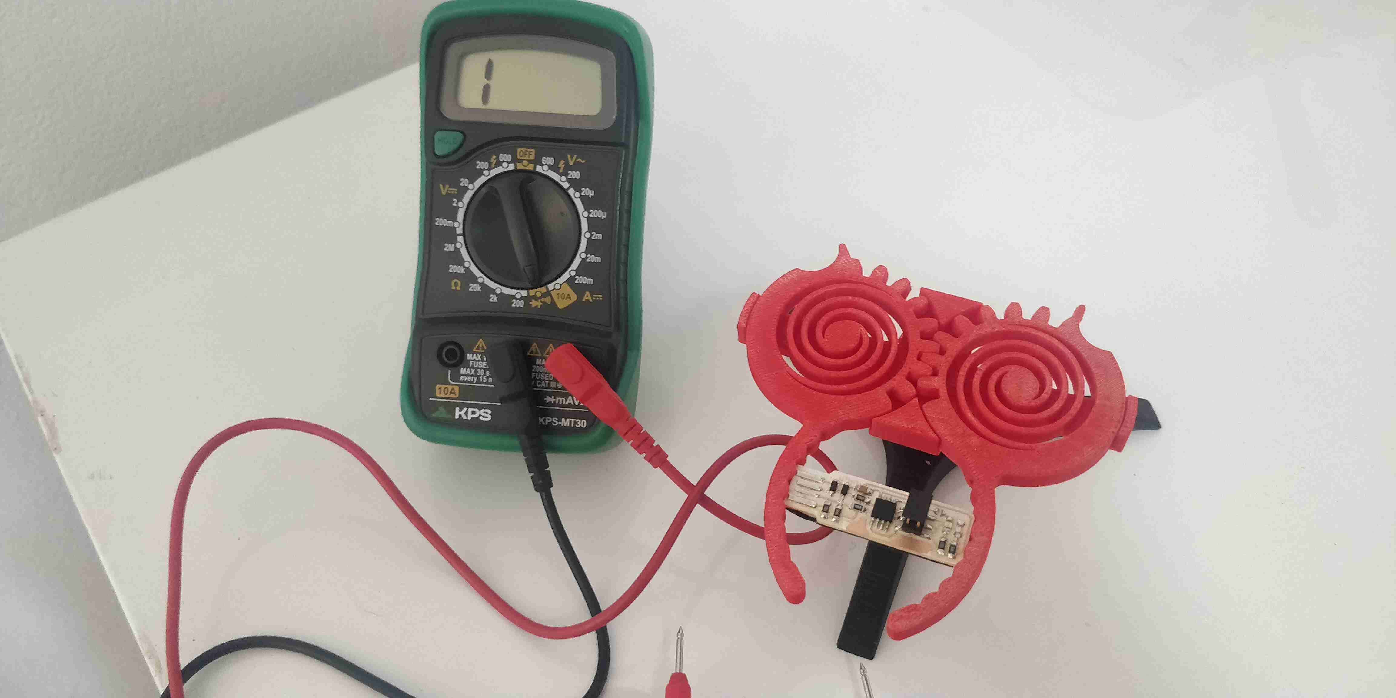
I tested multiple functions of the multimeter and the most important is how to use the probes because depending on the measurement, you must place the probes in parallel or serial with respect to the desired component to be measure. Also they are three connector where the probes can be placed the on in the middle or COM must have always the black probe while the other two use the red probe depending on the desired measurement.
| Measurement | Symbol | Red probe |
|---|---|---|
| DC Voltage | Right connector | |
| AC Voltage | Right connector | |
| DC Current | Right connector >200mA Left connector <200mA |
|
| Resistance | Right connector | |
| Continuity/Diodes | Right connector |
Main Board Axolbot
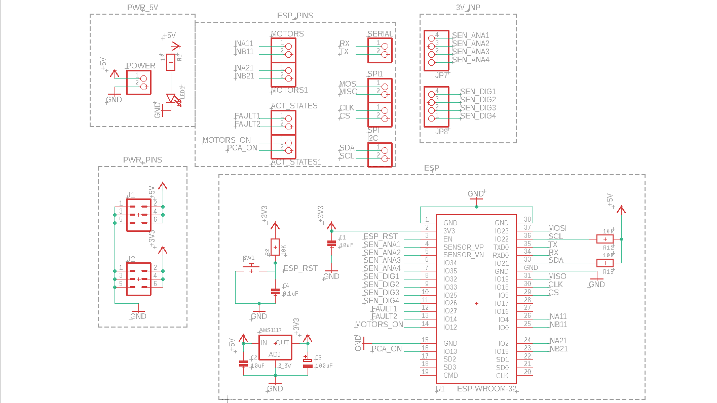
I want to create a robot for my final project and one of its particularities is that he can control multiple servomotors and motors via I2C but it can also handle digital and analog sensor. Therefore, I decided to create a board powered by a ESP32 because it has WiFi and Bluetooth connectivity. The board must have pins for the I2C, Serial and ISP protocol as well as multiple power pins to provide 3.3 or 5V. But first, I analized a board that contains a ESP32 and show the pinout of the board but most important, it shows the capabilities of each pin.
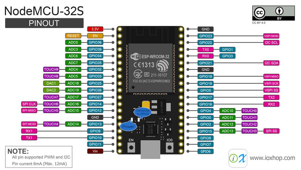
With this pinout, I assigned the task of each pin according to my requirements. These description is shown below:
| GPIO | Pin name | Description |
|---|---|---|
| 23 | MOSI | ISP protocol |
| 22 | SCL | I2C protocol |
| 1 | Tx | Serial protocol |
| 3 | Rx | Serial Protocol |
| 21 | SDA | I2C protocol |
| 19 | MISO | SPI protocol |
| 18 | CLK | SPI protocol |
| 5 | CS | SPI protocol |
| 4 | INA11 | Enable motor 1 |
| 0 | INB11 | Enable motor 2 |
| 2 | INA21 | Enable motor 3 |
| 15 | INB21 | Enable motor 4 |
| 13 | PCA_ON | Enable PCA9685 |
| 12 | MOTORS_ON | Enable H-bridges |
| 14 | FAULT2 | H-bridge 1 state |
| 27 | FAULT1 | H-bridge 2 state |
| 26 | SEN_DIG4 | Digital sensor at 3.3V |
| 25 | SEN_DIG3 | Digital sensor at 3.3V |
| 33 | SEN_DIG2 | Digital sensor at 5V |
| 32 | SEN_DIG1 | Digital sensor at 5V |
| 35 | SEN_ANA4 | Analog sensor 4 |
| 34 | SEN_ANA3 | Analog sensor 3 |
| 36 | SEN_ANA2 | Analog sensor 2 |
| 39 | SEN_ANA1 | Analog sensor 1 |
Designing the board
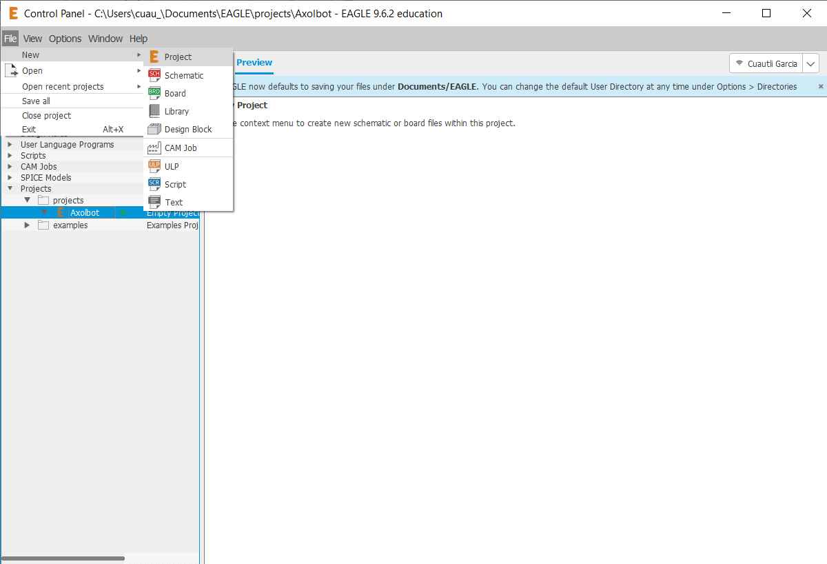
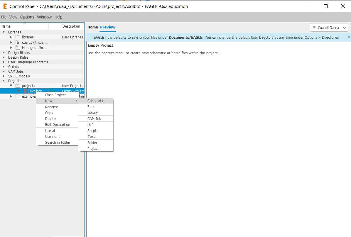
Once I was able to define all the possible inputs/outputs that my robot needs. I proceed to create the schematics of the board in Eagle. But first, I had to create a project with the following option clicked on File -> New -> Project. Later, I create a schematic with right click on the created project -> New -> Schematic. Thes procedures are shown in the following pictures.
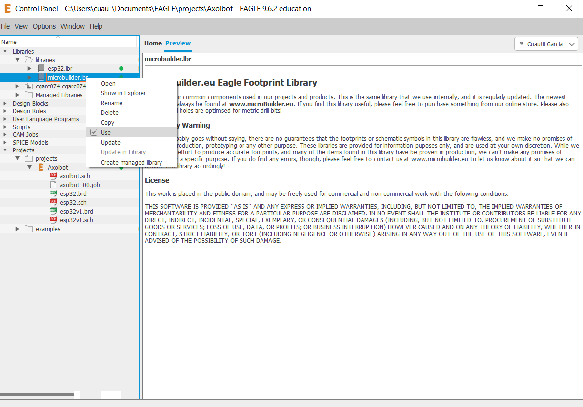
Now, it is time to place the components and created my first schematics. Nevertheless, when I looked for the ESP32 I was not able to found it. Therefore, I searched a library that contains this component and I found out that it has the DRV9685 and the DRV8833 which I will use in the future (The library is called microbuilder). To install it, I copied the file into the library folder that is show under Options->Directories. After the file was copied in the same folder, you need to go to the Control Panel and under libraries you must see the microbuilder library. If you can see it, you just have to righ click on the library and click on "use" as shown in the image below.
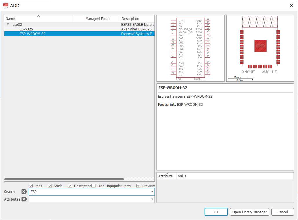
The next picture shows how the component appers when we search for the ESP32 in the add tool
Thus, I created the schematics based on the pin declaration of the previous table and I also used the schematics of a ESP32 for guidance about places where I can put my components. The created design contemplates a reset button, a LED that tells if the power is connected, multiple connector for the communication protocols and the voltages as well as two level convertes for the digital sensor that work with 3.3V.
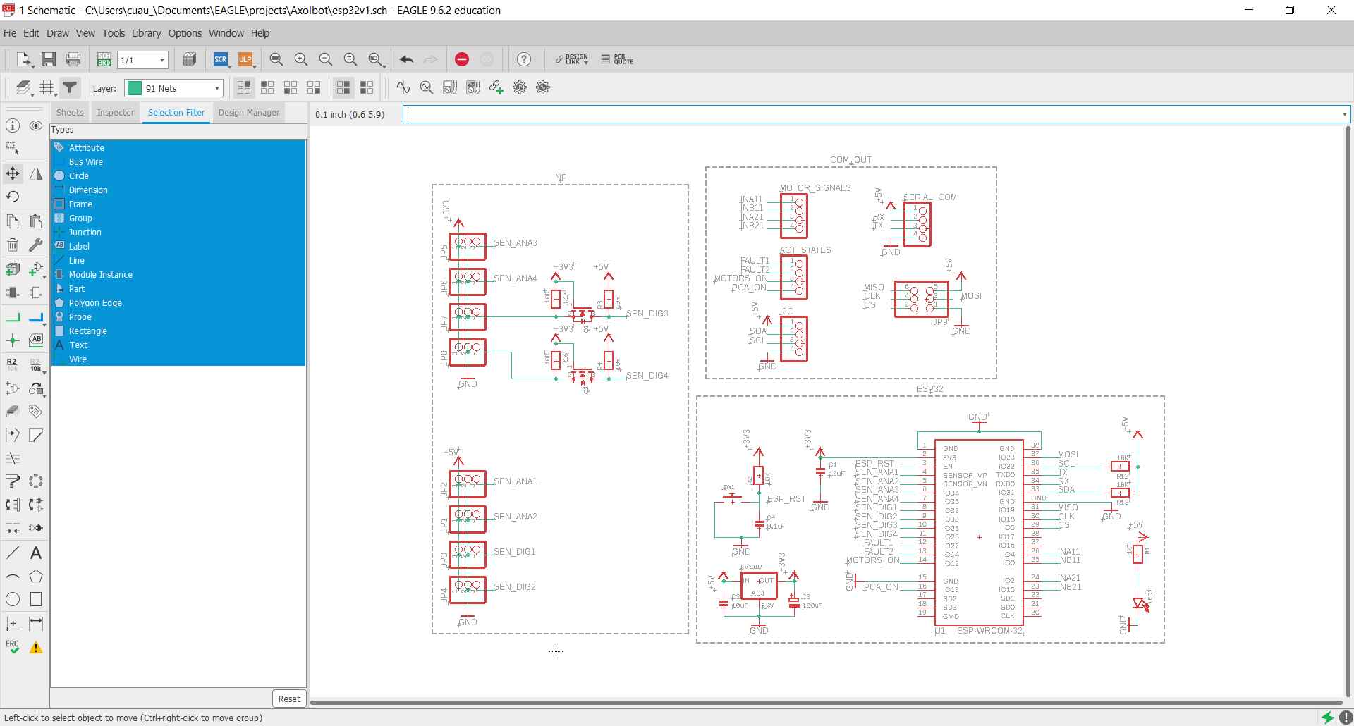
As you can see, I did not wire up everything but instead I use the name function on the left bar to change the name and creae labels. This procedure makes a clean schematics and it is also easier to comprehend. Another option that I used was the block option because the circuit is a little bit big and it is easier to separate the main task of the components and put togheter the ones that perfom the same task. To create the block, you can use the selection tool on the left side, select the components, and right clik to select New Group where you just need to give a name to it and that is all.
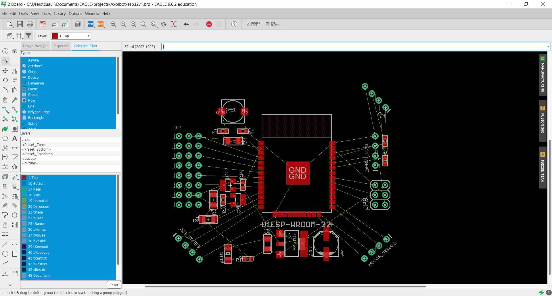
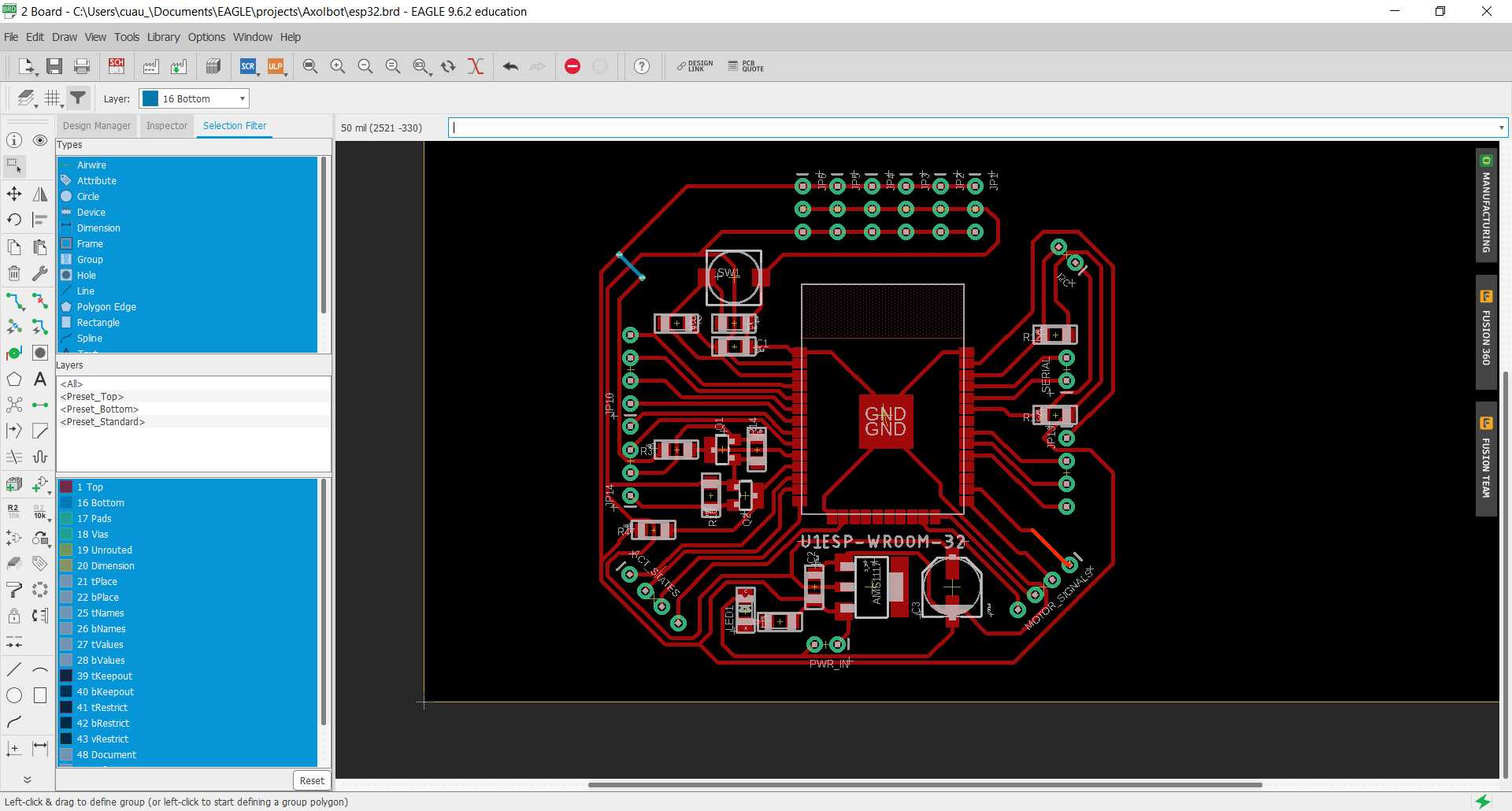
Once I finished the schematics, I moved to the board section to place the components and create the required paths. To open the board section, you just need to click on the the button called SCH/BRD that is next to the printer button. After the components were shown, I move them in such a way that I imagined. First, I move the ESP32 because it is the main board and later all the other components in a place next to the input/output signal of the microcontroller. The next figure shows the first attempt to arrange the components.
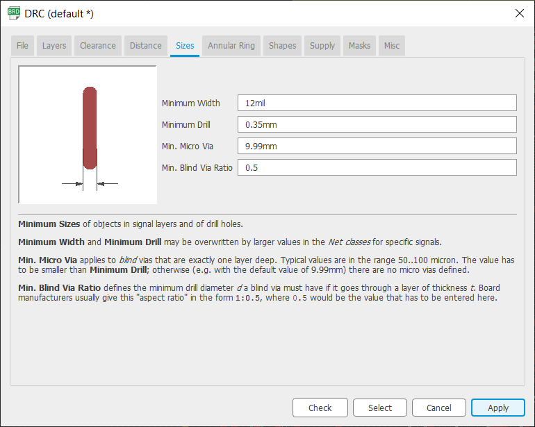
Now is time to declare the design rules, so we can verify that the proposed layout of our board will be correctly machined and that there will be no problem. To chane these setting, you must go to tools->DRC. In my case I use 16 mil or 12 mil depending on the fields because the ESP32 pads are really small and I have multiple components. The following pictures show my design rules.
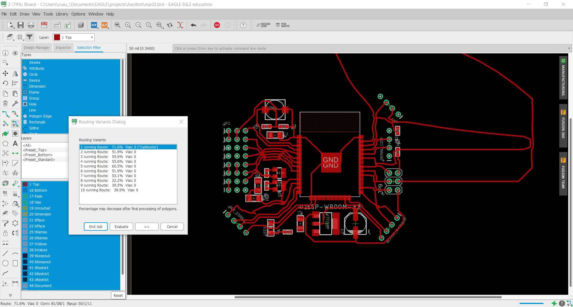
Since my design is a little complex, I decide to use the autoroute option to see how the paths will be generated and if if would be possible to do it in one layer. The autoroute option is on the left menu that resembles a path with a lighting bolt. When you click on this icon, a new window will be displayed and there you just need to change the bottom layer by N/A because we want a board with a single layer. Later, I changed the effort to medium and I clicked continue. The software will generate multiple options to get the most optimal paths, the next picture show the the middle of the autoroute progress.
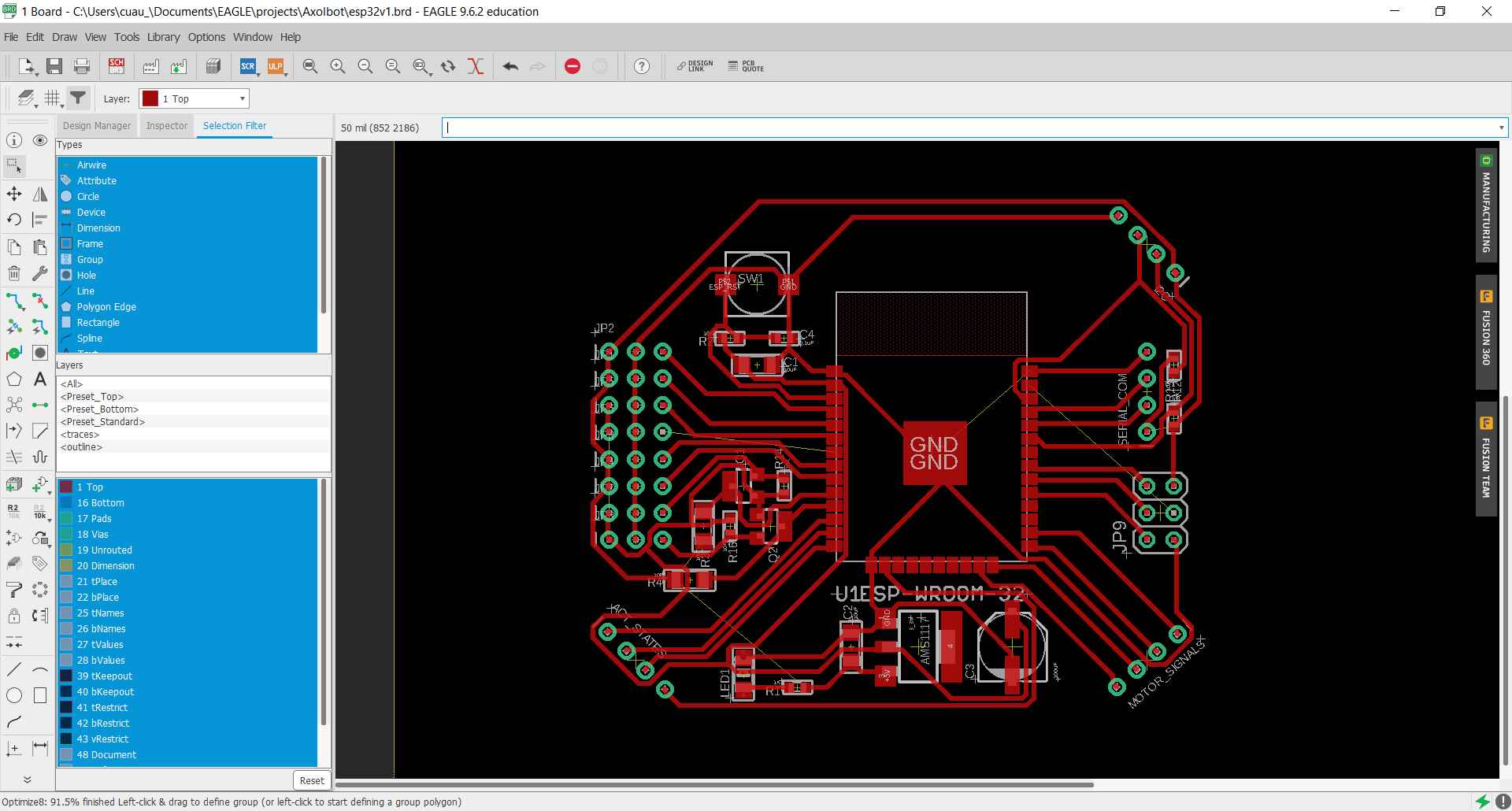
The following figure shows the final result of the autoroute process. However, I found out that there were many unconnected paths and I tried to change them manually to find a better way to place them.
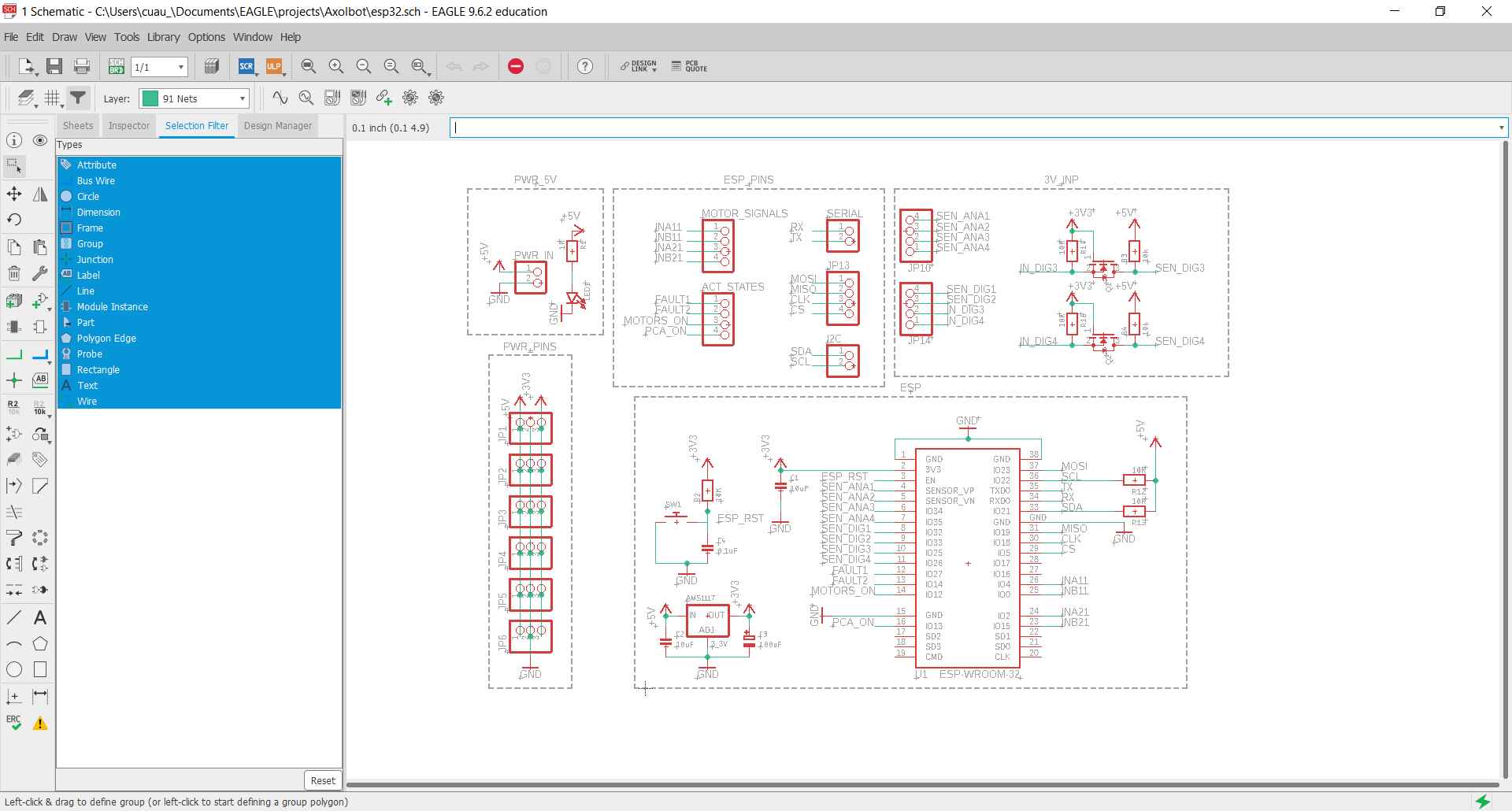
After many hours, I realized that there were no way to connect all the paths in a single layer so I decided to change the schematics and instead of having power and GND in the same pin header as the sensor or the communication protocols, I created another pins that have 5V, GND, and 3.3V in case that the user needs them. Thus, the new schematics looks like this:
With the new schematics, I did the routing manually since I already knew the possible paths that the pincs could have. Furthermore, it was really helpful because I was able to move some of the items for a better location. Then, I succed to have almost all the components in a single layer with the exception of 5V. I had to create a via to join two paths of 5V because I did not find another way to do it. To create a via, you just need to click on the green circle with a blue and red line to place a via in the path where you desire. After you created your vias you need to change to the bottom layer and join the vias. It is important to note that this new path will be blue.
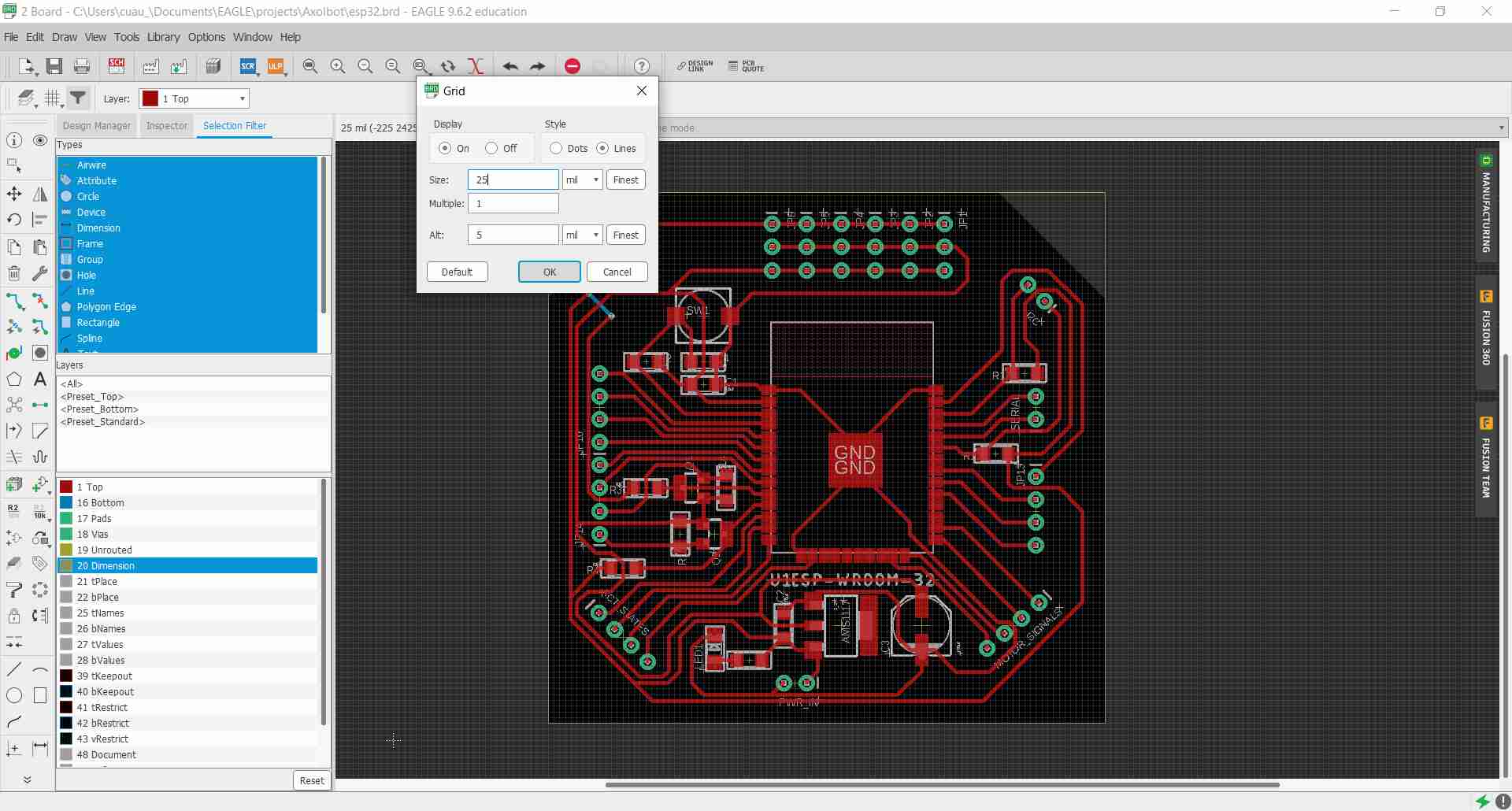
With my final design done, I activate the grid to create an outline. The grid was activated because it is easier to move and allocate the outline path with the grid. The grid option is next to the layer settings and it is called grid, I chose a size of 25 and the other options I left them as default. The next picture show the selected options and its results.
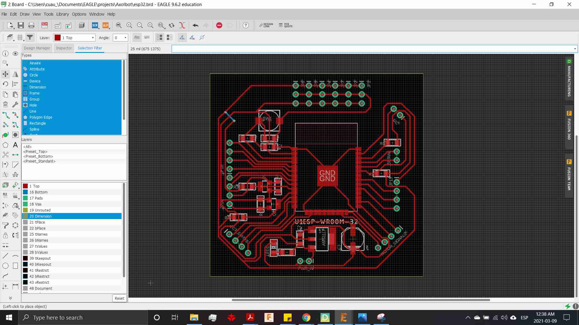
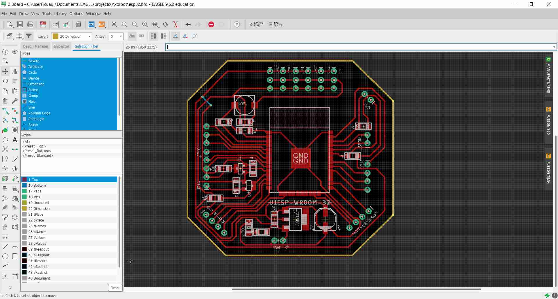
Now to create the outline, I change to the dimension layer and I moved the yellow lines that limit the board dimensions. When I cropped them into a square, I create a new line with around the same square to later use the mitter tool and create a chamfer in the corner as can be seen in the pictures.
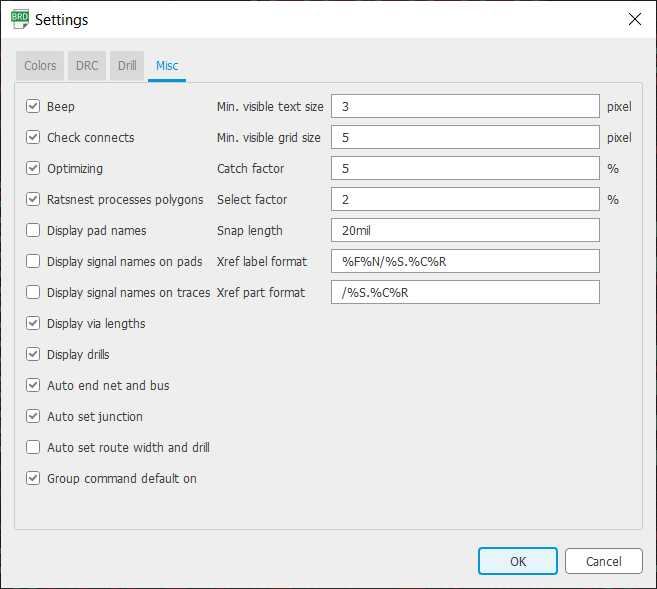
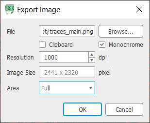
When I finished the dimension line, I wanted to create the monochromatic pictures with the traces and the outline. However, I changed a few setting to erase the paths name because even that is not part of a layer. To do that, I click on Option->Set...->Misc and deactivate the options shown in the first following image. To create the PNG images, I clicked on File->Export->image and changed the dpi's to 1000, activated the monochromatic option and selected the file name ans its folder.
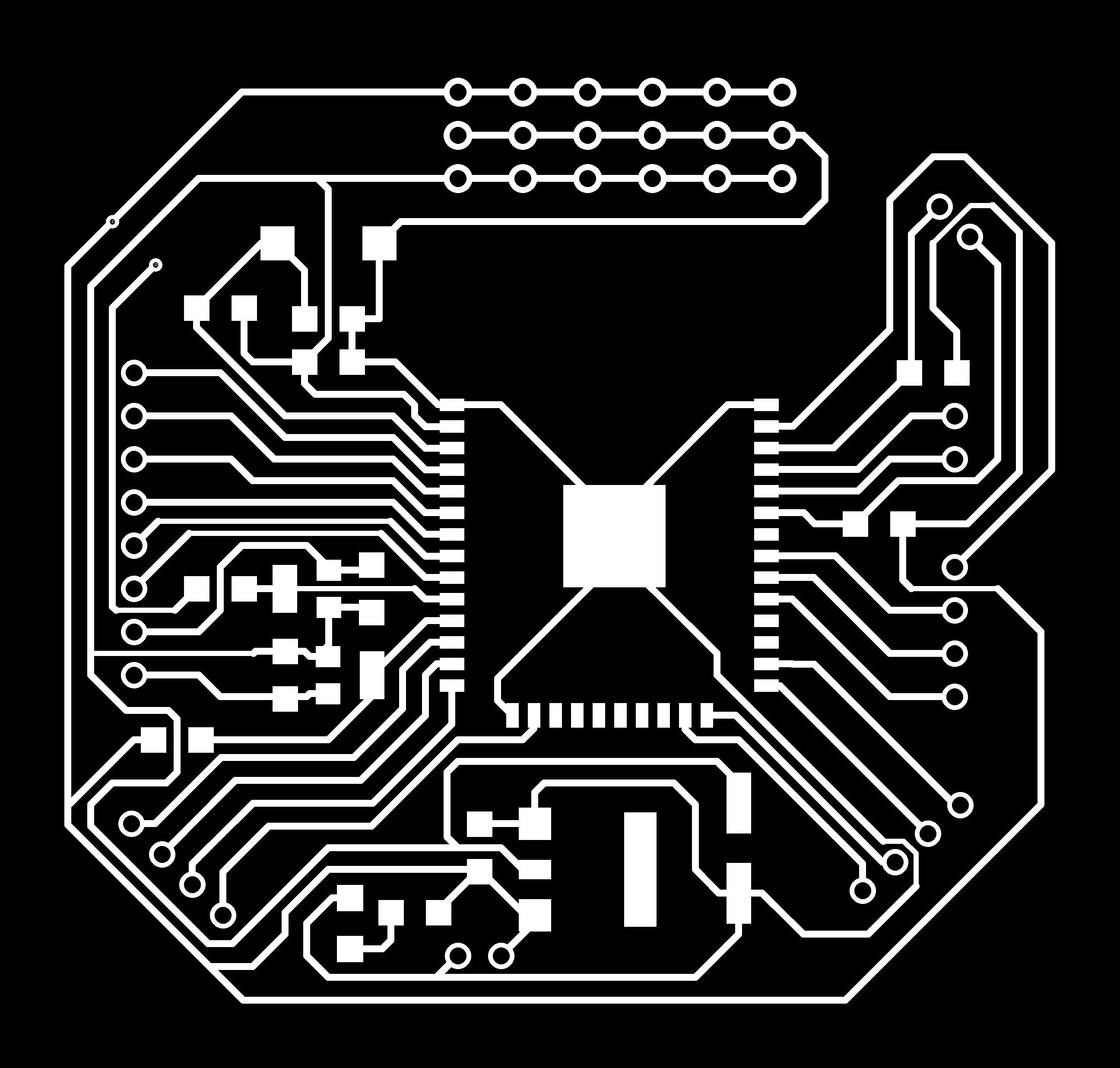
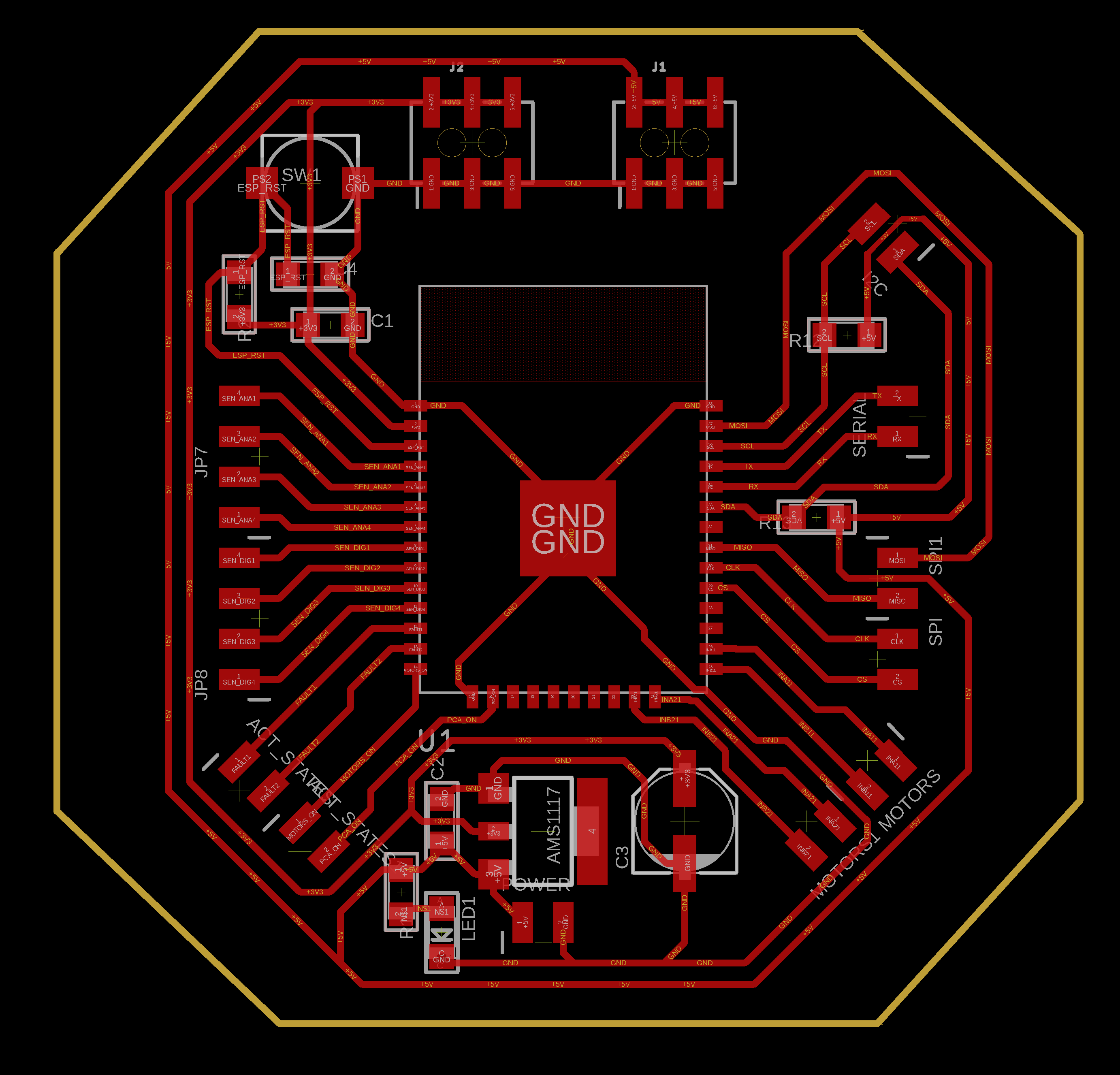
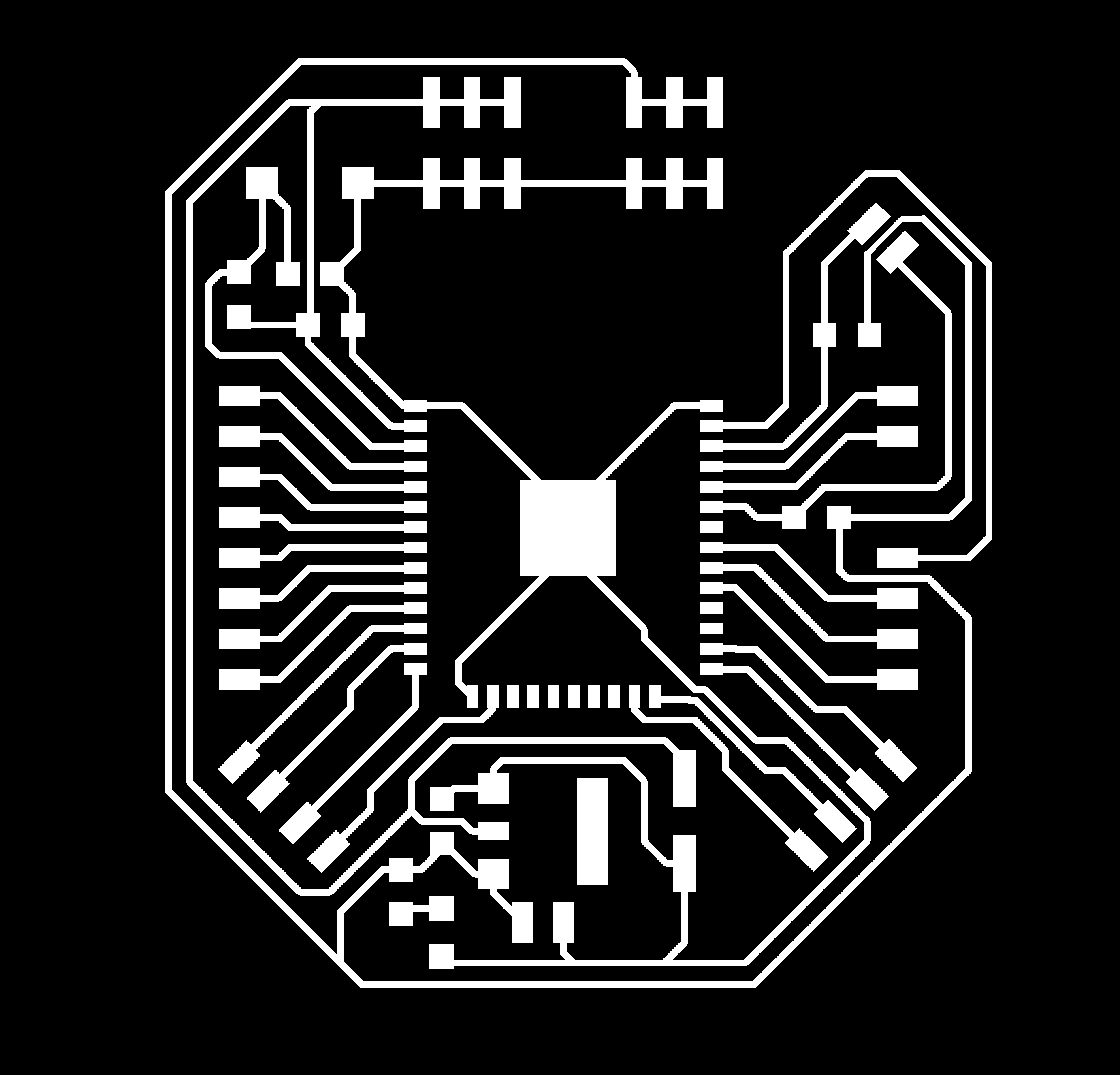
Before creating the png images, I change the visibility of the layers that I wanted for the traces and for the outline. To hide or display the layer, you can go to View->Layer Setting and click on the eye next to the layer to hide or click on the left side of the layer name to display it. Thus, my final images with the traces and outline are shown below:

Machining the board
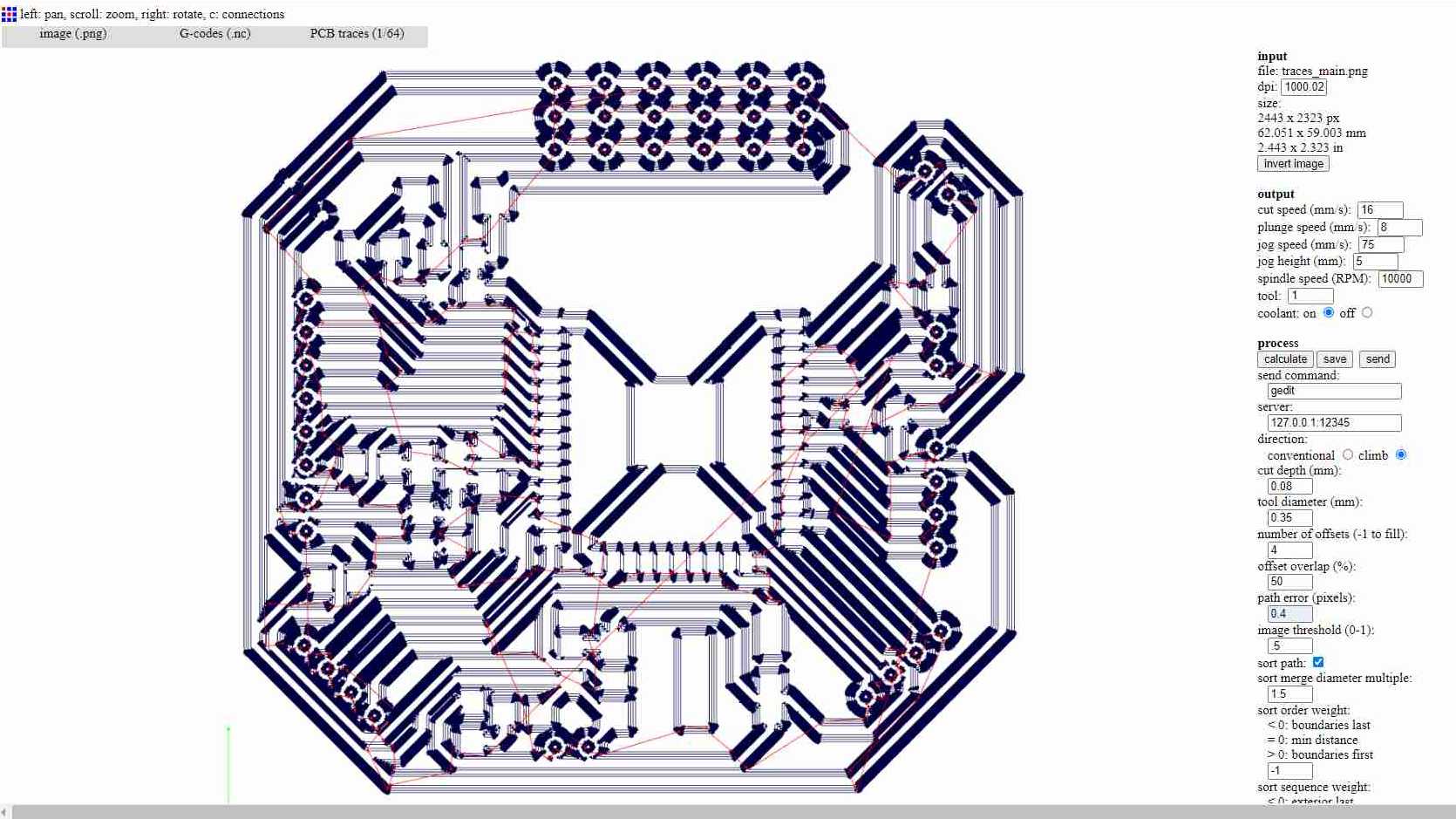
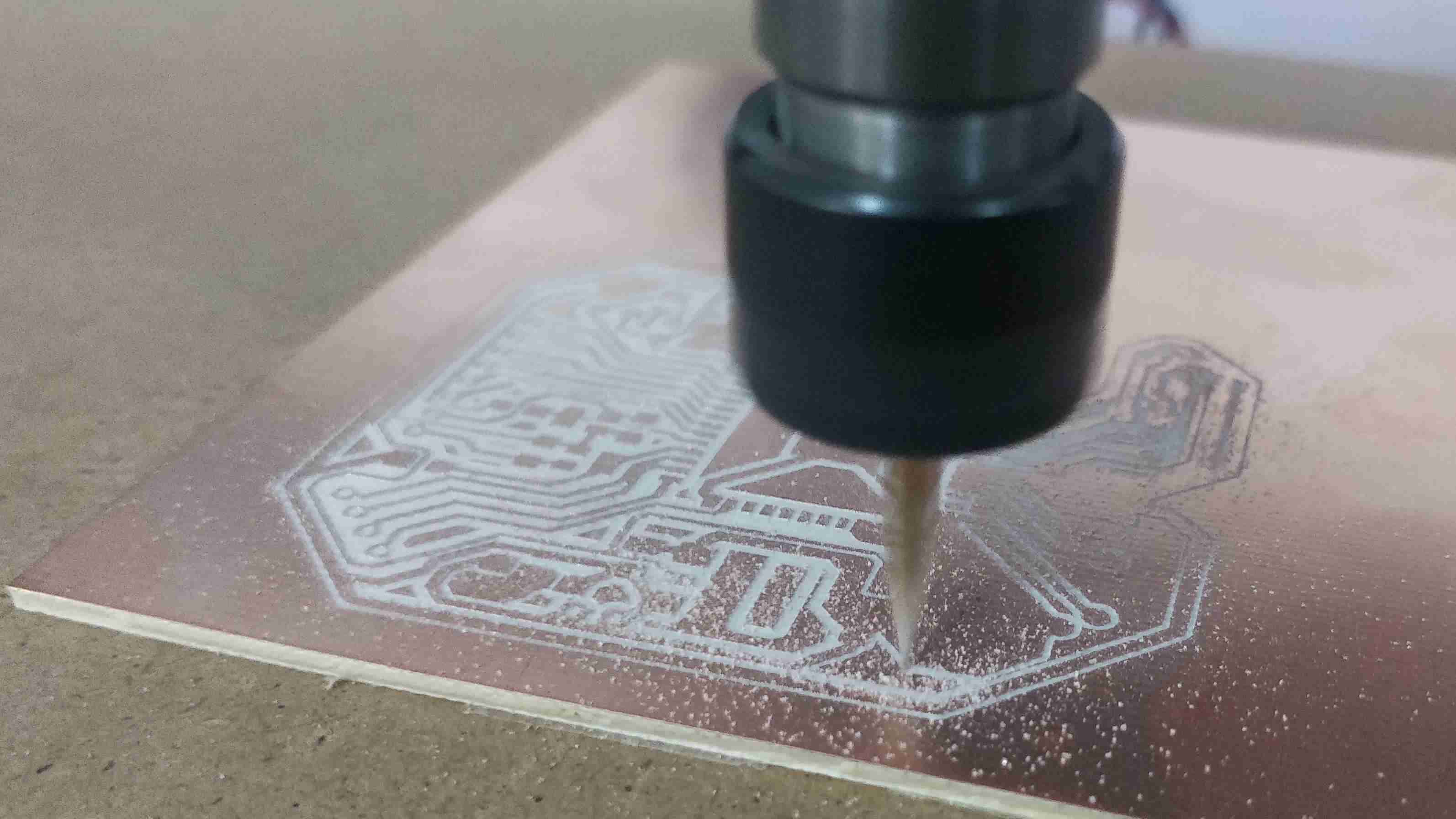
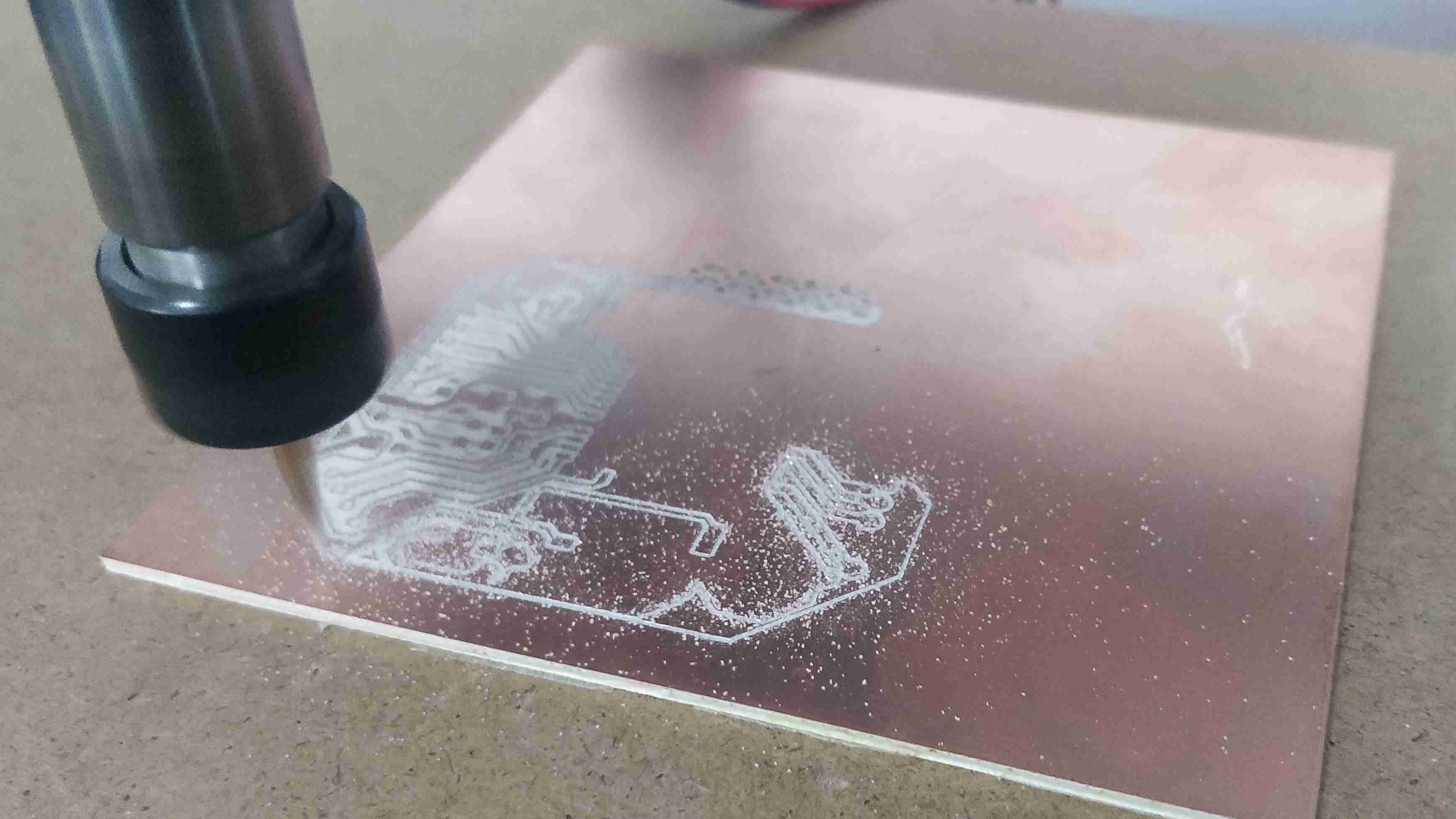
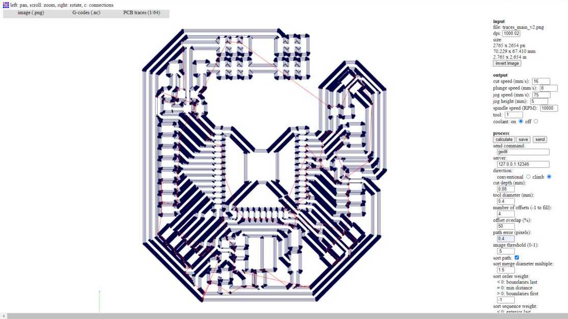
With the images to machine the PCB, I use fab modules to create the g-code and send it to my CNC mill. Remembering that we must select the image gotten from Eagle in a png format, later we must set the G-code as a output format, then we select PCB traces (1/64) for the traces and PCB outline (1/32) for the outline of the board. And finally we use the same parameters as before, cut speed of 15 mm/s, plunge speed of 8 mm/s, cut depth of 0.08 mm, tool diameter of 0.4 mm and 4 offsets.
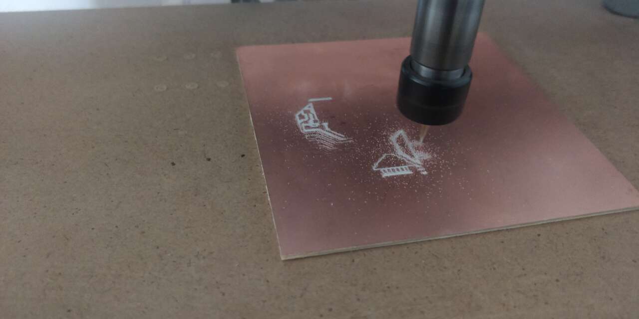
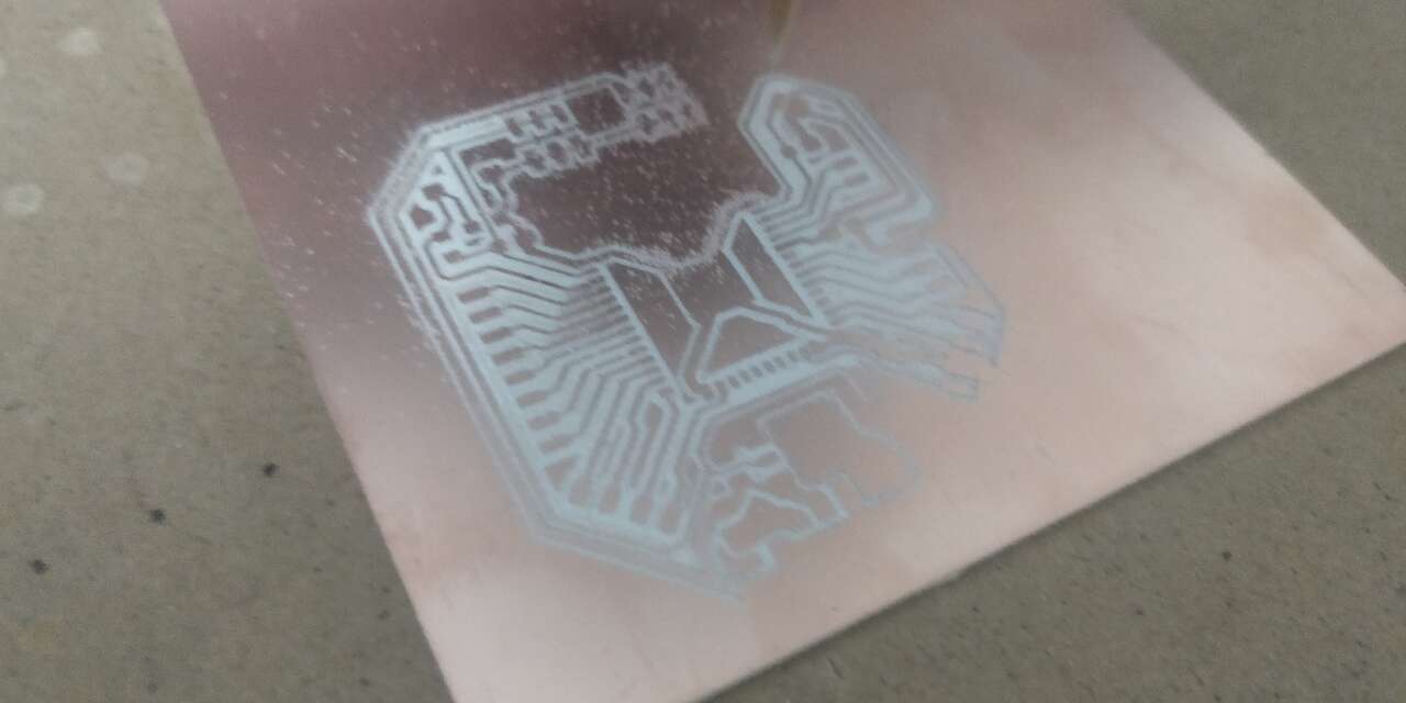
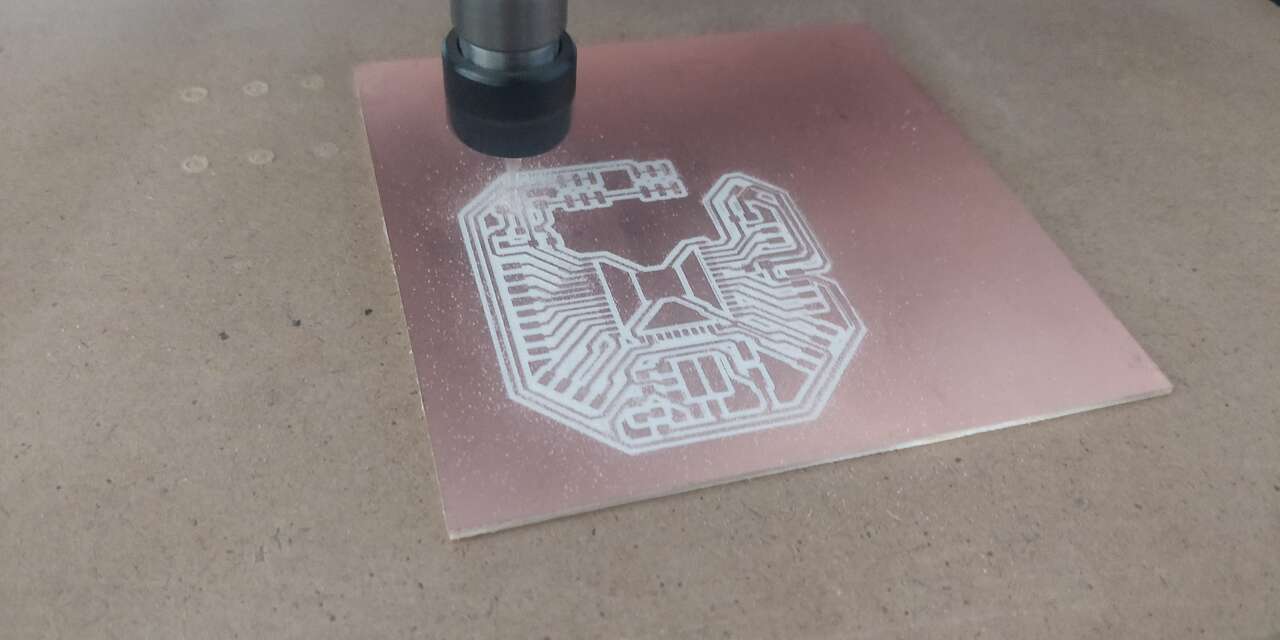
I applied tha same process to manufacture my PCB, where first I placed the PCB over the MDF with double-sided tape and I later set the origin to start the machining process with the G-code generate. The following picture show the machining process.
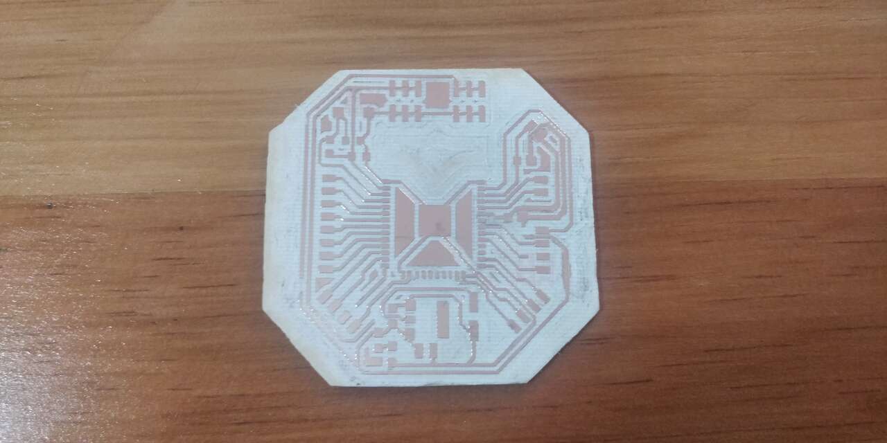
The following table shows the bill of material to create this PCB.
| Quantity | Component | Model | Cost | Total Cost |
|---|---|---|---|---|
| 1 | Microcontroller | ESP32-WROOM | 3.89 | 3.89 |
| 1 | 3.3 Regulator | AMS1117 | 2.02 | 2.02 |
| 2 | Ceramic Capacitor | 10uF | 1.26 | 2.52 |
| 1 | Ceramic Capacitor | 0.1uF | 1.26 | 1.26 |
| 1 | Electrolitic Capacitor | 100uF | 2.33 | 2.33 |
| 2 | Mosfet-N | BS138 | 0.45 | 0.90 |
| 1 | Resistor | 1k Ohm | 0.81 | 0.81 |
| 7 | Resistor | 10k Ohm | 0.81 | 5.67 |
| 1 | LED | 1206 | 0.29 | 0.29 |
| 1 | Push Button | SKPMAME010 | 0.65 | 0.65 |
| 3 | Pin header | 1x2 trough hole | 0.2 | 0.2 |
| 6 | Pin header | 1x3 trough hole | 0.2 | 0.4 |
| 4 | Pin header | 1x4 trough hole | 0.2 | 0.2 |
| 21.14 | ||||
Since FabLab Puebla was not opened for the pandemy, my instructors were not able to send me the required components. Therefore, I will wait a few more days so they can send me the components and in case that it will take more time I will buy the required components in a electronic shop.
Second Version of the board
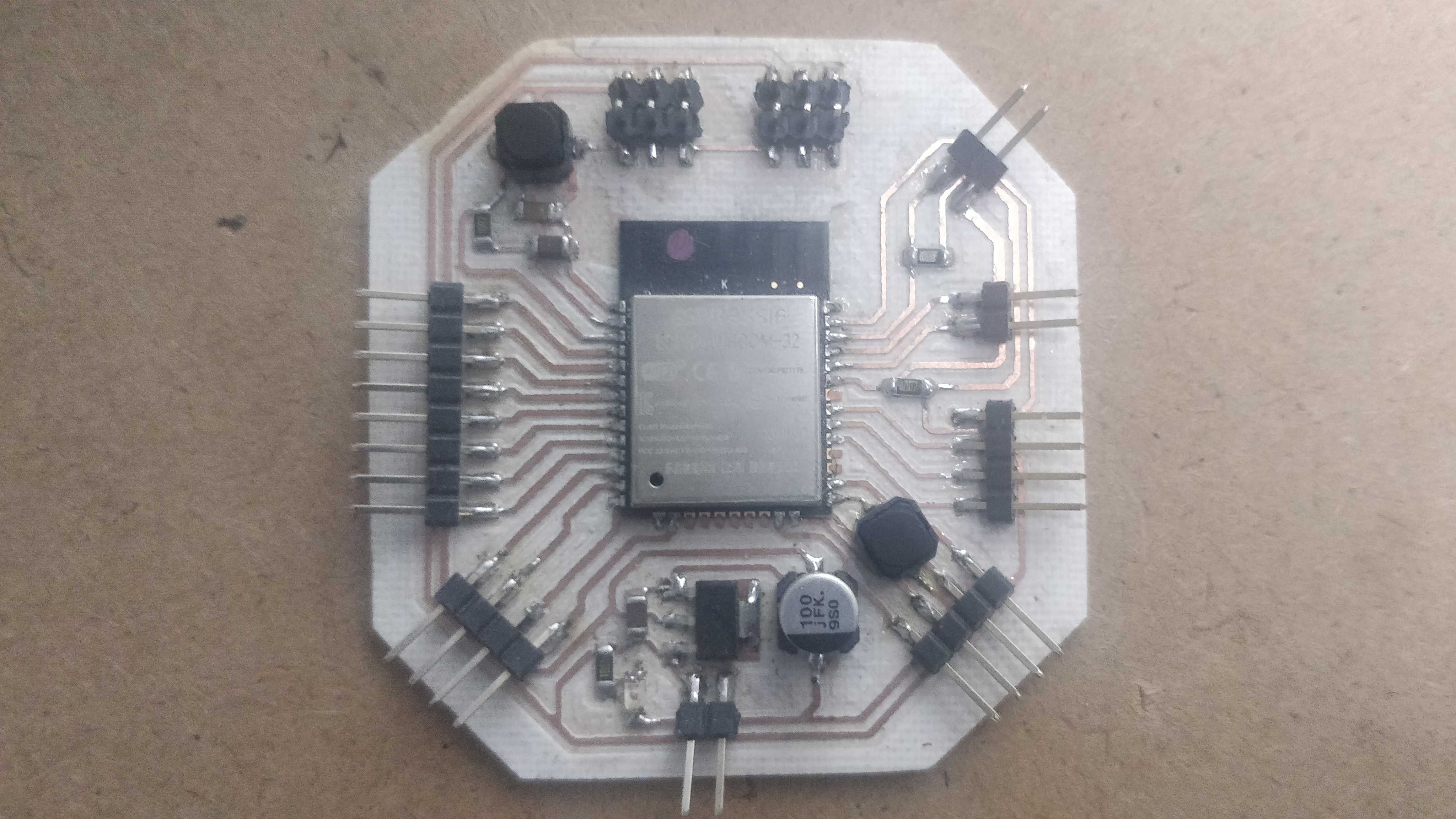
While I was waiting for my board I look for another arranges that I can make with my board to avoid using a double-sided board since in this version I have through-hole pins and I want to use pins that that can be placed in the top layer. Thus, I decided to see any other options to arrange the components and I found out that the board cannot be created with a single layer without erasing the MOSFETs. Then, I erased those two components because they are only used to change teh voltage from 5V to 3.3V or from 3.3V to 5V and they are not really neccesary knowing that the inputs will be restricted to 3.3V
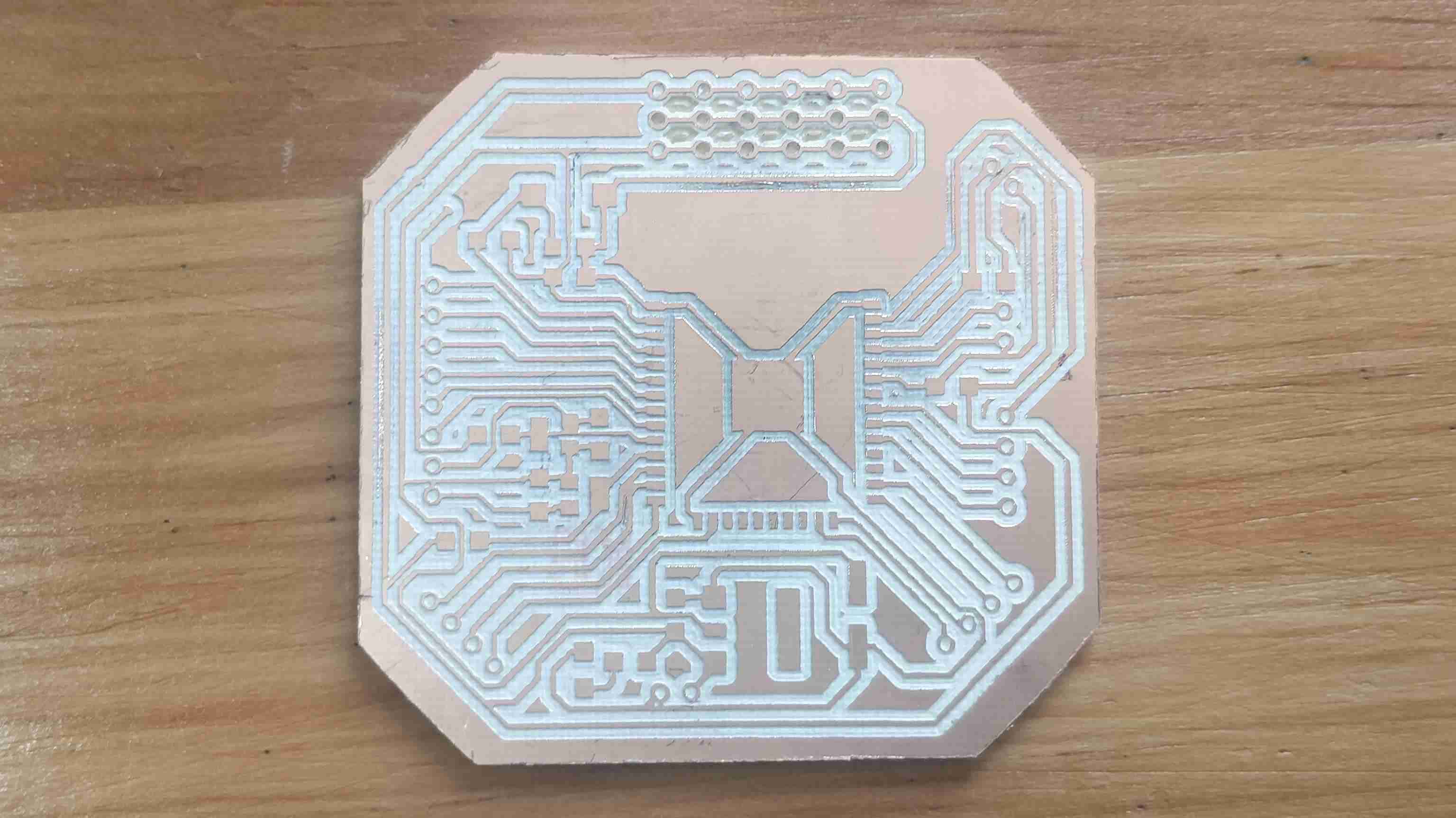
After doing the required changes, I created the new traces and outline files where the most important is that this board is a single layer PCB to ease the fabrication process. The two pictures below show the top layer with the componentes and the traces.
Like the other PCB's, I used fabmodules to generate the G-code and I also used UGS to send the G-code to my Mini Router CNC 3018 PRO.
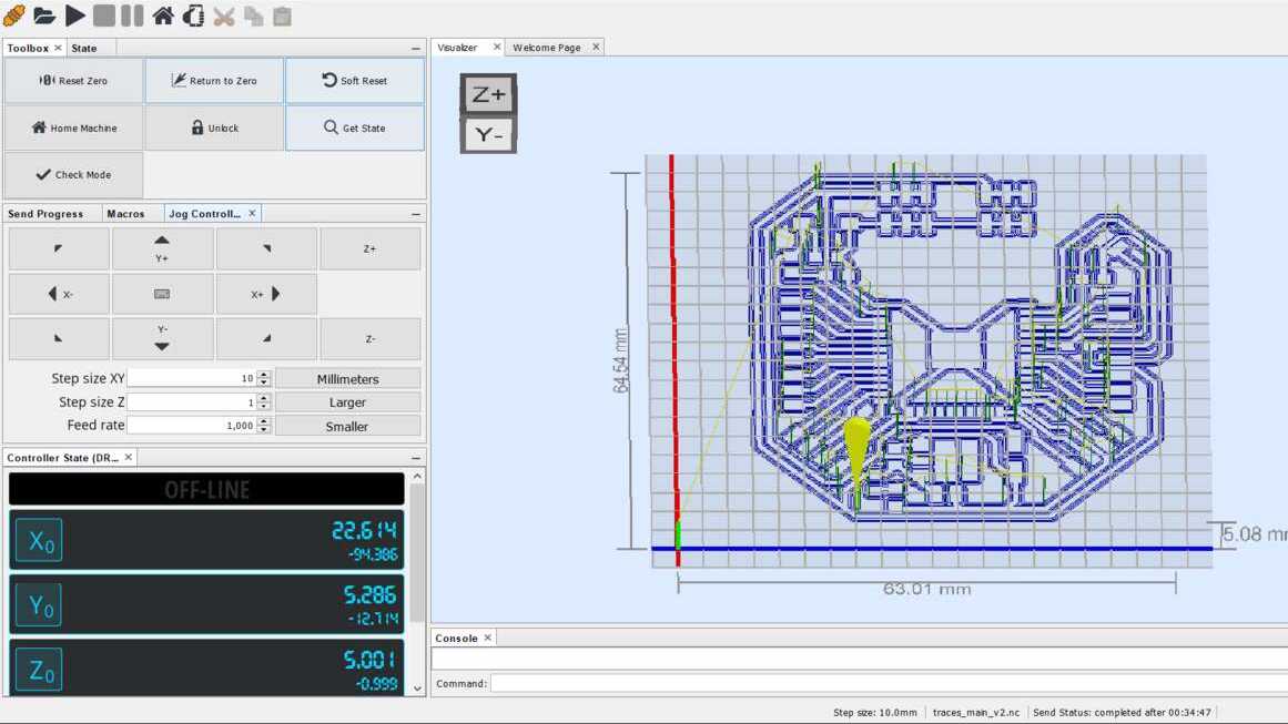
For the machinning process, I make the same setup as before placing double-sided tape in the board, zeroing the machine, uploading the file, and finally sending the file to create it. It is important to note that the pins that I used are not SMD pins but normal pins that I placed almost horizontal to be able to solder and they worked perfectly.
The required components for this board are extactly the same as the previous first version with the difference that the MOSFET are not required and we only need 3 resistors of 10 KOhms. Once I obtained the necessary components, I proceed to solder the componets to the board. Since, I did not know the sensiblity if the ESP32 I decided to solder all the other components first and at make a verification process to see that everything was workind as expected. At the end, I soldered the ESP32 to the board and the final board can be seen below.
Since I was not able to finish the assignment on time due to the late delivery of the electronics. I programmed my board during the Embedded programing week.
Files created
Useful Resources