How to make (almost) anything.
Week 04. Electronics Production
Work done in the Lab under the guidance of my remote Instructor to accomplish the weekly assignments.
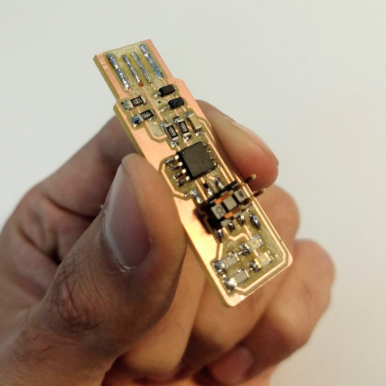
This week I made an in-circuit programmer by milling and stuffing the PCB.
My weekly schedule:
| Wednesday, February 17 | Thursday, February 18 | Friday, February 19 | Saturday, February 20 | Sunday, February 21 | Monday, February 22 | Tuesday, February 23 |
| Global class |
FabISP reading Soldering practice |
Mods test | Regional review | Board milling | Board soldering | Upload documentation |
Group assignment
We characterized the design rules for our PCB production process, you can read it there.

FabTinyISP
My first step for this assignment was to read this webpage, it has a complete description of the FabTinyISP project including PCB fabrication, programming and testing, a lot of new names and concepts that I didn´t fully understand at the time.
It was too much information for my brain so I preferred to try something more practical to clear my mind, so I started practicing welding for the first time. My friend Luis had a lot of damaged boards that I could practice with so I grabbed the soldering iron and started putting drops everywhere.
Mods
Mods includes a lot of useful tools for a FabLab, for this assignment I used Roland SRM-20 PNG program to generate my G-code file. The user guide on PCB fabrication can be found here. All this documentation was for Mods Community Edition, I made a test on the old Mods (linked in the Academy schedule) but I couldn't find any working file export option to cut with an offline machine.
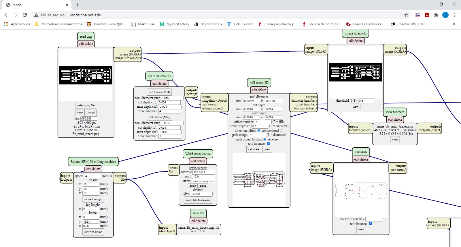
The interface is very intuitive because it uses simple connections of inputs and outputs, so you can see what happens when you make a change in real time.
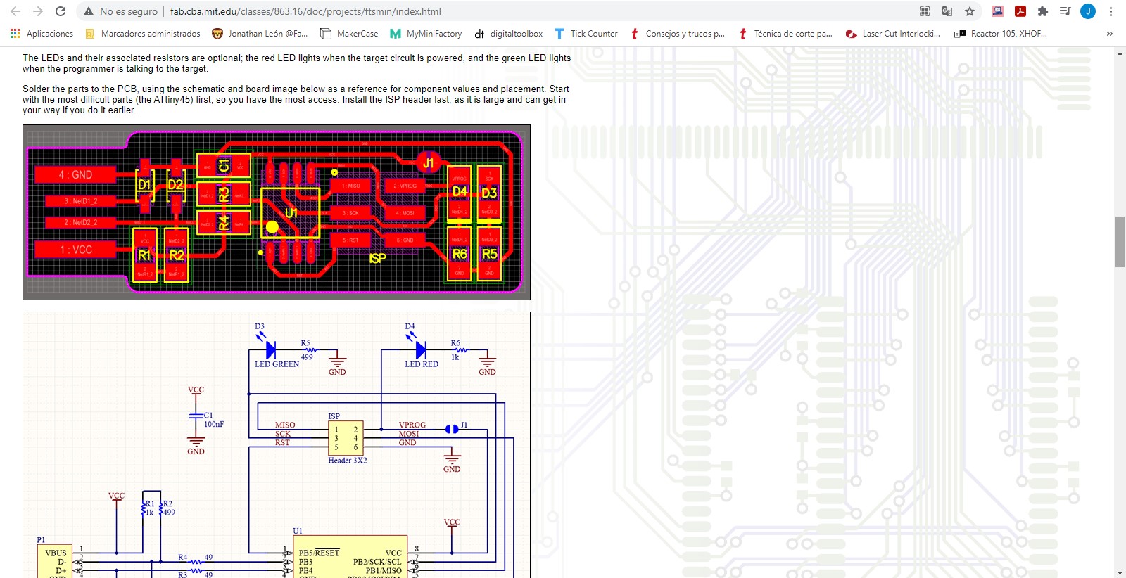
You start uploading your SVG or PNG file, I used the PNG downloaded from the FabTinyISP.
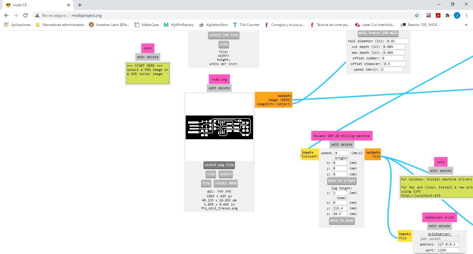
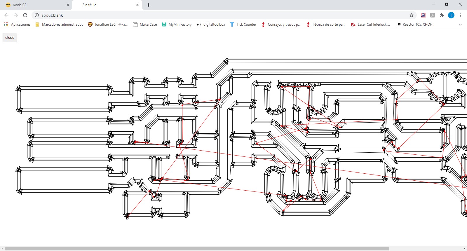
The next step is the tool configuration, you can select one of the default bits or you can enter your own values, then you can calculate the paths and preview them.
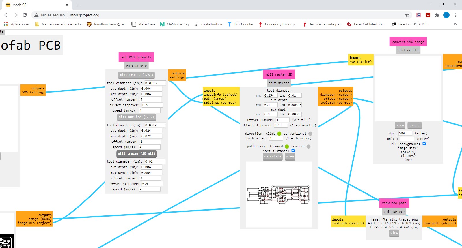
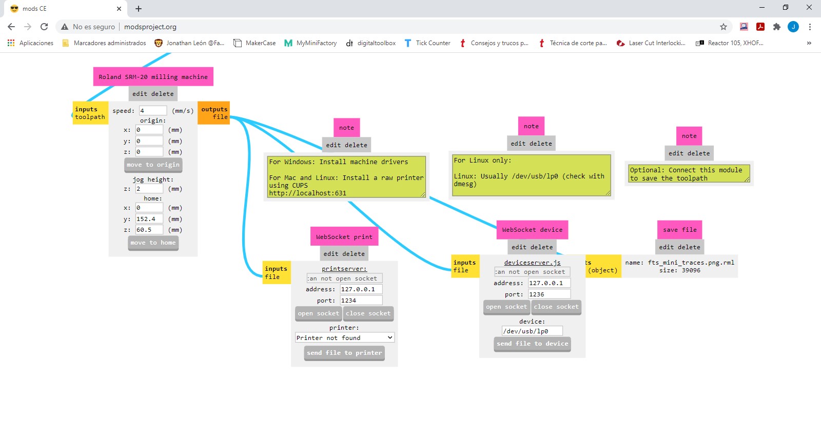
The default speed (4 mm/s) worked great with our machine, the origin should be set on X,Y,Z=0 and the jog height at least on 2 mm for security of the bit and the final piece. When you connect the last module (“Save file”) you can download the .RML file ready to cut on your Roland, I guess you can cut directly from Mods if your machine is connected via LAN (but ours was not).
Roland SRM-20
To send the G-code file to the Roland MonoFab SRM-20 I used VPanel.
The first step is to physically place the spindle at the origin point (the lower left corner of the cut), this is done with the arrows that appear in the program window, divided into X / Y and Z. There are four movement options: continuous , x100, x10 and x1, the movement in X and Y can be done in any of these but in Z it is more delicate and it is not advisable to use the continuous mode since a high speed descent can cause a crash, risking the cutter and the machine. Once the spindle is located at the chosen point you must save these coordinates as the Origin point by clicking on the button corresponding to X / Y or Z; the speed parameters are stored in the G-code so there is no need to edit nothing more. To start cutting just click on the Cut button, load the file into the queue and then click on the Output button.
|
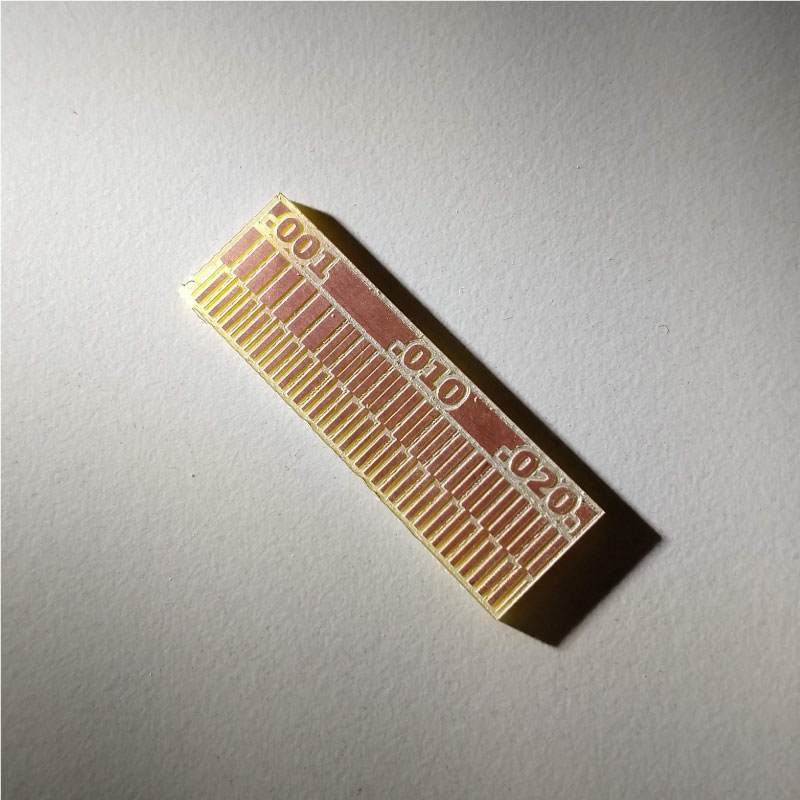
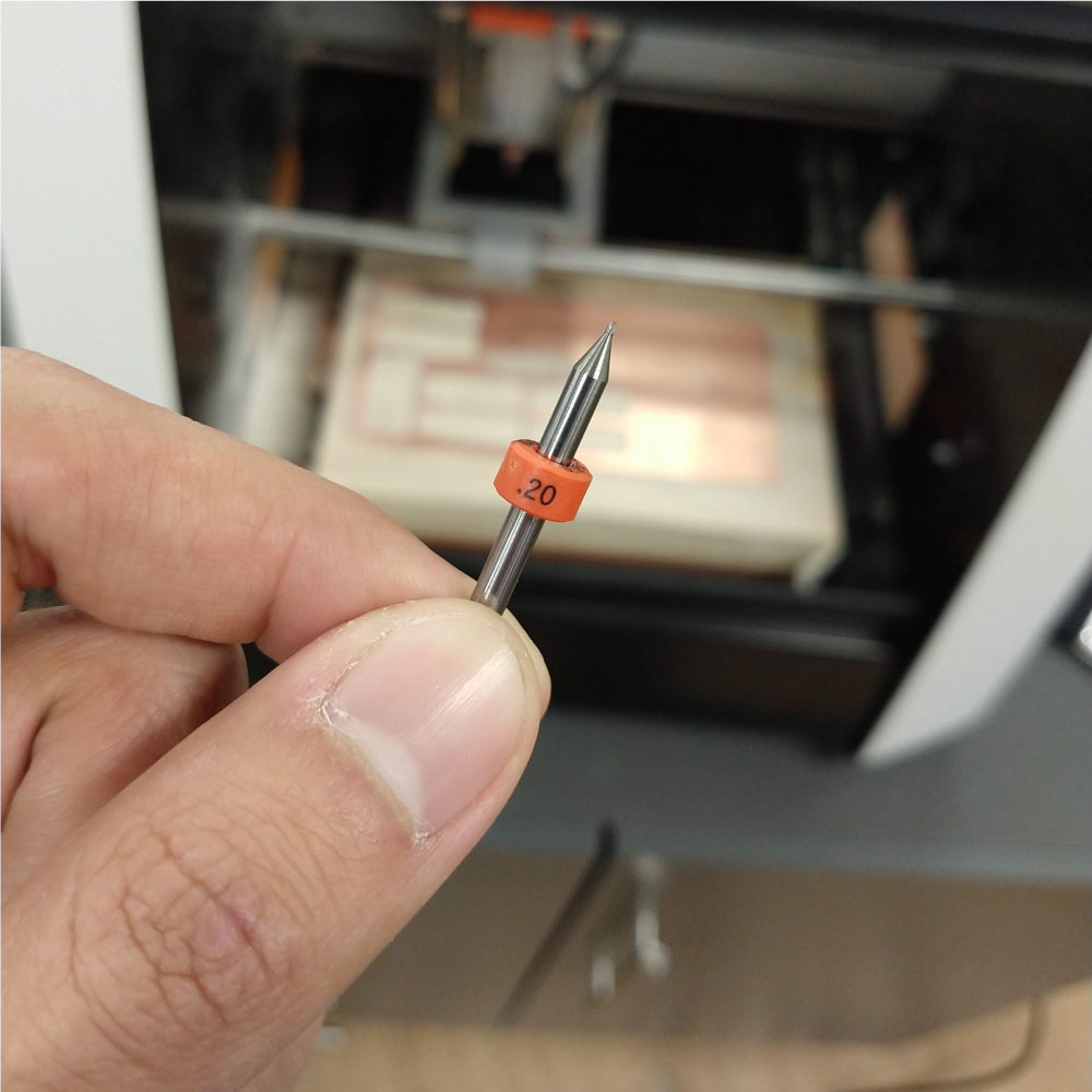
Roland SRM-20 PCB milling
Tool diameter: 0.20 mm Cut depth: 0.1 mm Max depth: 0.1 mm Offset number: 4 Offset stepover: 0.5 mm Speed: 4 mm/s
Tool diameter: 1 mm Cut depth: 0.5 mm Max depth: 1.5 mm Offset number: 1 Offset stepover: 0.5 Speed: 4 mm/s |
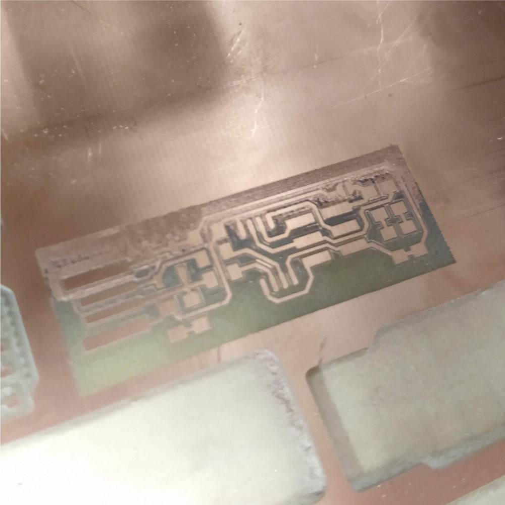
Got some problems with the cut depth but after a few tries I made it.
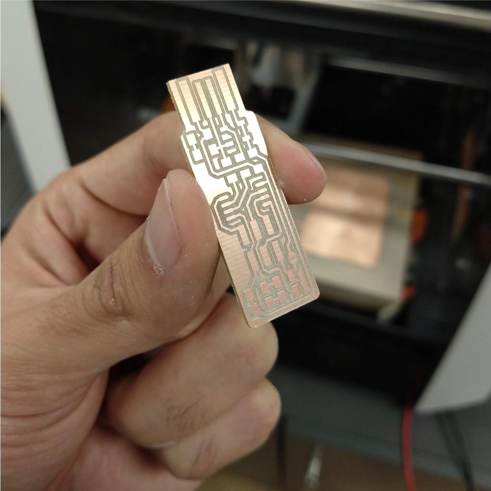
This was the result:
I also cut the line test board for the group assignment.
Soldering
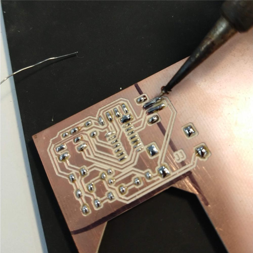
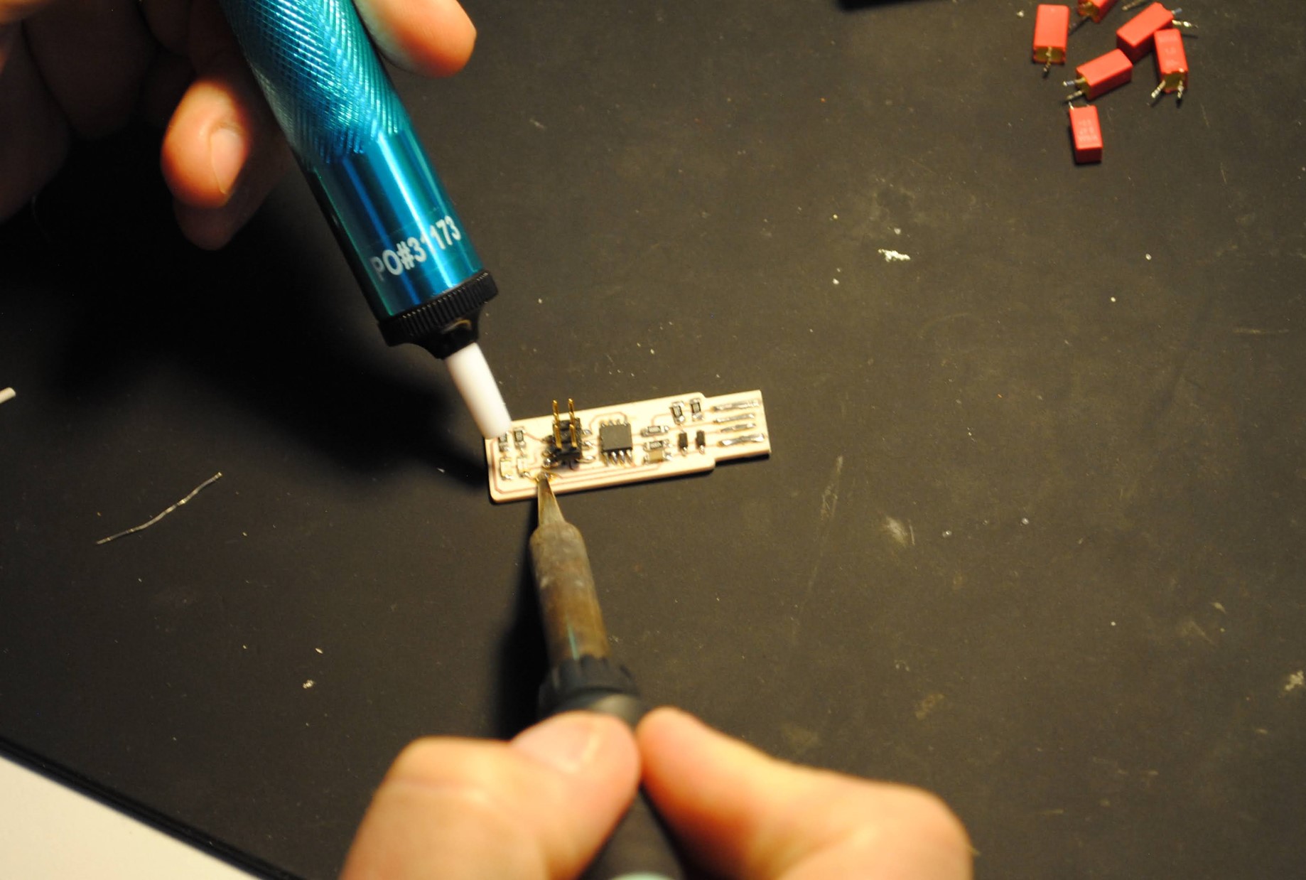
After cutting the board I had to continue with the most complicated thing for me: soldering. This is my first approach to electronics production, so I thought that it would take me a long time to place the components due to their miniscule dimensions, I would burn myself or burn the card with the soldering iron (preventing this situation I cut a couple of additional boards). Fortunately, with patience and following the advice of my colleagues, I did it in a short time.
To work comfortably, I placed the board in a stand with a magnifying glass, that way I had both hands free to hold the soldering iron and the solder. I deposited some solder on the pads one by one, as soon as the melted solder makes contact with the copper it adheres making a small bubble, ready to be heated again to join the components to the board.
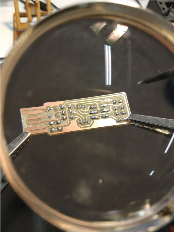
Fran Sánchez said in one of his videos that if you can read you already have half of the Academy done, and it is totally true. Taking the FabTinyISP diagram on the website as a reference, I began to place the components: first the microprocessor, then the small parts and finally the ISP header, which is very cumbersome and has many legs, following this recommended order I had no complications, unlike what I feared. I had to leave a couple of resistors pending because I did not find them at the time but I almost left it completely ready.
When I found the missing resistors I soldered them and started checking that the components were connected correctly using a multimeter. I only had one error: unfortunately the LEDs did not show current because I put them in the wrong direction, so I had to remove them and solder them again. I did this very carefully with some desoldering braid so as not to tear the copper tracks off the board.
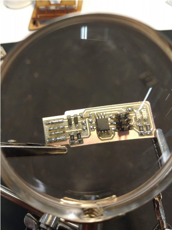
This is how my first PCB looks:
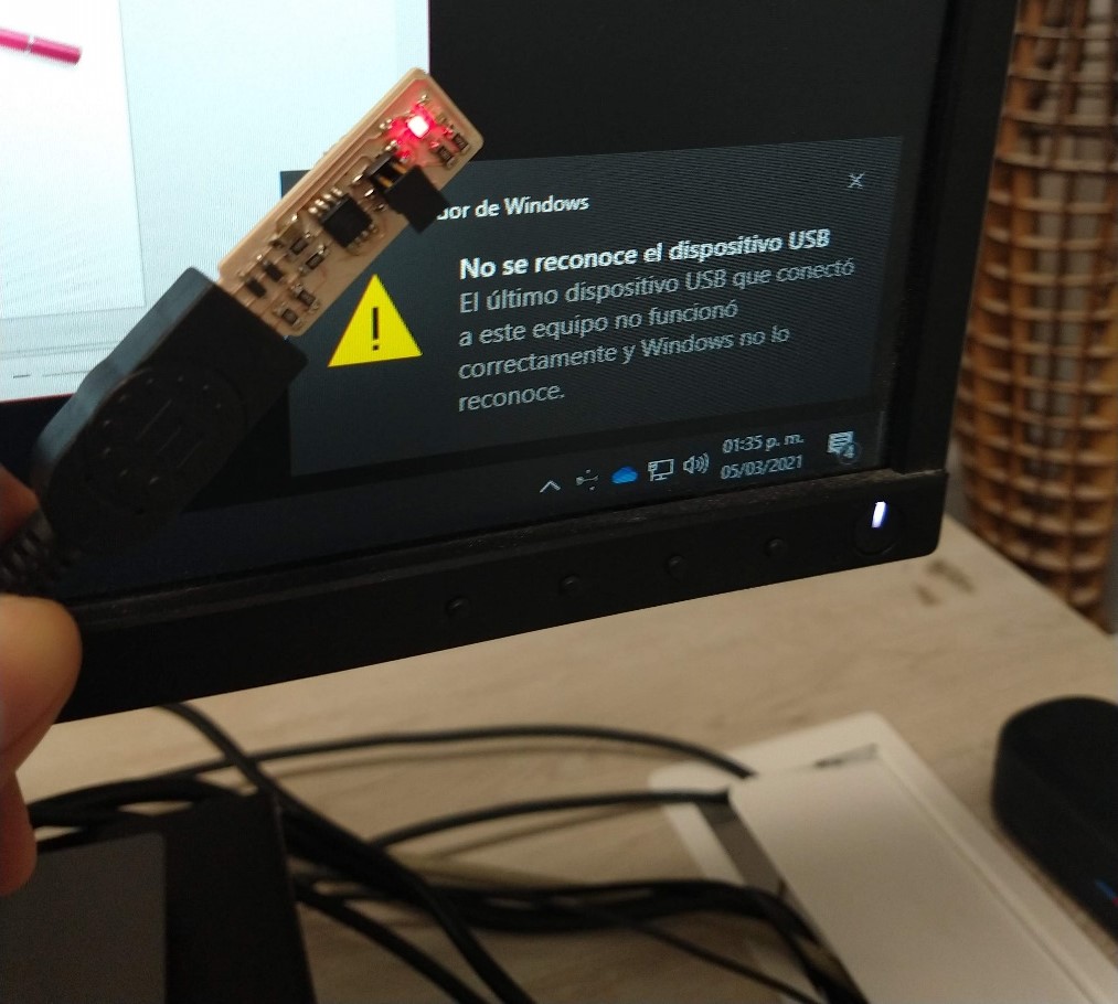
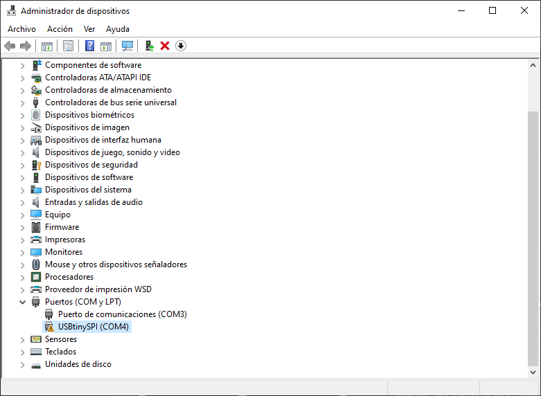
When connecting the board to the pc the red LED lights up, but the computer does not recognize the device in any way, so I guess I did something wrong. I am still investigating how to check my board.
The problems I faced
This is an assignment that I was very scared of as I am entering in a completely unknown terrain for me, luckily I learned a lot this week and all my mistakes and problems taught me a lesson.
-Correct height adjustment on the Roland Z axis is essential to obtain good results, in one of my tests the point of origin was slightly below the surface of the card which caused the bit to penetrate too deep into the material and the own diameter of the bit damaged the copper tracks.
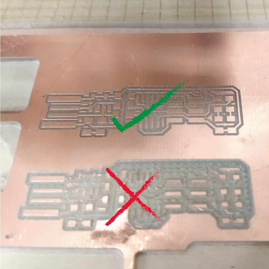
-A warped worktable or sacrifice board (even by fractions of a millimeter) results in poor engraving with roughly roughened areas. This can be solved by flattening the sacrifice board, setting a deeper depth of cut, adjusting the origin point in Z, or modifying the height of the bit.
-Adjusting the origin point in Z must be done very carefully, when lowering the bit it can break or even damage the spindle of the machine, to avoid this it is essential to manipulate the Z axis at a small feedrate (x100, x10 or x1). I moved the spindle very fast and broke the tip of the bit on a collision, but from now on I'll do it very carefully because I don't want it to happen to me again.
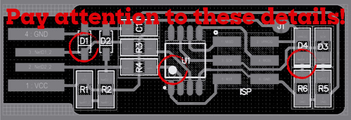
-The correct interpretation of the electronic diagrams is essential for the placement of the components, not only does it offer the location of each piece, it also indicates the direction of the polarity. If a component with two poles is placed incorrectly the circuit could fail like mine did because I had the LEDs placed backwards.
Adjusting bit height
In small parts such as a PCB, having a good resolution in the engraving is essential, to achieve this it is necessary to place the drill at the correct height: just over the surface of the material, not floating, not pressing. To achieve this I tried two methods:
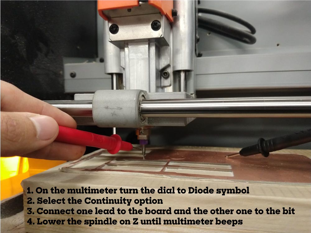
1. Using a multimeter in the continuity option. I connected one lead to the board and the other to the bit, slowly lowered the Z-spindle, and stopped as soon as the multimeter sounded its alarm. The materials of the card and the bit are conductive so when touched the circuit closes and the alarm sounds. This is a very accurate but complicated method to perform as it is difficult to keep both leads connected, lower the spindle on the PC program and keep the machine door open, at the same time. Using alligators and bypassing the door safety sensor can help.
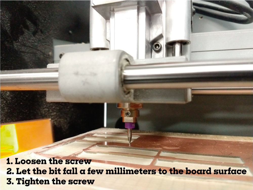
2. Using only the wrench to adjust the drill bit. I placed the spindle about three millimeters from the surface of the material, unscrewed the collet screw of the bit so that it could descend by pure gravity to the surface and at the point where it stopped I tightened again the collet. This is an easy method but must be done carefully as the bit could be damaged by impact.
Tuesday, March 2
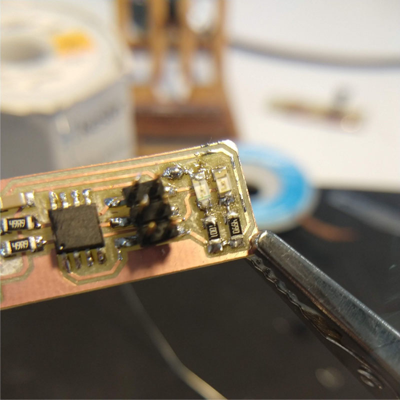
With the debugging recitation I learned some useful things so I tried today to find the problem on my board, but accidentally I ripped off some traces while removing the ATtiny. I'll make a new board this week.
Thursday, March 4
Today I made another board trying to avoid applying too much heat to the components as maybe that's why I damaged the processor on my first board. Everything seemed fine at the end but while testing the two LEDs were glowing at the same time. Trying to remove them I ripped the tracks again. I'll try again tomorrow.
Friday, March 5
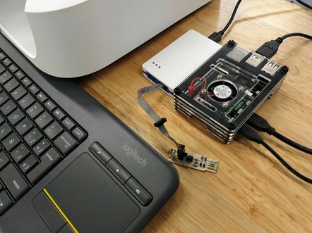
Finally I got a working board, it's getting easier as I practice soldering. To obtain a good result it is essential to do things with patience and looking for a way to work comfortably (the third hand is essential for this). My computer recognizes the board when I plug it in and it's ready to program other boards because I finally got the proper development environment using a Raspberry Pi. You can read the full story ony my embedded programming assignment.
We tried to program the board in Windows from different computers, we installed lots of applications to test without success, so we had to look for a Linux computer because apparently the development environment was much simpler using it:
-Linux
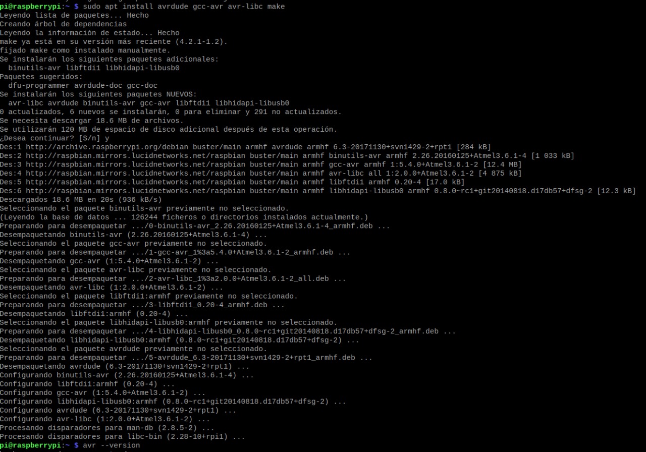
For Ubuntu and other Debian-based distributions, just enter the following command, followed by your password when prompted:
sudo apt install avrdude gcc-avr avr-libc make
-Windows
For Windows you have to:
- Install Git
- Install the Atmel GNU Toolchain
- Install GNU Make
- Install avrdude
- Update your PATH
- Install Drivers for your Programmer
- Do a Sanity Check
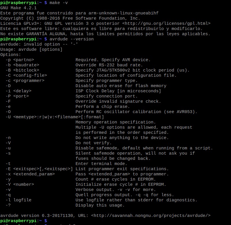
It is much easier to do it on Linux. As we didn't have any Linux computer (and a bootable USB did not allow us to keep the installed applications after restarting the computer), we tried using a Raspberry that we had on hand.
With the command sudo apt install avrdude gcc-avr avr-libc make the applications were installed on the Raspberry.
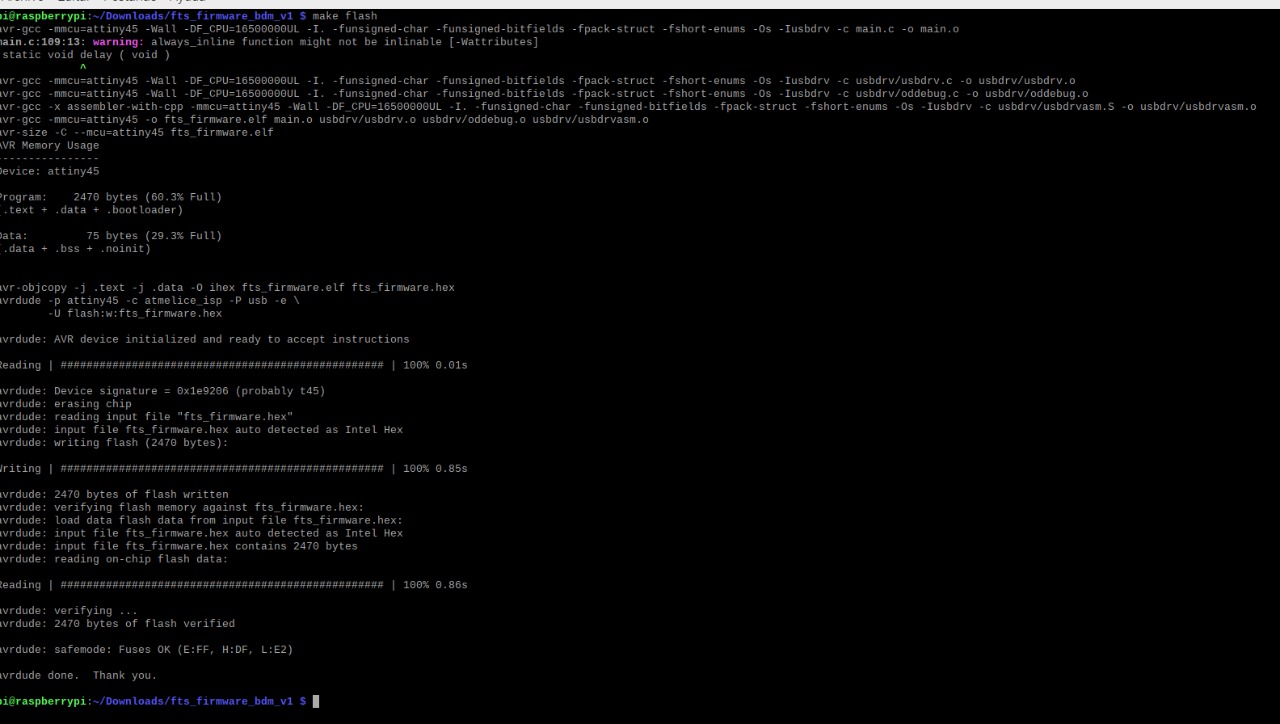
We downloaded the source code and extracted it to the root folder, executing the make command generated a .HEX file that will later be written to the chip.
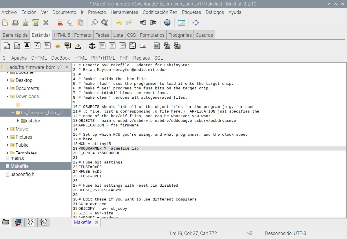
We edited the Makefile file to specify that the programmer we will use is an Atmel-ICE.
With the command make flash we erased the content of the chip and wrote the content of the .HEX file that we created earlier.
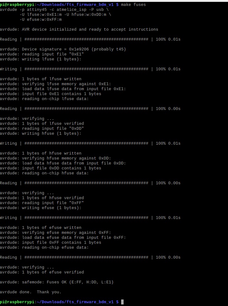
With the command make fuses we set the fuses that control where the microcontroller gets its clock source from.
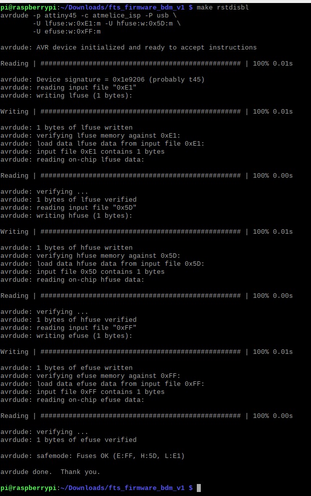
And finally we disabled the reset pint and turned it into a GPIO pin using the command make rstdisbl.
We physically removed the solder bridge that connects VCC with the programming pin.
To test the board as a programmer we uploaded a Blink sketch on my echo board.
|
For this assignment I:
|