Week 5 - electronics production
There is a lot to say about electronics. This week starts with electronics production. In the following sections we will talk about the Printed Circuit Board (PCB) fabrication technics, the materials used for milling, the board houses that offer services to make boards, the components of PCBs, the assembly methods such as soldering and the Computer Aided Manufacturing (CAM) tools used to edit the files that are sent to the milling machine.
PCB fabrication
Printed circuit boards (PCBs) are mostly made by etching or milling. This week we will only focus on the second process (milling). One reason is that etching requires a lot of chemicals that have environmental impacts and safety issues. The second reason is that there is a lot of set up for etching while there is almost none for milling. In this section we will talk about the two main PCB fabrication methods, the etching and the milling and also about other fabrication methods that are less used but allow to do funny things.
Etching
Commercially circuits are most of the time made by etching. It typically consists of graphically transferring an image using a photosensitive material by lithography and chemically etching the copper. This process involve nasty chemicals such as ferric/cupric chloride and ammonium/sodium persulfate. More can learned about the safety of using these chemicals by searching them on SDS, a platform registering material safety sheets. These are the standard sheets that tell you about safety of using different materials. In the case of the etching process, chemicals are hazardous to humans and to the environment. There is a note on the environmental impact of making circuits boards. It also consumes a huge amount of the water supply (approximately 1m3 of water to make 1m2 of circuit board). As a consequence this process would never be used without waste management. The disposal is very sensitive but the process can be very high resolution. It is therefore very valuable for making boards with very fine details. It is also a batch process used for big PCB production as it allows to make many boards at once.
Milling
Milling is the process that will be used for this week assignment. One asset of this process is that it produces no chemical wastes; it only requires a little dusty clean-up from machining. It is not recommended for the highest resolution nor batch production but it's a great process for prototyping. Note that breadboards should never be used for prototyping because they have a lot of parasitic capacitance and its electrical performance is different than a real PCB.
There is a series of videos explaining the whole process. It is done using a little desktop milling machine such as the Roland SRM-20. Of course the precision of the work depends on the milling machine but it also depends on the end mills. End mills come in several sizes. 1/32, 1/64" and 1/100" are the most common sizes. A 1/32" end mill cuts out the outline and makes the holes, a 1/64" end mill makes the fine traces and a 1/100" is used for finer traces and very specialized parts. There are also biggest end mills usually used to cut the edges of the board after the circuit engraving. The smaller the size, the finer the work is but the process will also take more time.
To fixture the board, rather than using a clamp, the board is paste to the working area of the machine with a double sized tape or a backing that has a weak adhesive (Permacel #595B). The reason to do that is that when the board is clamped from the sides it can bow a little bit and if the board isn't flat it has tension in it that might break the end mill. With an even layer of adhesive the board is maintained flat and without inner tension. Between the board and the bed of the machine there is an underlay, a piece of material that is sacrificed to protect the integrity of the bed when the end mill cuts through the board. This underlay has a lifetime and must be replaced periodically. Also note that if the material is a little bit wrapped there is also a software solution to solve that issue, for instance AutoLeveller.
Another important thing to do before milling is zeroing the tool. Depending on the abilities of the milling machine, the zeroing can either be manual or automatic. This procedure allows the machine to know exactly at which height the end mill is touching the top of the board. When it is done manually it is worth to put a little bit of pressure on the end mill. It avoids the end mill to climb when tightening the set screw. If the screw small try to not tighten it too much otherwise it might damage the screw thread.
When milling a PCB the end mill rotates clockwise and its direction can either be of two types: climb direction or conventional direction. With conventional machining the cutting pulls the tools in towards the stack. Climb machining pulls it away from the stack. Generally climb machining produces cleaner cuts because it can make a good bite in the stack and releases it on the surface contrary to conventional machining that bites at the bottom where it is hard to start and releases it where it does no longer matters.
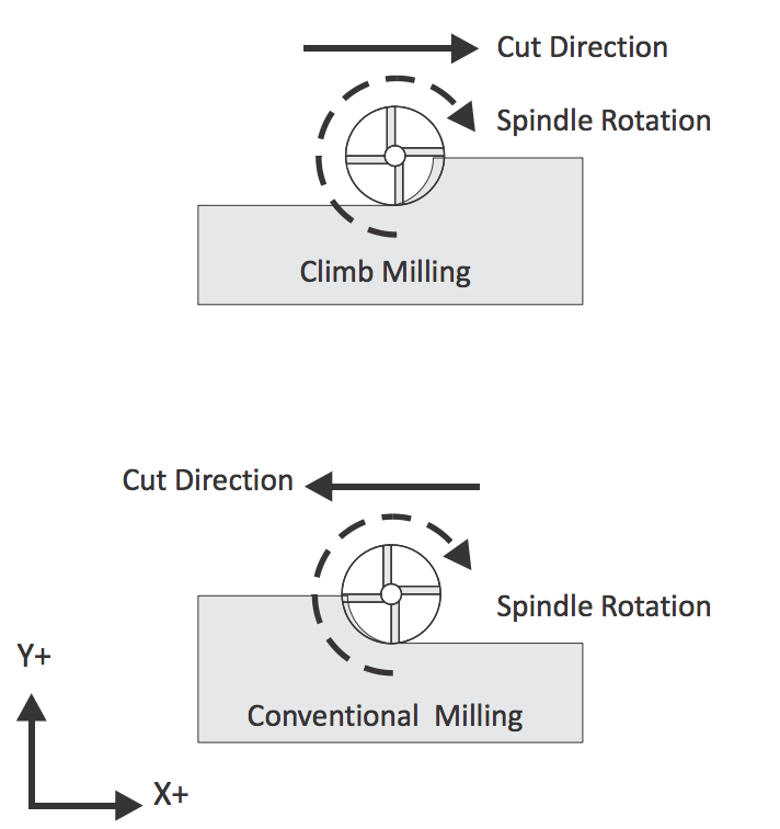
Climb vs. Conventional Milling
When the milling is done it might be worth to remove the surplus of copper that lays on the edges of the board. This operation is called the deburring. It is easily done with a sharp edge. Some cleaning might also be needed. For example the oil of the fingers can etch the board overtime. To avoid that issue the board can easily be washed in soap water.
Other methods
With a vinyl cutter and a copper tape it is possible to cut electronic circuits. Their main asset is that it allows to do flexible electronic circuits. This solution can also be used for esthetic purposes by encapsulating the circuits in clear epoxy to get a transparent board. More than being esthetic the epoxy function is also structural, it strongly maintains the components on the board. Note that another solution to have flexible circuitries might be to cut the copper tape with the milling machine.
Fiber laser can also be used to make electronic circuits if you are fortunate enough to have one since the equipment is quite expensive. Some research is also made on printing electronic circuits. Another method is Electroplating. It consists of printing a poor conductor on the board and then using a bath to electroplate it. The last method we will talk about is sewing. It uses conductive threads to sew circuitries at lower resolution with a sewing machine.
PCB materials
Rigid boards
We most used materials are FR4 (epoxy glass) and FR1 (phenolic paper). FR4 are glass reinforced boards and therefore cannot be used in a milling machine. Instead FR1 is used since it is a fiber reinforced board that machines beautifully.
Flexible boards
Commercially flexible boards are done with Kapton. It is very expensive. A cheaper solution is to use an epoxy film and a copper foil with the vinyl cutter.
Other substrate
Window glass and Teflon are good substrates to make high-frequency circuitries.
Board houses
When there is hundreds of boards to produce it does not seem reasonable to craft them one by one by machining. A worthy solution might be to send the design files of the board to a board house:
- PCB:NG
- AP Circuits
- Advanced
- Sierra
- Screaming Circuits
- AQS
- Gold Phoenix
- 3PCB
- Seeed
- PCBWay
- JLCPCB
- Think & Tinker
The cost of the board and the time to make it depends on a number of design rules. One of them is about the width/spacing of the traces. While milling the traces a typical value for the traces width or the spacing between them is 15 mils (15 thousandth of an inch). Board houses can decrease this value until 5 mils. Below that value the circuit is called a high density interconnect and that is a more expensive and less conventional process. The cost of the board will also depend on its complexity. The more layers it has the more complex it is. For example the board of a smartphone can go up to 10 layers or more.
Several layers must be sent for fabrication to the board house. There is one for the traces, a mechanical layer for the boundaries, a drill layer if holes are needed, a solder mask which controls where the solder can go and then there is a silk screen that has the graphics on the board. To connect these layers there are via. In addition there are blind and buried via. Blind via are connections between the surface and one internal layer and buried via are connections between internal layers. When making a via conductivity is required from the top to the bottom. This can be done by electroplating or by the use of rivets or jumpers.
Components
Octopart is a search engine for parts. When looking for the ATTiny44a one can notice that the microchip can come in several package: DIP package, Surface-mount package and chip scale package. DIP chips have leads that go all the way through the board. It only make sense to use them when its mechanically needed otherwise they can be replaced by Surface-mount parts where the leads are just on the top side. Chip scale package are a denser version of surface-mount parts where the leads don't even stick out but are underneath the component.
Assembly
Soldering
Soldering is the method used to stuff a board with electrical components. It sounds like an easy topic but it takes quite a while to master soldering. There is a thousand of different kinds of solder. Solder is eutectic. It is a mix of alloys each having a melting temperature. At an intermediate composition there is significant depression of the melting temperature that is called eutectic. Soldering is a surprisingly subtle process. When its is well done all the joints are shiny and smooth. Bad solder joints are not shiny and smooth, they are quite of greyish and bumpy. To make a good solder joint they are some recommendations. First, the tip of the soldering iron must be fine and clean. To clean the tip, melt a drop of solder on it then wipe it on a wet sponge. Then, bring the tip of the soldering iron at the intersection of the parts that must join to heat both sides. Then add a little bit of solder at the intersection, it helps for heat transfer. Wait for 5 or 10 seconds then gently probe with the solder to see if it flows on the traces. When the solder flows remove it but let the iron there a few seconds longer to allow the solder to keep flowing. Once it is done remove the iron away. All of that happens in about 15 seconds. The solder has a solder has a flux core that helps to clean the joint and let the solder flow. Some people like to add flux to help the soldering.

Good vs. bad solder joints
Another kind of soldering is reflow. With this technics little bumps of solder are placed separately on the each pads of the components. Afterwards the components are aligned with the traces of the circuits where it should belong and then placed in a oven or heated with a hot air jet to make the soldering. Drag soldering is another kind of soldering. This technics is used for parts that have very close together traces. It consists of putting flux on the pads, put solder on the iron and rub it back and forth. Finally wave soldering is an industrial process that enables one to manufacture many circuit boards in a very short amount of time. It works by passing each circuit board over a pan of molten solder. A pump in the pan creates a "wave" of solder that washes over the board, soldering the components to the board.
Stuffing
Stuffing is the operation consisting of placing the components on the board. One important topic about stuffing is the components orientation. Some components such as diodes or chips (chips have a dot for pin 1) have an orientation and its is important to respect it when stuffing the board. It is important to respect a certain order when soldering. Try to start from bottom to top and from inside to outside. Try also to use a good tweezer to place the components where they belong and use a little bit of solder as an adhesive to stuck them in place.
When mistakes have been done when soldering it might be needed to desolder the parts. This can be done by using either a braid, a vacum desoldering pump or a hot air gun with the help of gravity to pull it away from the board. If after the production of the board it appears that there is a mistake and that there is a trace somewhere that should not be there, that trace can be removed by cutting it with a sharp cutter. At the opposite if a trace is missing a jumper can be added to correct the mistake.
There are also pick and place machines that can stuff a board and solver the components without any help.
After stuffing the board comes the last step of the fabrication: the encapsulation. This step might be needed if the board must be robust against the environment. It can be done with clear epoxy as already mentioned earlier but it can also be done using silicone in sprays or dips.
CAM - Computer Aided Manufacturing
CAM software helps for computing the tool path of the milling machine. The most common format to communicate with the machine is the Gerber/RS-274X format. It is an historical bizarre format originally created for early sawing machines and photoplotters based around flashes and masks. Instead another format that is more convenient to share PCBs schematics is a Bitmap such as the PNG format. Nevertheless make sure that the picture is not a low resolution picture. It is important that the picture that is sent for milling has the resolution of the machine. Typically if the machine has a resolution of a thousandth of an inch and the board is a few inches with a resolution of a thousandth of an inch, then the picture is only a few thousand pixel which isn't very large and quite convenient for sharing files.
There is a number of workflows to generate the paths but mods is sufficient and very effective to generate the G-CODE.
FAB ACADEMY 2020 source
20200219 Electronics Production from Academany on Vimeo
My Assignment
This week again there were one group assignment and one individual assignment. The group assignment consisted in characterizing the design rules for the PCB production process. To do that we used a template provided by Neil, we generated the G-CODE with mods and milled it on a single-sided FR-1 PCB blank with the Bantam Milling Machine using two different drills for the engraving: 1/64" and 1/100". Afterwards we looked at the minimal width for which the traces precision and quality were still acceptable.
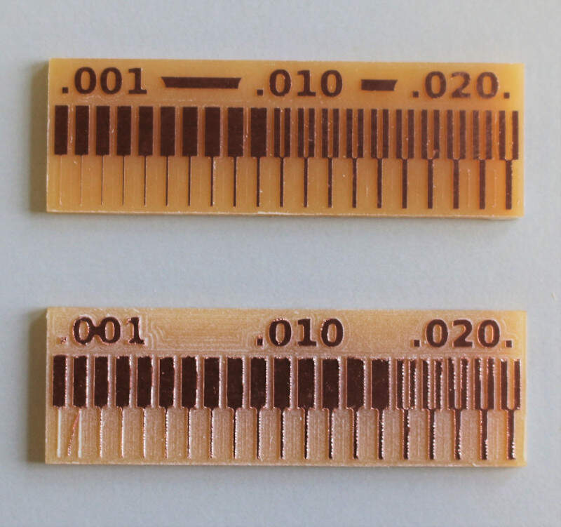
Line test engraved with a 1/64" and a 1/100" End Flat Mill
This individual week assignment consists in making an in-circuit programmer by milling and stuffing the PCB. The following section aims at describing the production process.
Software
- mods - This week mods has been used to generate G-CODE files for the milling machine and to vectorize PNG files for the vinyl cutter.
- Bantam Tools Desktop Milling Machine Software - This is the user interface of the milling machine.
- Inkscape - Inkscape has been used to edit the DXF files for the vinyl cutter. More information about files editing for the vinyl cutter is provided in WEEK 3.
- Silhouette Studio - Silhouette Studio is the user interface of the vinyl cutter.
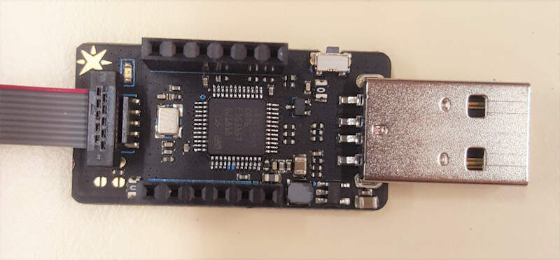
- EDBG - EDBG is an open source simple utility for programming Atmel MCUs though CMSIS-DAP protocol. It works on Linux, MAC and Windows. For installation, download the last Binary release and copy the .exe file in the folder of your choice. To run the program: open a command prompt, change directory to the location of the Binary release and write a command starting with the name of the .exe file.
Machine
Bantam Tools Desktop PCB Milling Machine
The Bantam has both a power switch and an emergency button. It also has an exhaust system connected to a filter. This extractor must be turn on while milling the PCB.
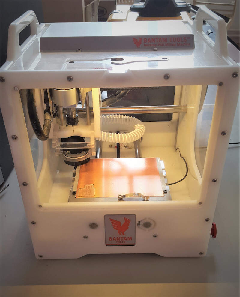
Bantam Tools Desktop PCB Milling Machine
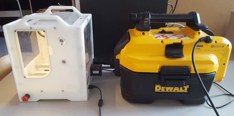
Extractor with filter of the Bantam
Silhouette CAMEO 4 PLUS
This week our FABLAB made the acquisition of a new vinyl cutter: the Silhouette CAMEO 4 PLUS. Getting started with this machine is as easy as with the previous one. If one is interested to know more about how to start with it more information can be found here.
Work flow
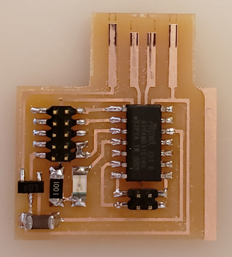
Among the prerequisites to make a PCB having the sketch of the electronic circuits at disposal first is essential. Fortunately a collection of in-circuit programmers drawings was provided for this week assignment. Thus before starting my assignment I asked to my local advisors which board might be the most useful for the next weeks. On their advice I decided to mill the ARM CMSIS-DAP.4.D11C and the ARM CMSIS-DAP.10.D11C.
CMSIS-DAP.4.D11C
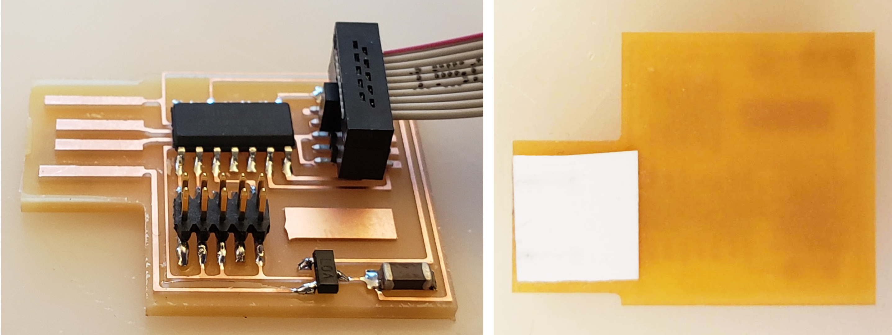
CMSIS-DAP.10.D11C
The electronics sketches provided to make the circuits are a PNG file that precisely describes the value and the position of the components that will be stuffed on the board, a picture of the final product, a PNG file with the traces of the circuit and another PNG file that indicates the limits of the board.
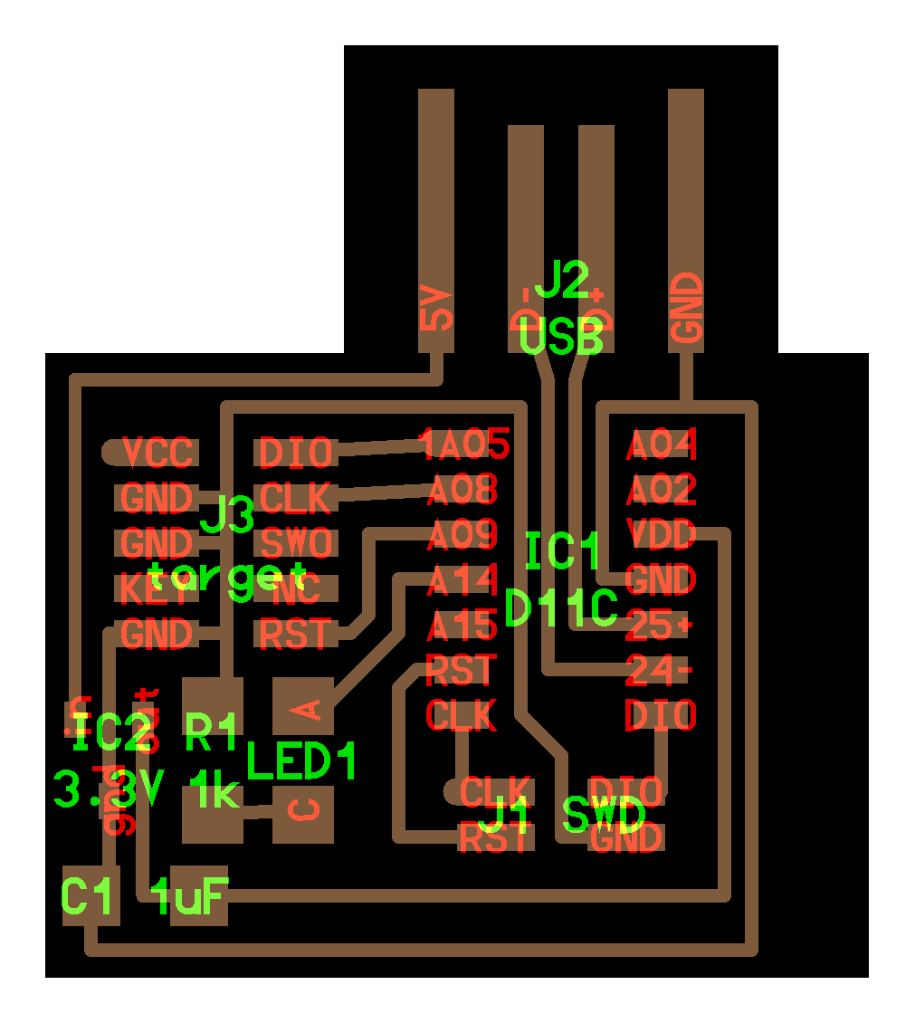
Schematics of the CMSIS-DAP.4.D11C
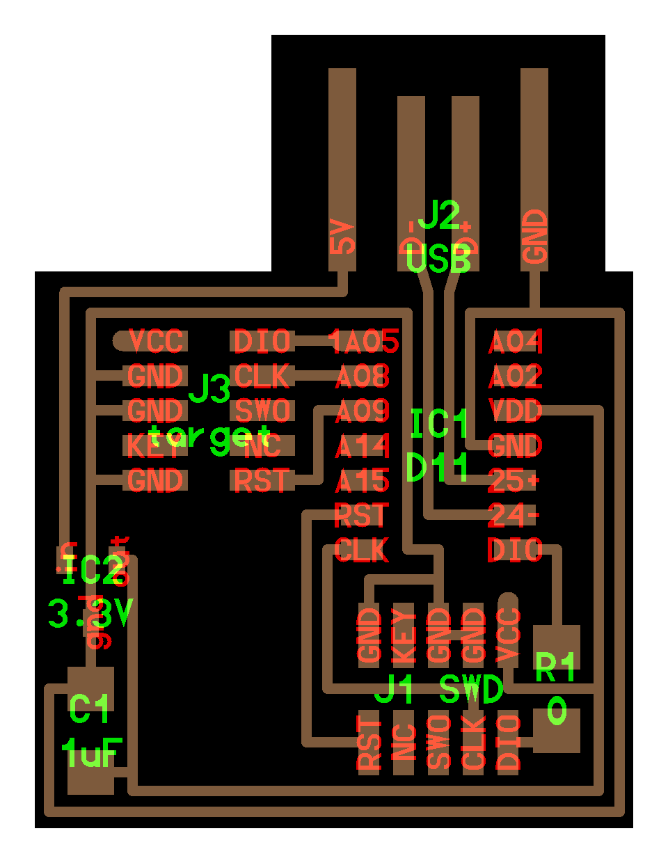
Schematics of the CMSIS-DAP.10.D11C
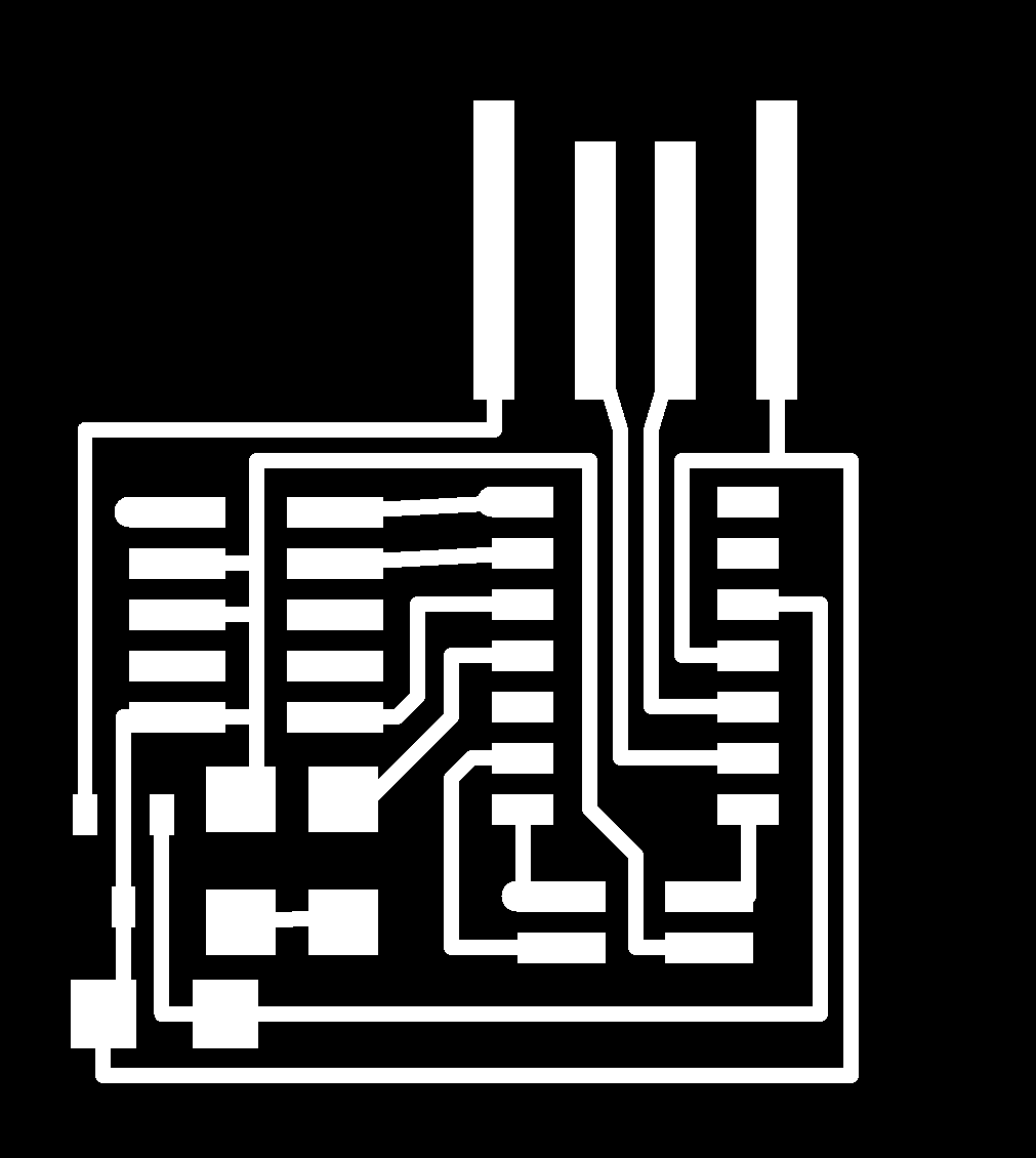
Traces of the CMSIS-DAP.4.D11C
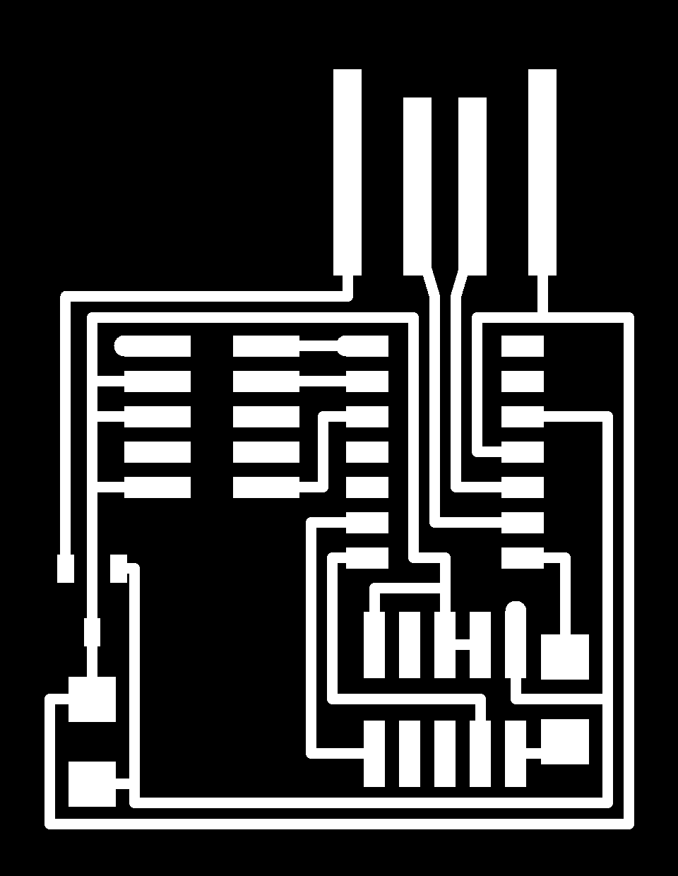
Traces of the CMSIS-DAP.10.D11C
Interior of the CMSIS-DAP.4.D11C
Interior of the CMSIS-DAP.10.D11C
As usual these files must first be prepared before using them. In the following section I'll explain two different fabrication methods. Afterwards I'll focus on the stuffing and the soldering. Finally I'll talk about the programming and the testing.
Board fabrication
In this section I'll explain two different fabrication methods each producing a different type of board. The first method I used requires the milling machine. With it I made a rigid version of the CMSIS-DAP.4.D11C and CMSIS-DAP.10.D11C boards. The second method requires the vinyl cutter that helped me to build a flexible version of the CMSIS-DAP.4.D11C board.
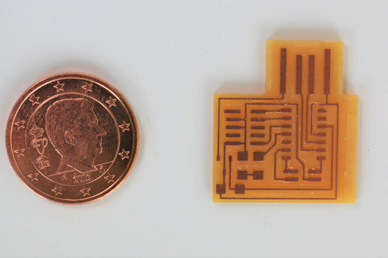
Rigid board
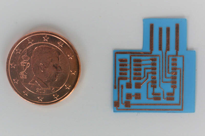
Flexible board
Rigid board with a milling machine
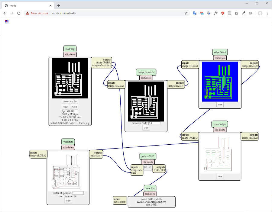
In this section I'll only focus on the fabrication of the CMSIS-DAP.4.D11C board since the procedure is the same whatever the board schematics is. First the files provided has been prepared for milling. This has been done with mods.
Before going deeper into Mods let's fix the blank copper PCB board on the bed of the milling machine. To do that I cut several bands of double-sided tape that I uniformly distributed on the back of the single-sided blank copper PCB.
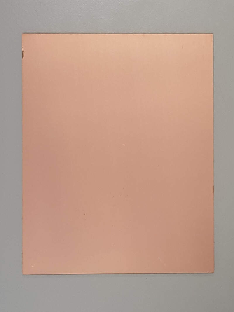
Blank copper PCB
Preparation of the PCB

1/100" Flat End Mill

1/64" Flat End Mill
It is time now to use the user-interface of the Bantam. First the tool must be specified by selecting "Change..." in the right-side "Configure" menu. Select the name of the tool.

Then click on "Continue". It will run a calibration procedure for zeroing the Flat End Mill. After this procedure, it is possible to know exactly the height of the blank copper PCB by selecting in the top menu "Bitbraker -> Probe material thickness". Before clicking on "check thickness", make sure the electrical contact is made between the machine and the blank copper board. Then click "accept thickness". In this case, the thickness is 1.74mm. This value makes sense. Therefore I clicked on "accept thickness". This value will be very important to generate the G-CODE that will cut the edges of the board. For this G-CODE the max depth will be equal to 1.74mm - 0.02mm where 0.02mm is a safety margin to prevent the end mill to cut in the bed.

In Mods, right-click in the window and select "programs -> open server program -> processes -> mill -> 2D".

Then add the "G-CODE" module ("right-click -> modules -> open server module -> path -> formats -> g-code") and the "save file" module ("right-click -> modules -> open server module -> file -> save").

A faster solution is to directly select "programs -> open server program -> machines -> G-code -> mill 2D png" after right-clicking in Mods.

In the "read png" module click on "select png file" and choose the file with the traces. In the "mill raster 2D" module set the tool diameter to 1/64" = 0.396875 mm, to 0.01" or to 1mm (for cutting the board) depending on the tool used, the cut depth to the half of the max depth (for 2 infeeds) and the max depth to 0.14 mm for removing the copper layer and to 1.72mm to cut the board. Set the offset number to 10 when engraving or 1 for cutting. It is the number of path successions around the traces. When the offset stepover is equal to 0.5 the paths overlay at 50%. The other parameters are shown in the pictures below.


Once the G-CODE was generated I loaded the file in the Bantam user interface. An error occurs with the message "Unsupported G54".

To solve it I just commented the line G54 in the G-CODE and reloaded the file in Bantam user interface.

Then I clicked on "Start Milling...". Note that, at this point, the machine was milling at a very slow speed in comparison to what I expected. I noticed there might be a problem with mods and the feed rate setting. In fact, the issue was due to the units that were obviously not in mm/s but probably in inches/minutes. Indeed I expected a feed rate of 200mm/s but if instead the units where inches/min it meant that I had entered a feed rate of 200 inches/min = 84.6 mm/s. By making the appropriate conversion I fixed the problem and generated a new G-CODE.


After a few minutes the board was finished and almost ready to stuff.
Flexible board With a vinyl cutter
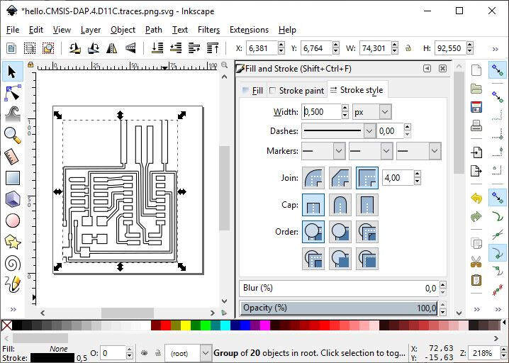
Hereinafter are the different steps I followed to make a flexible board. First I vectorized the PNG file with Mods. First I right-clicked in Mods then I selected "programs -> open server program -> image -> vectorize". After I edited the SVG file for cutting in Inkscape (this procedure is explained with more details in WEEK 3) and I saved it as a .DXF file.
Vectorization of the traces with mods
Editing of the .SVG file with Inkscape
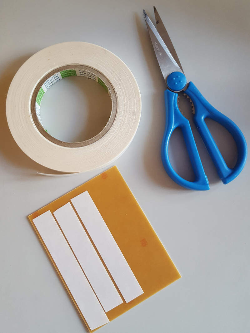
I made several tests in Silhouette Studio to find the right force, speed and thickness for the cutting and I found the following values: speed = 5 ; force = 30 ; thickness = 1 tenth of mm. Once the copper tape was cut I used the following material to transfer and weep it on its final flexible substrate.
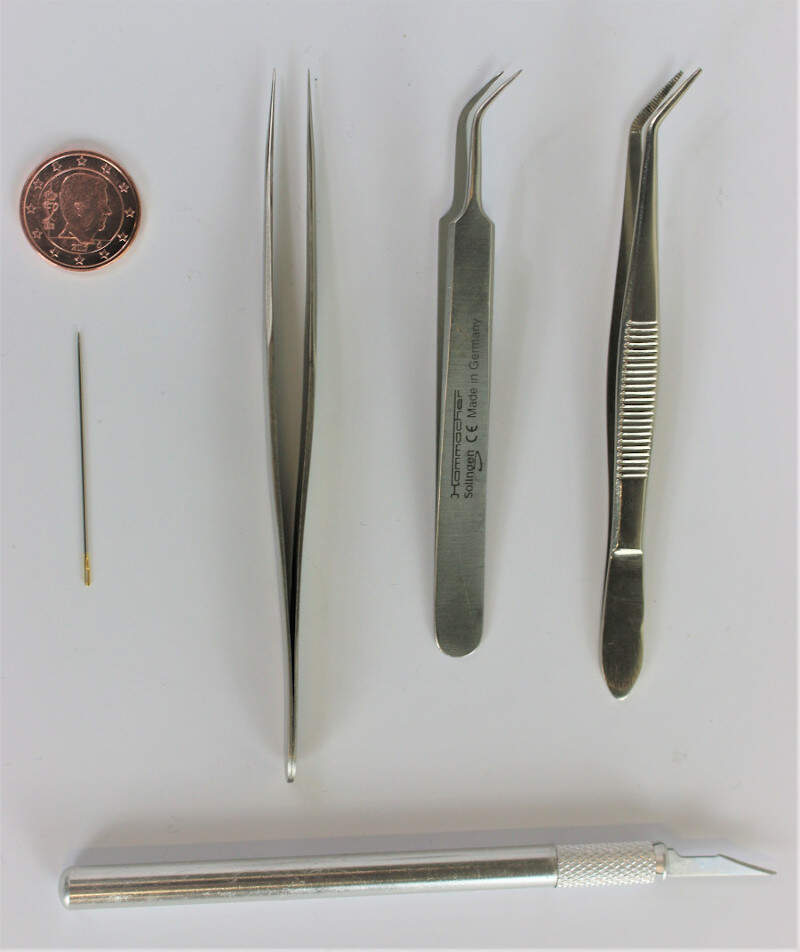
Material used for transferring and weeding the copper tape on its definitive substrate
To transfer the circuit I used a tape with a weak adhesive. Then I removed the protection of the tape and I paste the copper on the final substrate. I used a coin with the head of King Philip of Belgium to scratch the copper on its final substrate and make sure it is strongly pasted on it.


Finally I used tweezers to weep the parts of copper that had to be removed. It was not easy. It was quite intense because I had to be very careful when weeping around the very small traces. I felt really relieved at the end when I was able to finish the work without to much trouble and a very satisfying result. Thank you King Philip!
My flexible board before stuffing
Stuffing and soldering
Before stuffing I used sandpaper and soap water to clean the boards (only the rigids ones). I looked at the schematics of the board to know which components I had to use. The list of the material is the following:
- One ATSAMD11C - Here it is an ATMEL ATSAMD11C14
- One 1kΩ Resistor
- One 0 Ω Resistor
- One diode
- One 1µF Condenser
- Two SWD connectors
Then I set the temperature of the soldering iron the 360°C. When starting to solder a component I first put a little drop of solder on one trace then I aligned the component and maintained it with tweezers in front of the trace while heating the drop of solder. Once I removed the iron, the component was fixed and it was easier to solder the rest of its pins.


To know the orientation of the diode, I used a voltmeter with its cursor aligned with the diode symbol. In that position, this voltmeter is also very useful to check that there is no shortcuts in the circuit and that the soldering is properly done.

Here we can see that the diode lights on when the negative born of the voltmeter is touching the side of the diode targeted with a little dot. This side must be connected to the ground.

To know the orientation of ATSAMD11C there is a little dot that indicates pin 1. In the schematics pin 1 is identified by a 1 in front of its name.

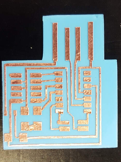
The first board I made was a failure but the more I practiced the more confident I felt and I'm quite happy with the final result of my three boards. One can also notice that it is easy to solder a rigid board then a flexible once because the latter was melting if I stayed too long with the iron on the traces.

Programming and testing
If there is no error in the previous parts, the programming of the boards is straightforward. The binary file to load on the DIY programmer is provided by Neil. This is done by using the commercial programmer of the FABLAB with the last Binary release of edbg. Make sure that the executable file and the binary release are in the same file.
First connect the JTAG commercial programmer to your computer via USB.
Commercial JTAG programmer
Then connect the commercial programmer to your DIY JTAG programmer.
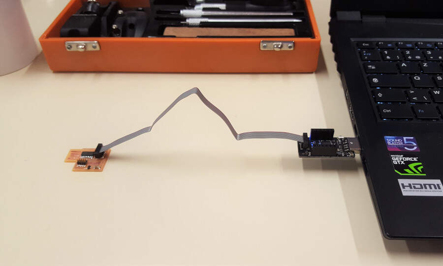
Connection between the commercial programmer and the DIY programmer
Open a command shell and use edbg. Make sure that you are in the same folder than the executable file. You can run the help command to learn more about edgb.
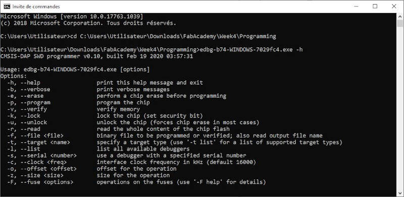
help command with edbg
You can list the supported target types. Here my target type is SAMD11.
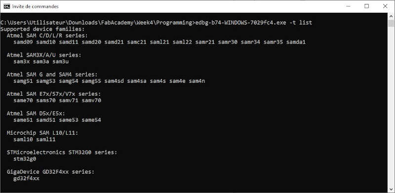
List of supported target types
By running the following command my DIY programmer has been successfully configured.
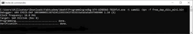
Configuration of the board as a programmer
Finally to test my programmer I connected it through USB to my computer and I used edbg to configure another board with mine. The test was successful. As a consequent I concluded that my board was operational!