Week 6 (Electronics Design)
Week 6
The proper way to measure current is in series. To do this you have to connect the multimeter’s probes in the correct ports. In this case we are going to place the RED probe on the mA port to have more accuracy and because the components I’m measuring has a low power consumption. This doesn’t apply to motors. Black always goes in COM. Now to measure current you need to make sure you are measuring DC current on the multimeter and you have to interrupt the circuit and use the multimeter probes to close again the circuit.
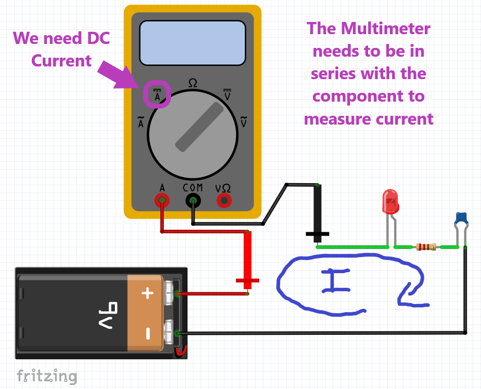
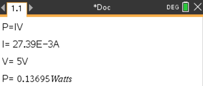
Remember that component that are in series share the same value of current. In this case we need current because we have a fixed voltage value. In this case its around 5V because that’s the output voltage of the FTDI cable I’m using.
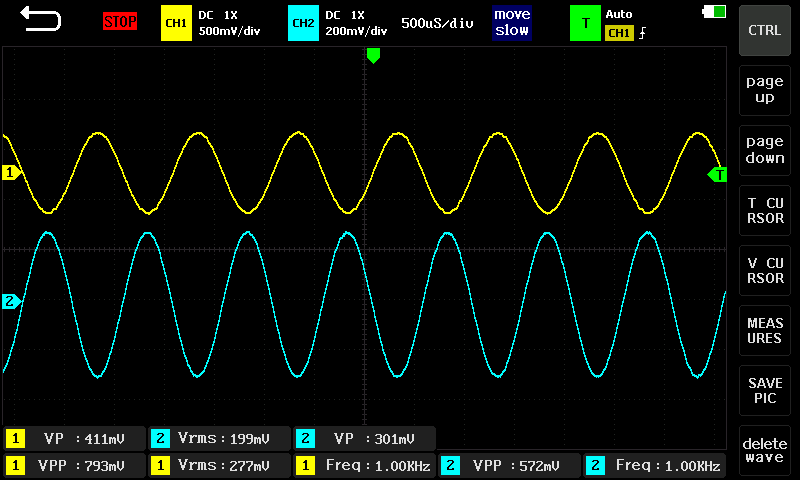
I own a Digital Tablet Oscilloscope that is amazing for students that want to learn how to use one and need something really portable to carry with them. This tablet brings 2 marching probes that look a little different compared to the multimeter probes but the work exactly the same with a positive (hook at the end of the probe) and a negative (alligator clip on the side wire). The placement will depend on the segment of the circuit you want to analyze. In my test we need to place the probes on the output of the PCB and see a squared signal that will vary its frequency when I move a potentiometer.

The oscilloscope graphs electronical signals as a waveform to show how the signal changes over time. Oscilloscopes gives us more information than a multimeter like Vrms, Vp, Vpp frequency and more (depends on the capabilities of the oscilloscope you’re using). The following picture is a screenshot from the oscilloscope measuring two signals simultaneously.
Week 6
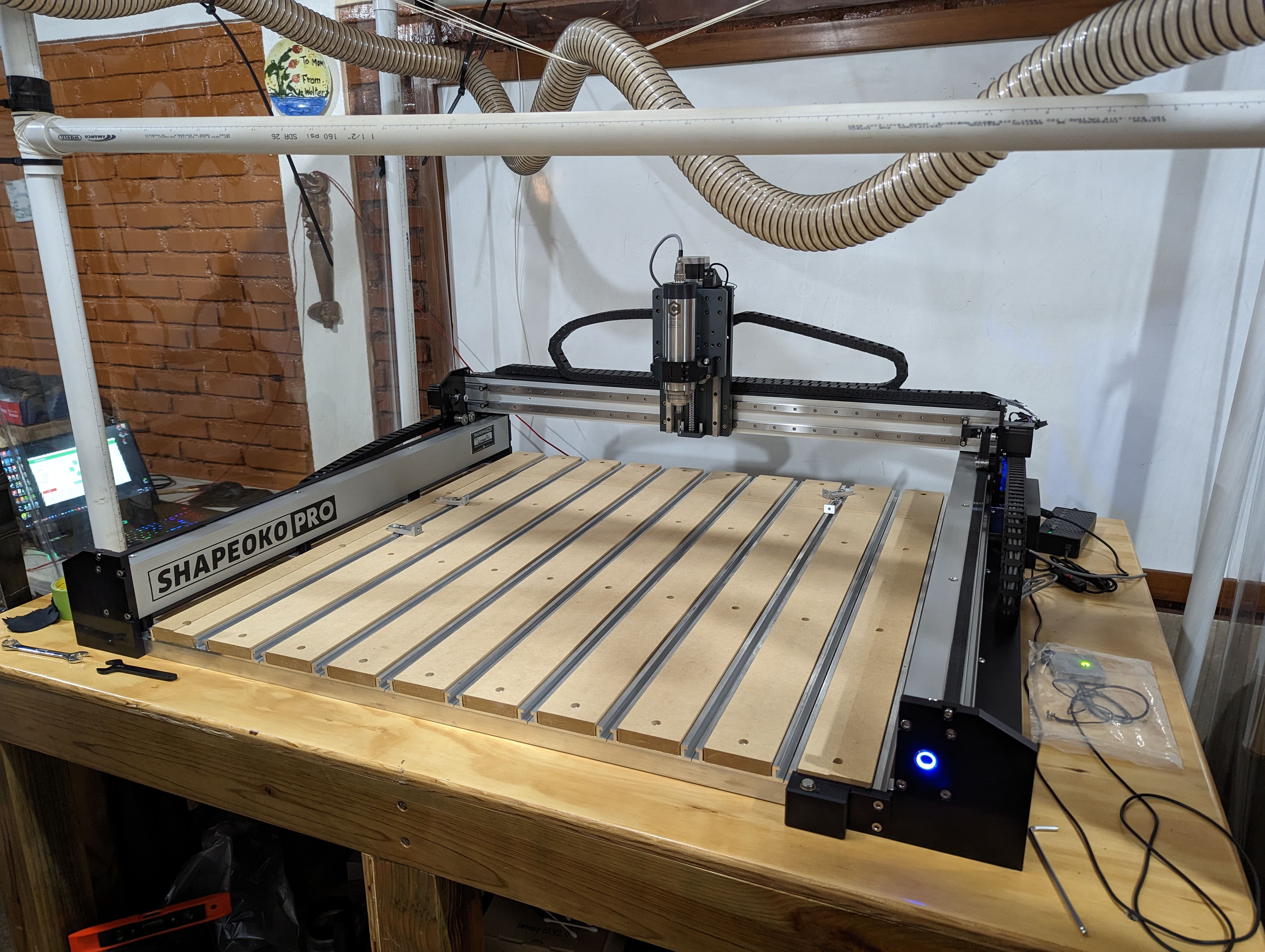
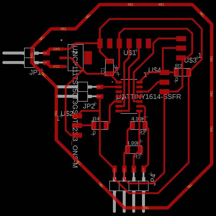
Do to the global and local problems I don’t a lot of choices for MCU selection. I have a limited amount of ATtiny 1614. I’ll make a PCB that has I2C communication, servo motor pins, and pins for a sensor. To make this PCB I’ll be using my Shapeoko Pro. Then I jumped in eagle to make the schematic and trances for my PCB. After finishing this I exported the trace to a png file.
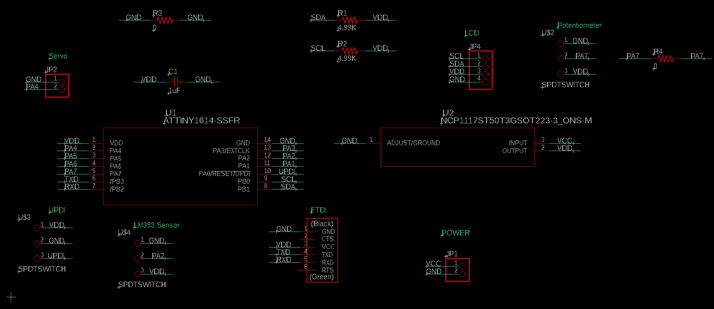
In the design process of this PCB, I received a lot of support from my friend/instructor Adrián Torres . I also studied a lot his Adrianino. In my PCB prototype I needed to gain more hands-on experience to add the appropriate modifications if needed. For started I added some pins to power the board with a battery if needed, FTDI port for serial communication with my laptop and 5V input, I2C port for easy connectivity with a variety of input and output devices, and easy access to UPDI port for programming. Thanks to a mod made by Adrian we can program the PCB with only 3 pins. No need to connect the FTDI for power while programing the board.
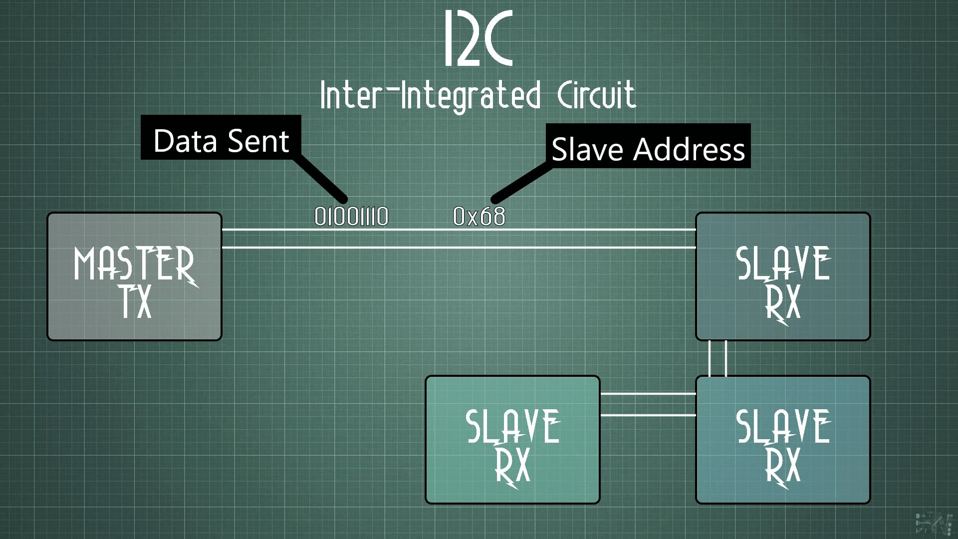
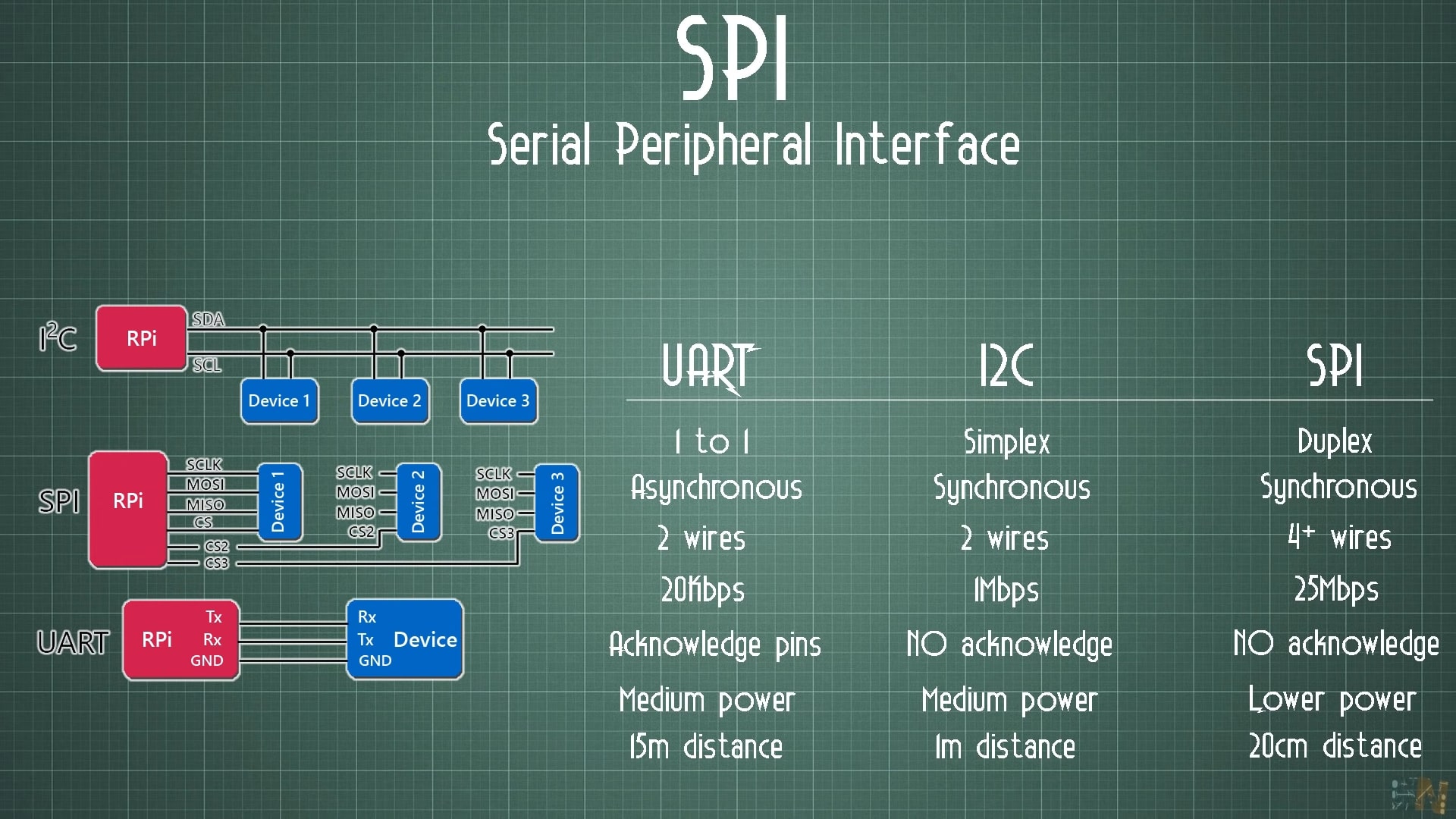
Diving more in I2C serial communication, I’ll be using my friends Adrián Torres Repo as a reference. I’ll also used Electronoob’s video that covers a better explanation on networking using I2C. I2C is a type of synchronous (needs a clock to send data) serial communication. What I like of this type communication is that you only need 4 pins to execute it and there is a variety of inputs and outputs that take advantage of it to communicate with the chosen MCU. The pins are VDD, GND, SDA (pin that sends the data) and SCL (Clock needed to send data).
The following screenshots are from the YouTube video of Electronoob’s. They help describe how the concept of the Master and slave devices work. The “MASTER” is the transmitter (TX) and the “SLAVES” are the receptors (RX). To have good communication as a requirement it’s really important that you give each “SLAVE” an address. I2C has a maximum quantity of 127 “SLAVES” in the BUS (main communication lines).
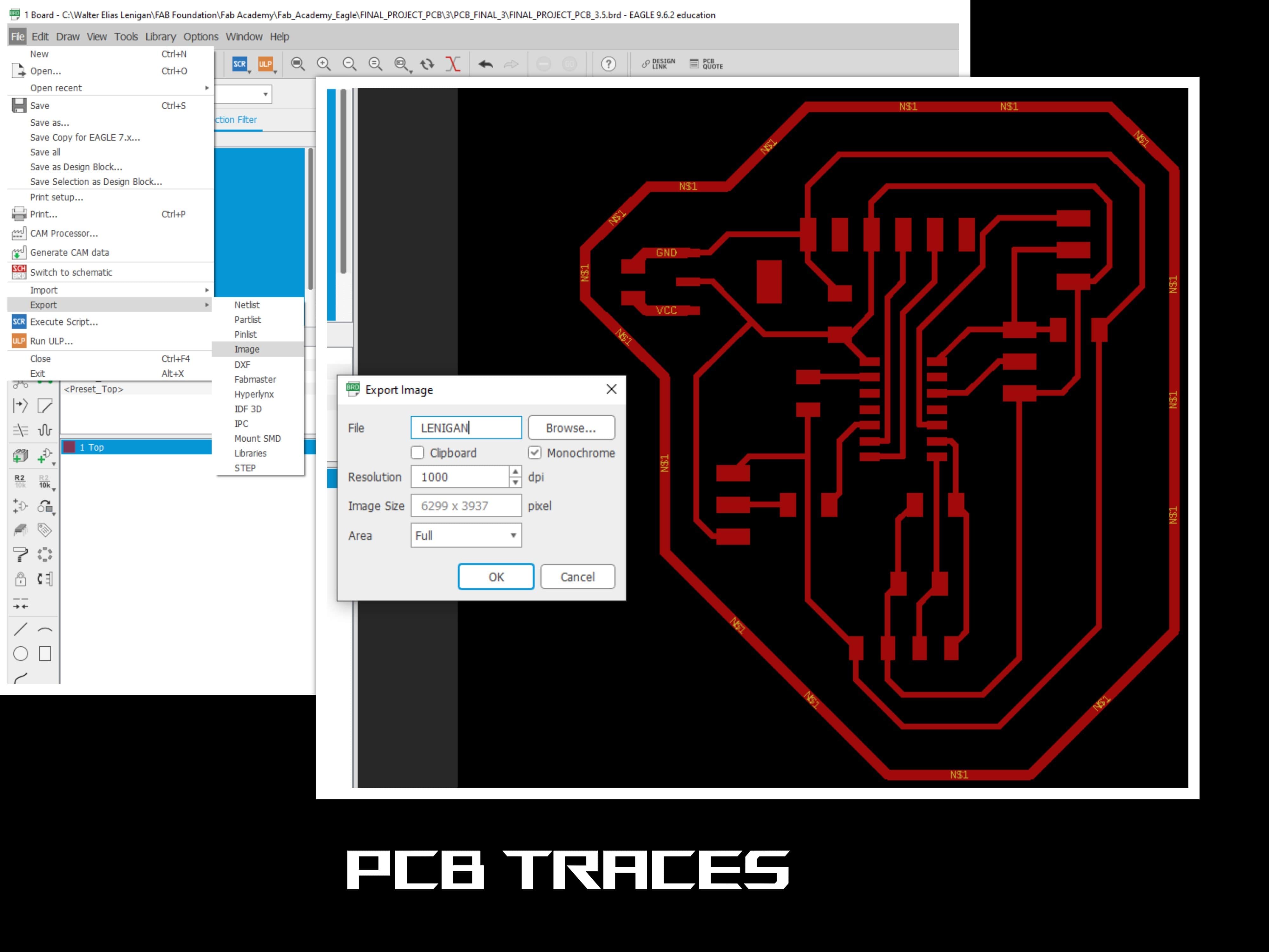
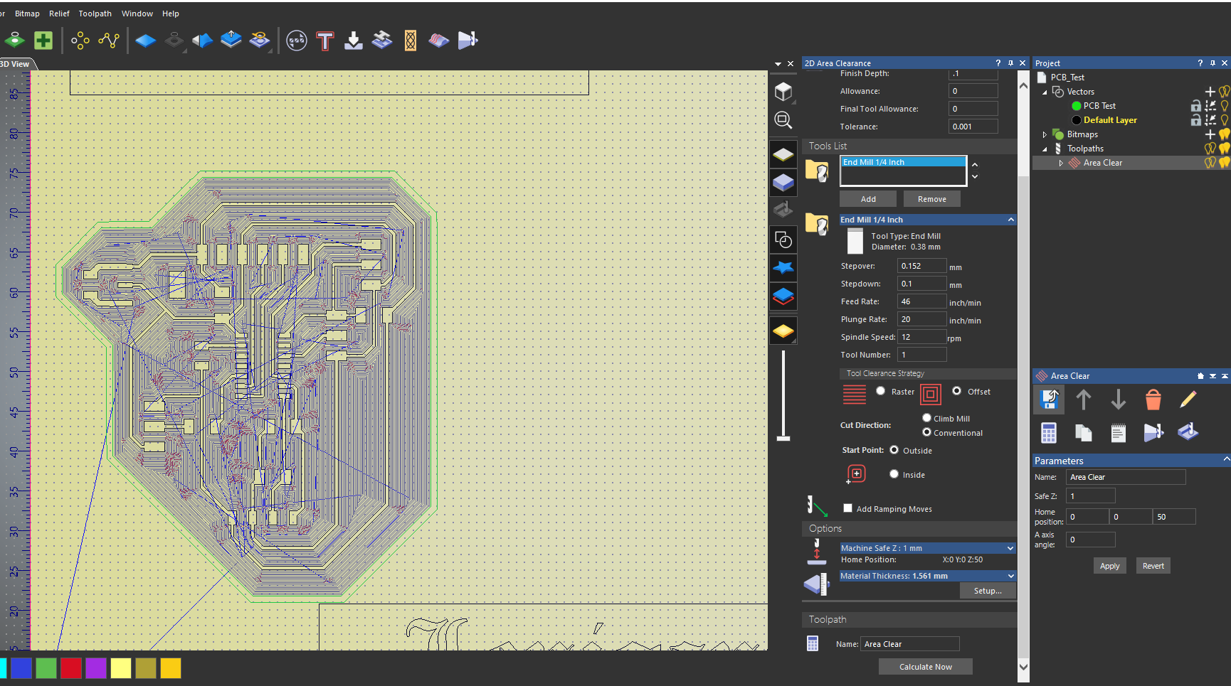
After exportin the monochrome picture I take the file in InkScape to use trace BitMap to generate vectors to import them in Carveco. I used a special end mill with the fallowing parameters:
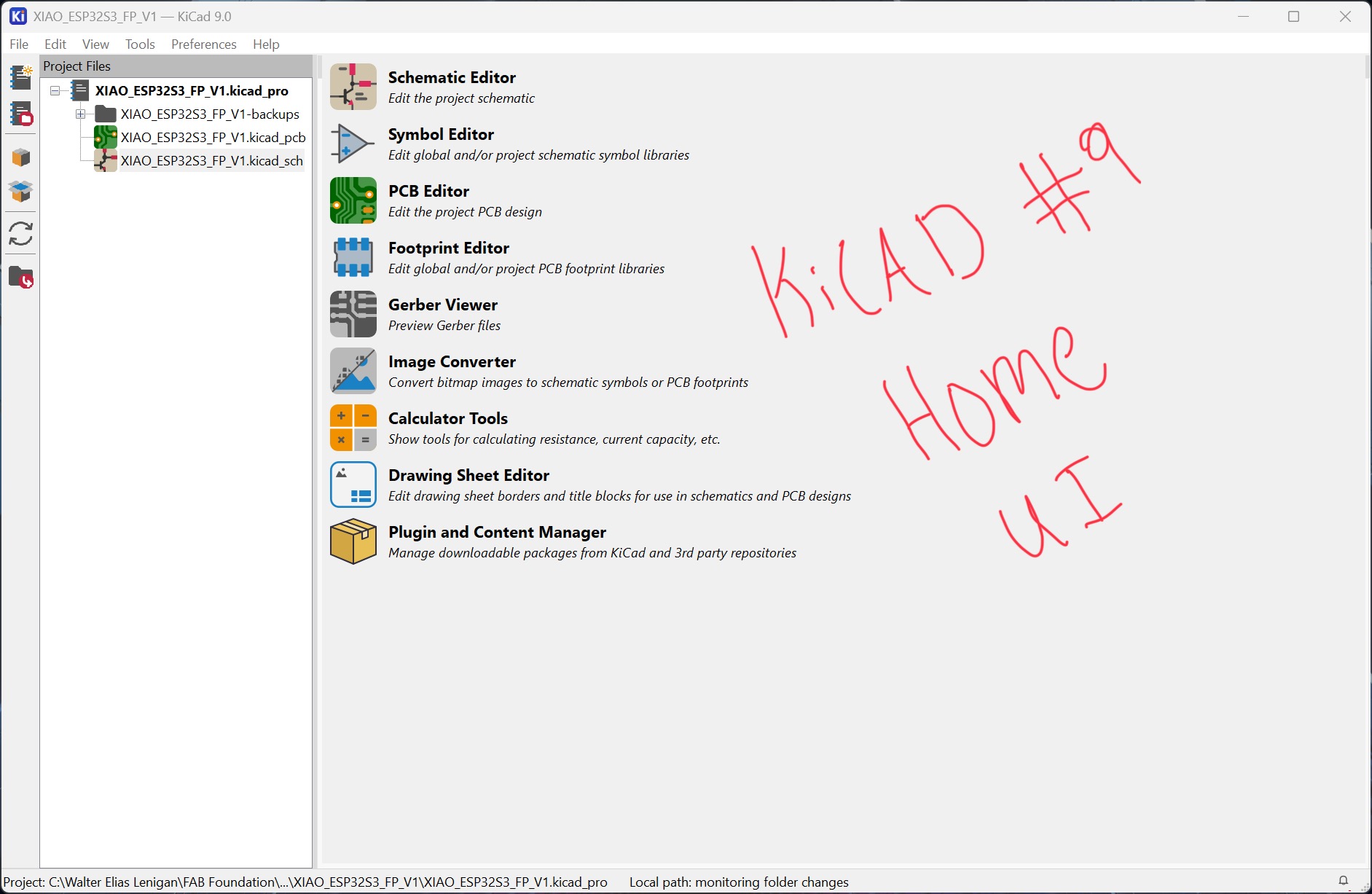
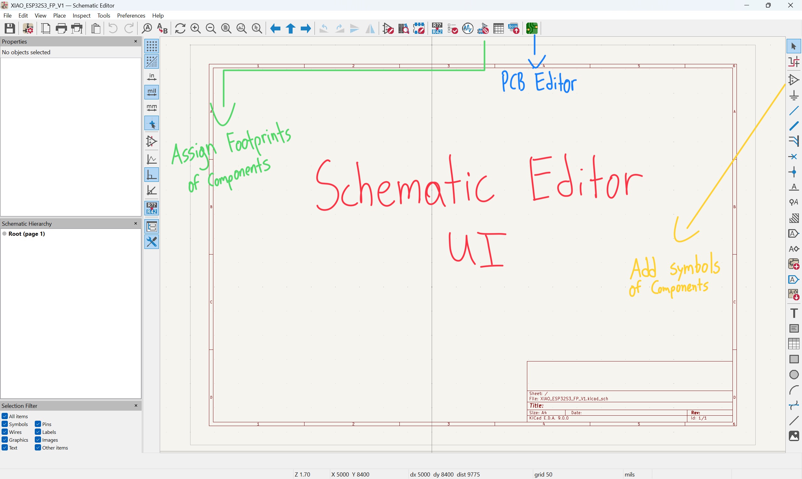
KiCAD is an open-source alternative for EDA (Electronics Design Automation) software. First you need to download the version of the software that matches the OS you’re using. After you’ll be greeted with the “Home” UI. Please see the following picture.
Now you need to download the FAB library so that you can work with components that you would see in the FAB inventory. The FAB KiCAD Library can be found in the FAB Cloud. The repo has detailed instruction on how to install the library. After adding the library, you can proceed creating a project file and opening the schematic editor. Please see the following picture.
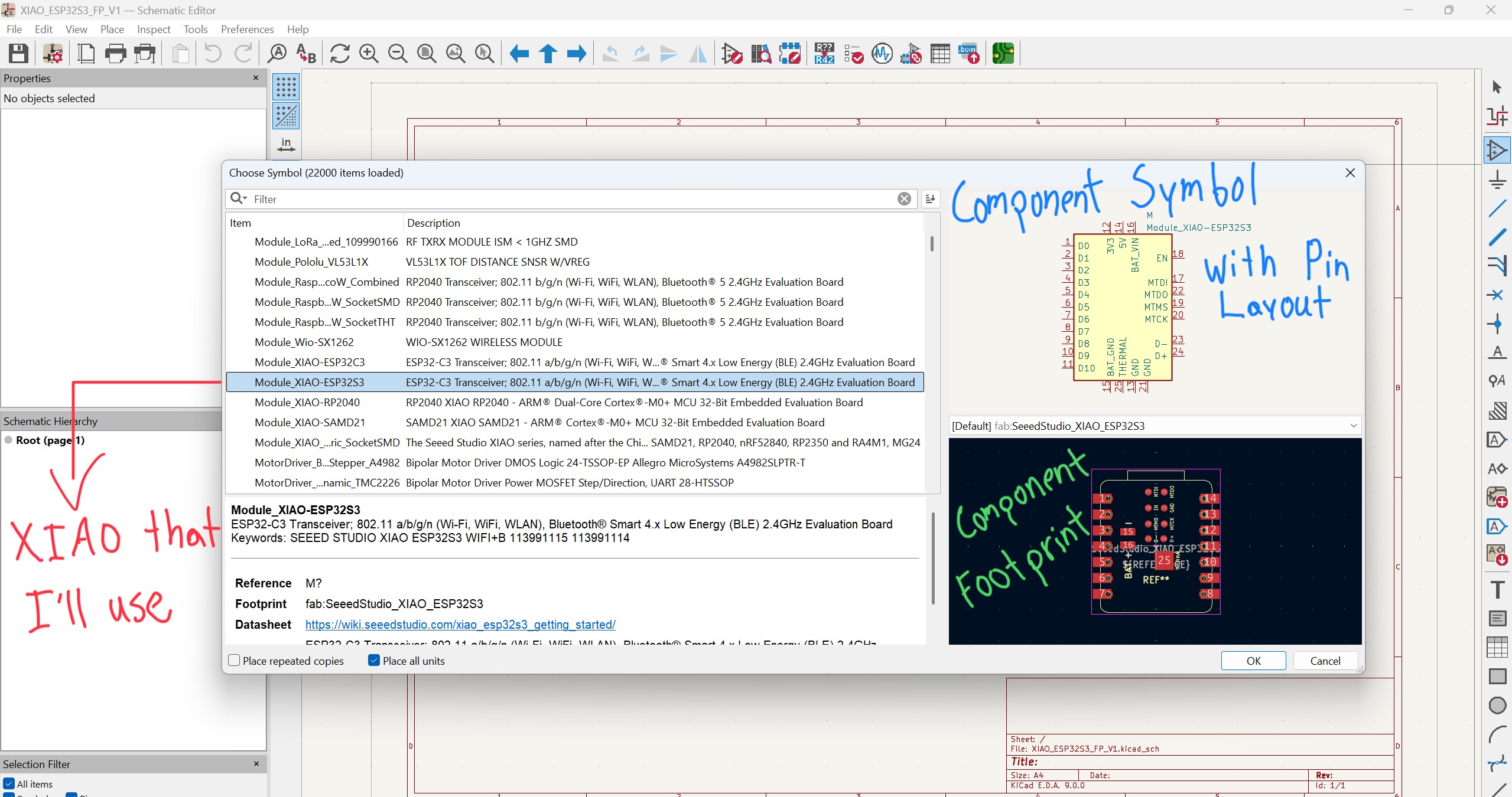
If you installed correctly the FAB library you should be able to see it by pressing the “Add Symbols” button that located on the top right tool bar. Scroll down and you should find the fab dropdown menu. I’ll add the XIAO I’ll be using to create my PCB around it.
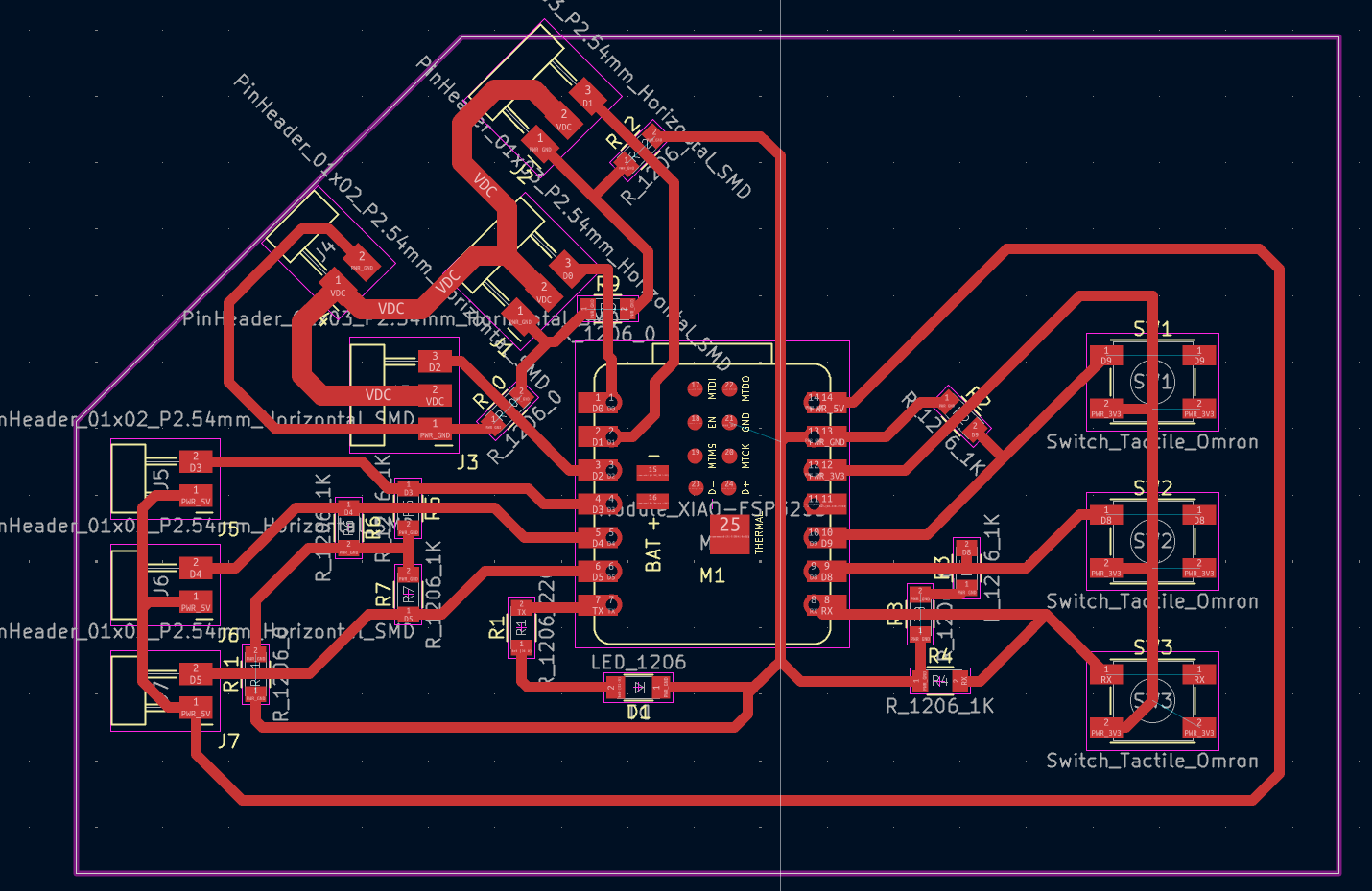
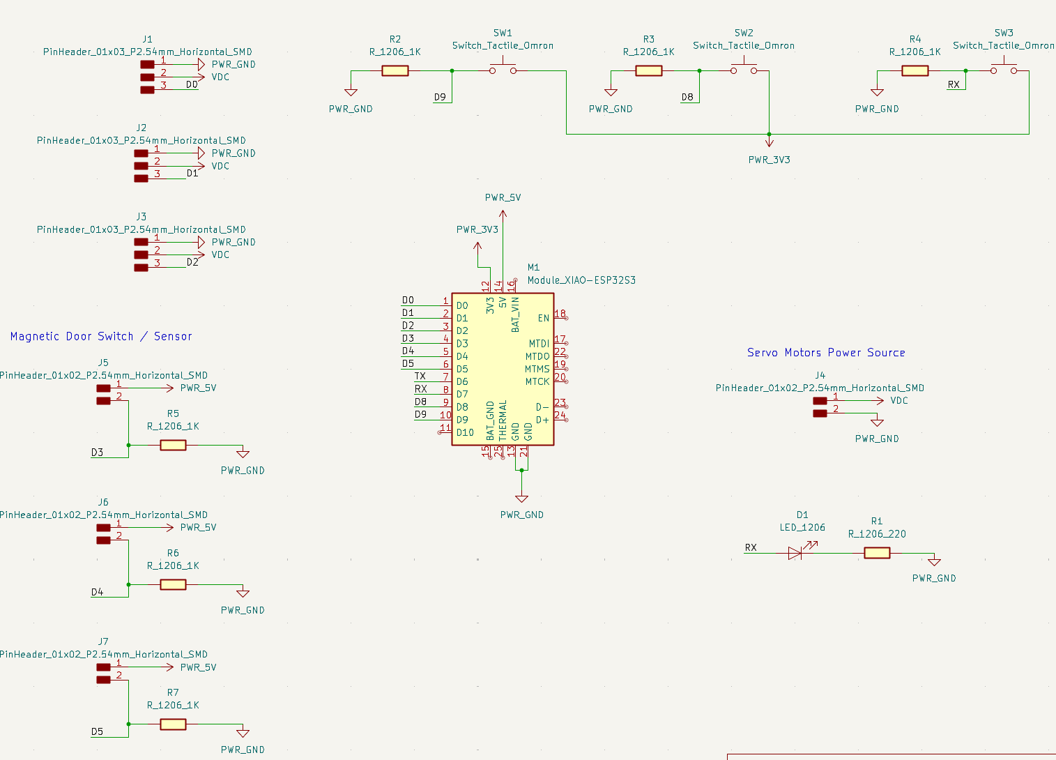
This PCB will be a prototype of my final project board. The schematic as 3 buttons that I will use just to trigger the servos to move. This will help test really fast if the servos are properly working. The PCB has 2 power sources that come from the XIAO ESP32S3 and the 3rd is an external power source (VDC) to run the servos. Servos add a lot of noise to the PCB circuit and this could disrupt the MCU coursing resets and more. Another reason is because the servos I’m using require more power to run properly. Just remember that for this to work the external power source and the MCU needs to have a common GORUND. The other jumpers are for easy connection of the 3 wires the servo needs to work and for the magnetic sensor / switch that will give me feedback (open / closed).
When the scholastic is done when can jump to the PCB editor of KiCAD. You’ll see that the UI changes and its empty (no components) unlike eagle when to switch to their version of the PCB editor. Please see the following picture to have a better understanding.
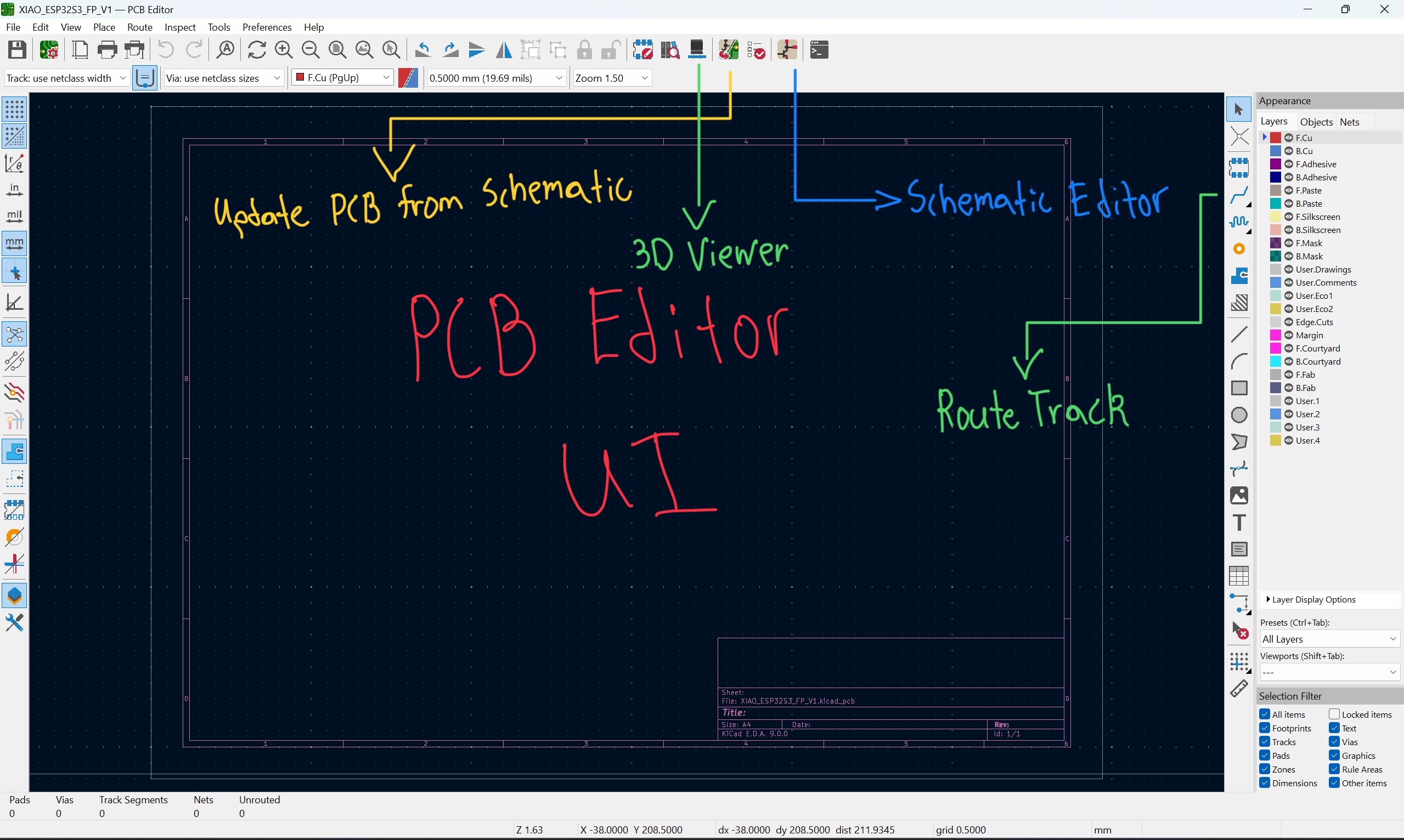
The final step is to move the components and route them maintaining the design to work just in one layer and if you have no other options you could jump to a two-faced PCB. Remember that the 0Ω resistors are you best friends. They work like “jumper cables” in a SMD platformer. KiCAD also gives use the option to render the board that we just designed.