Assigment #4
electronic production
The 4th assignment of the fabacademy it’s electronic production.
We have to use a cnc milling machine to produce an ISP programmer.
The first thing to do it’s to mill some FR1 sheets to test the design rules of the circuit we’ll design.
1 – export the files for milling
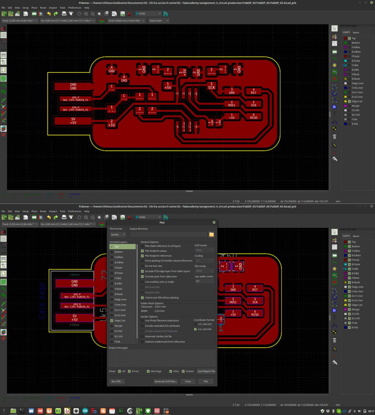
After a little research about what former FabAcademy studens did to achieve this goal, I decided to go for a pcb designed by a former Fab Academy student named Axel Cornu . This is a very nice design that improves some aspects of Brian’s design of the FabISP, and there’s a great intraduction featuring prof. Farnsworth, that’s more than enough for me... From Axel’s page I downloaded the Eagle version of the circuit and opened it on Kicad. From kicad I exported a GRBR file of the design, making sure to export only the top layer (containing the paths) and the Edge-cut layer, containing the path needed to mill the cutout of the pcb.
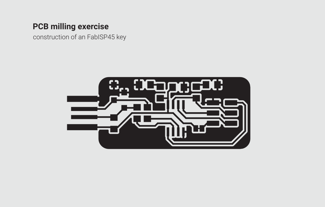
The circuit will be made of the following parts
1x – ATTINY45 microcontroller
1x – 100 nf capacitor
2x – 47 Ohm resistors
2x – 150 Ohm resistors
1x – 1,5 KOhm resistors
2x – 3,3 V zeeners
2x – LEDs
1x – 3x2 pin connector
3 – turn the geometry into a milling path
2 – generating milling paths and gcode
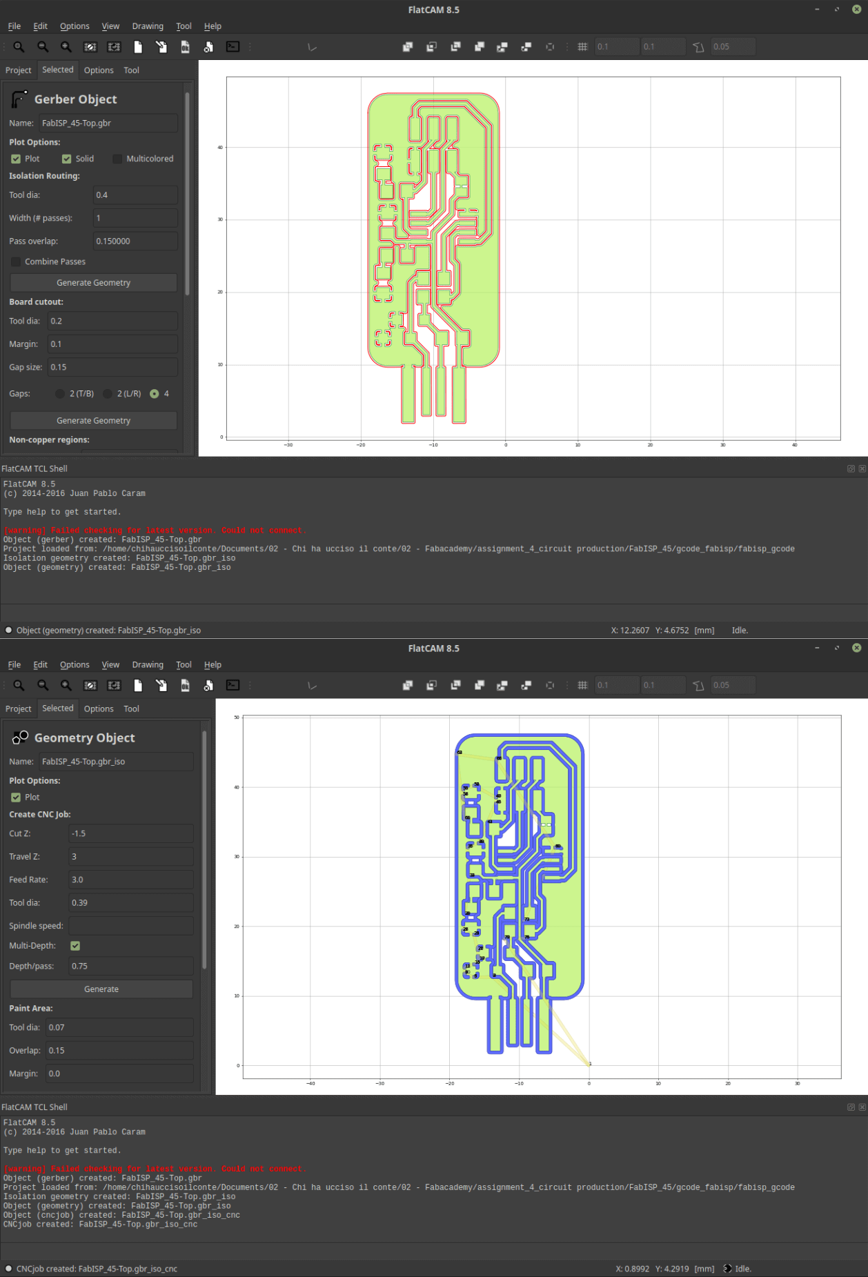
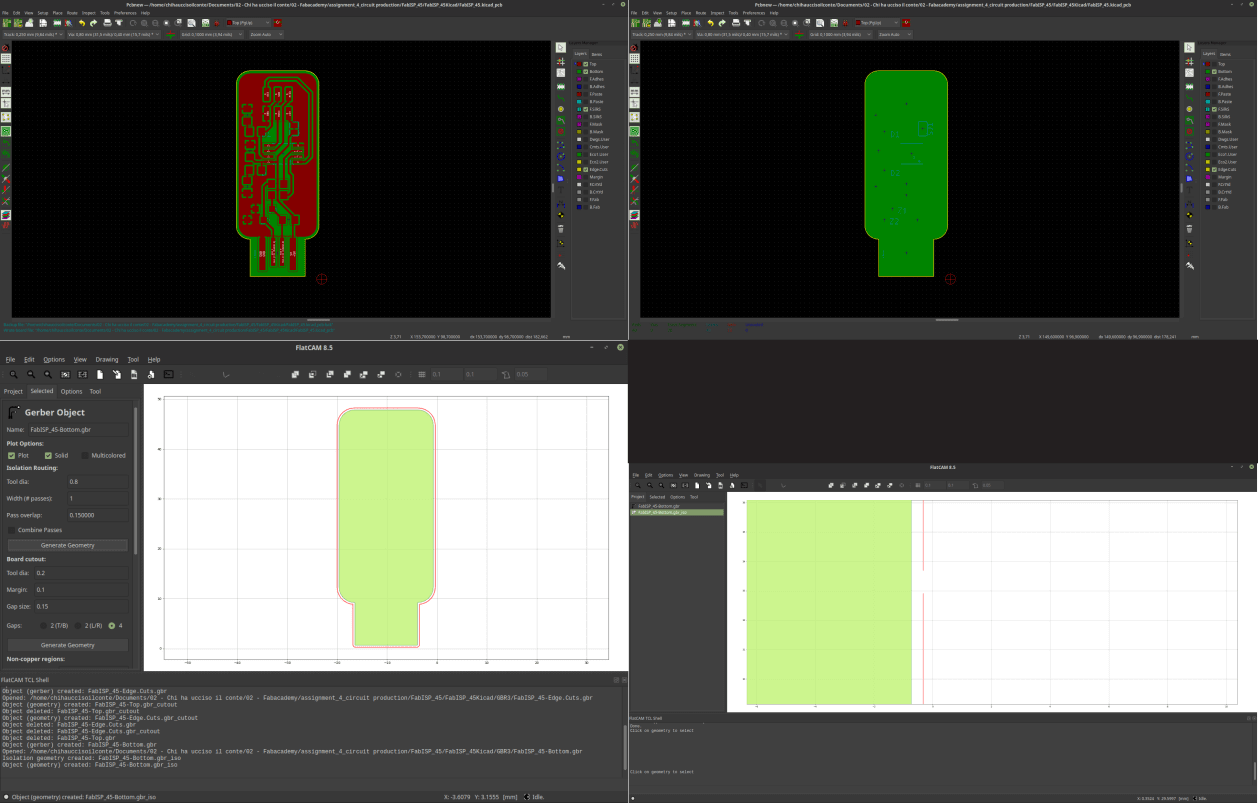
To generate the gcode I decded to use a software called FlatCAM.
Flatcam it’s an open source gcode generator designed by Juan Pablo Caram. Flatcam allows you to import GBR and SVG files and create path around them.
The first thing to do it’s to import your gerber files and create a path around it, in my case I’m going to start with the paths of the traces.
The software needs to know the diameter of your tool (in my case 0.4), the feed you want to mill your pcb at (I went for 30 mm per minute).
This process happens through 3 main steps:
1 – import the gerber file
2 – create a geometry aorund it
3 – turn the geometry into a milling path
Once the path for the traces was done I switched to the cutout, but I noticed that, if you use the “board cut” function, Flatcam creates a rectangle that inscribes the form of your Gerber in stead of cutting your shape, which is bad since I need my pcb to be USB-shaped…
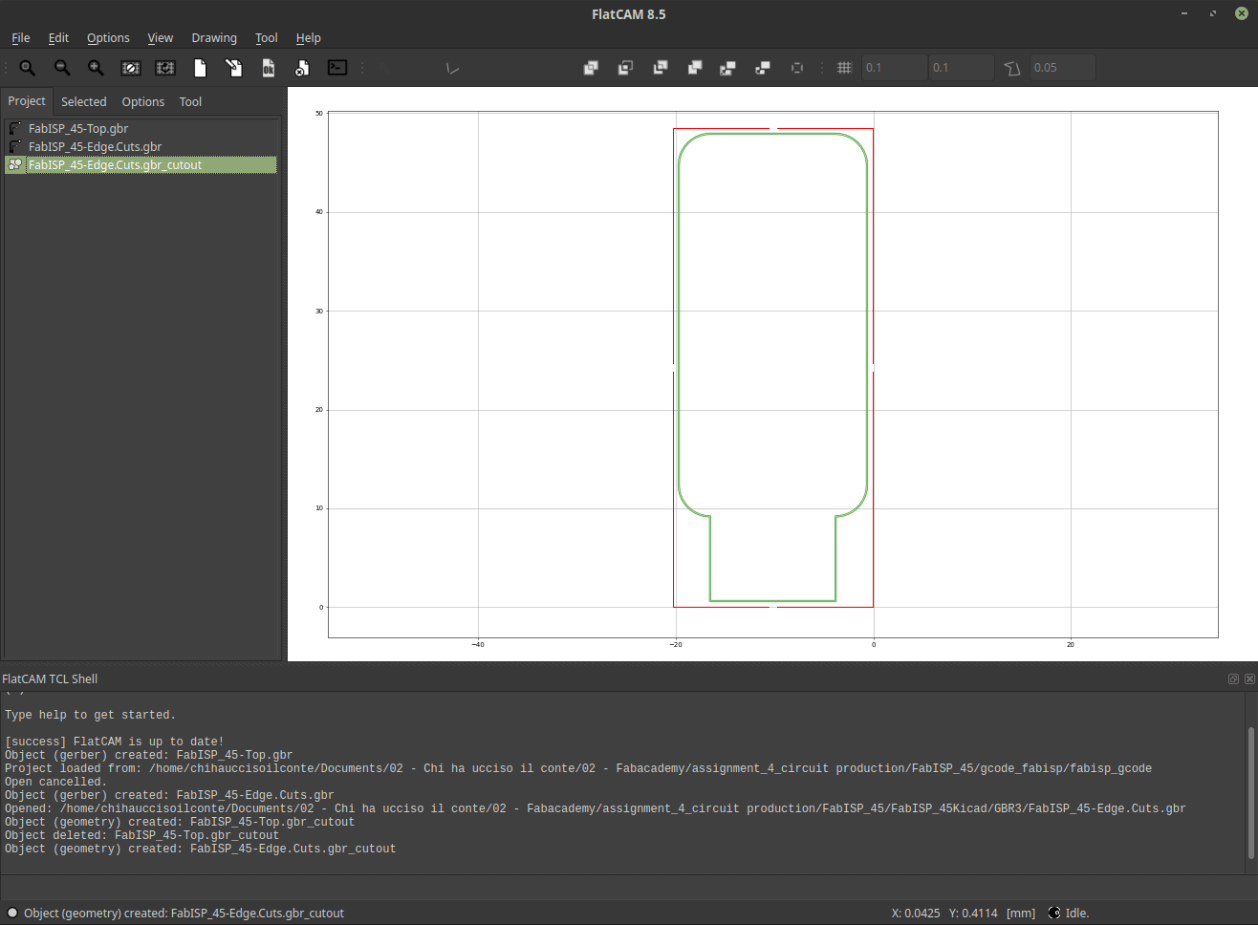
I had to find my way around it, so I did it by following this tutorial.
To start I moved back to KiCAD and created a filling in the bottom layer. In this way I’ll make a gerber that has the same shape as the piece I’ll be cutting.
Then I import it back to Flatcam, and I treat it like a circuit trace, but I sat bigger bit (0.8 mm) and a deeper cut (1.5 mm). In this way the software is able to generate a path that goes around the shape I need.
To be extra sure about not doing a mess I created manually some tabs by using some commands inside the “edit geometry” function of Flatcam.
 Once this is done I exported the two gcodes and moved to the machine!
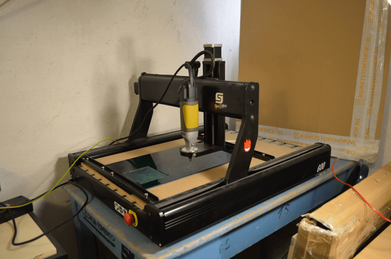
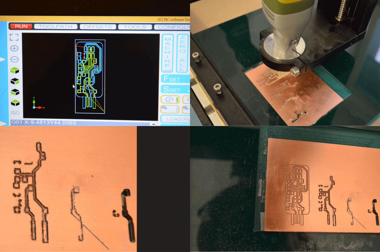
3 – Milling the pcb
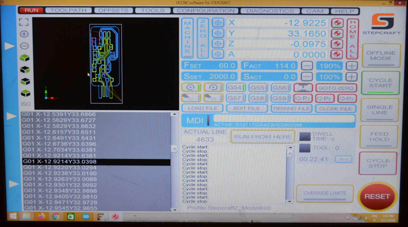
Now that I’ve got my gcodes it’s time to approach the machine. The machine I’ll be using it’s a Stepcraft 2/600 Black Edition. The black edition of the Stepcraft series it’s upgraded with more precise stepper motors that allows the users to make precision works like PCB milling. The spindle I’ll be using it’s a Proxon. The speed of the rotation will be manually controlled through a little knob on the spindle.
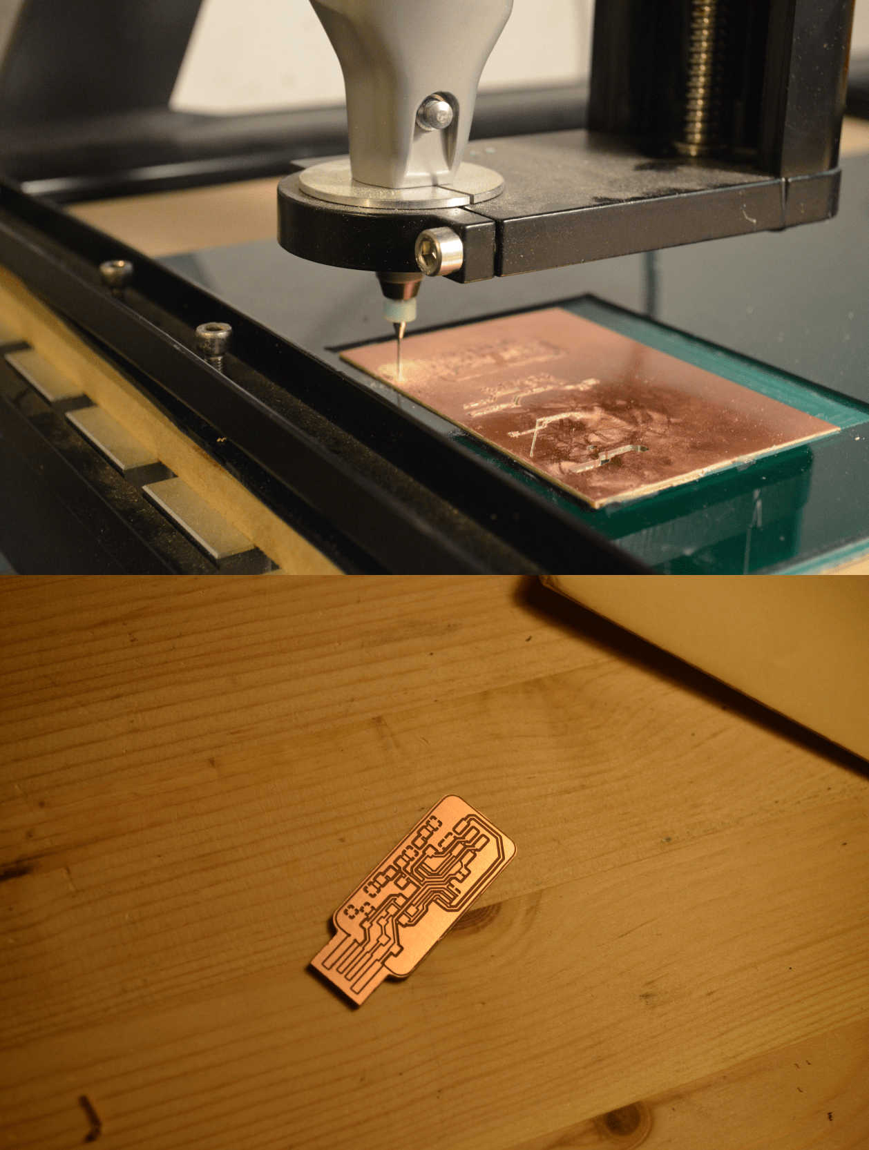
The first thing I did was to mill a simple square on a polycarbonate sheet. In this way I’ll be sure that the working plate and the movements of the machine are exactly parallel. Then I used some double sided tape to stick my FR material to the panel. Once this was done I opened UCCNC, which is the driver of the machine. Through this software I can drive the movements of the machine and set the origin of my milling work. To do this I simply move the tool to the position that I want to use (in my case the right-lower part of the FR material) and click on “zero all”. To set the z axis, which is the most delicate task, I did just like Neil told us: I placed the spindle a little above the position of the plate, and then I loose a little the grip so that I could accompany the bit down until it touches the surface of the material, then I secured it and sat that as the origin for the Z axis.
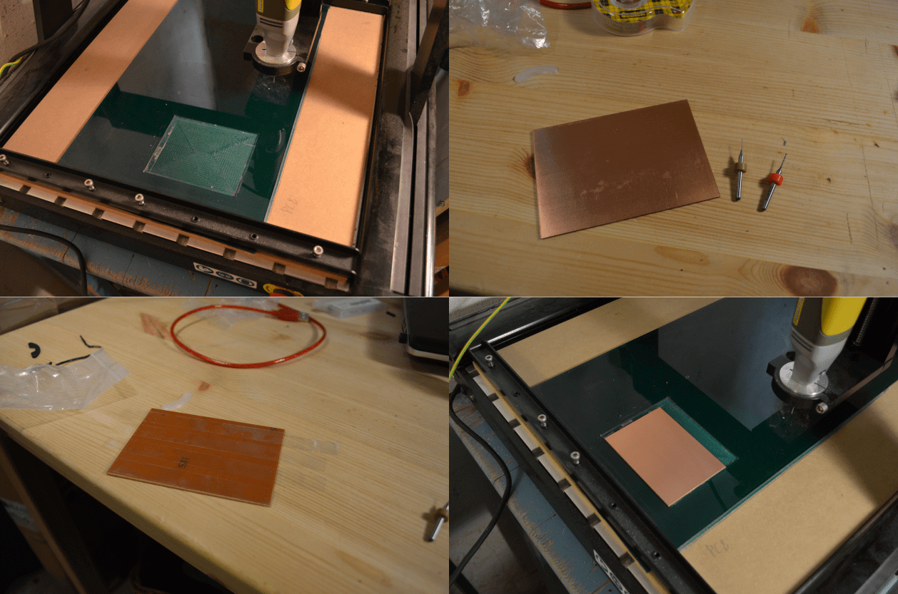
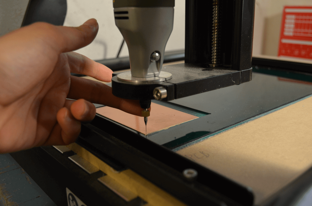
The machine started to move, but the first attempts where quite bad… I first made a mistake in the CAM, where I set as cut dept “1,5” in stead of “0.15”. this turned into a disaster, I made a trace shaped hole in my pcb… But with my surprise the bit didn’t break, so I corrected the gcode and re sent it to the machine, but the bit was actually really bad, and the cut was very bad, so, failure n° 3. I changed the bit and sent the job once more, and this time it went finally well. Then I changed the bit (0.8) to work on the cutout, and fortunately this wend well at the first attempt. I had my PCB finalli in my hands!
4 – Solder on the PCB
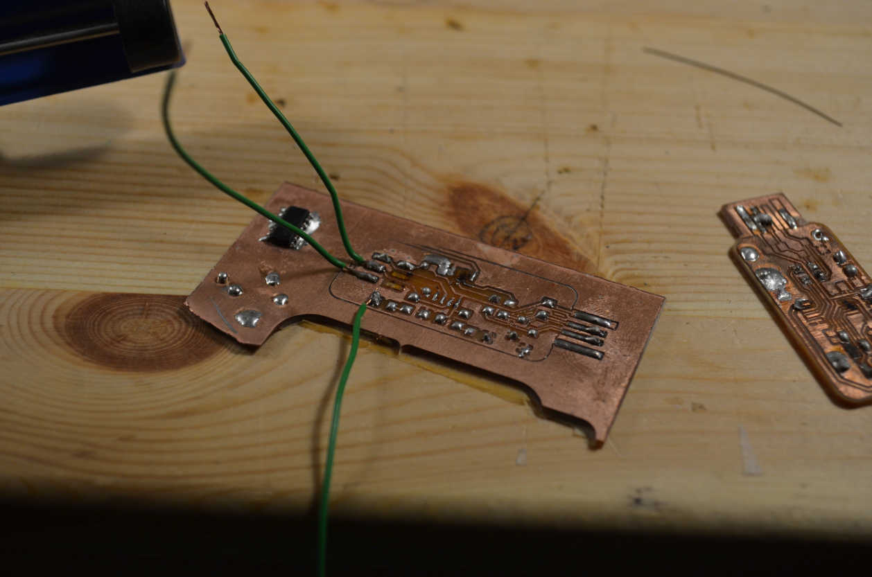
I was super happy with my PCB milling session, and I finally moved to the soldering phase, where I could finally put all the components together and start to make my pcb working. I was very excited, but as soon as I touched the surface of the pcb with my soldering iron, the track charred immediately and my PCB was no longer usable… After this traumatic experience I just started to put tin on the other parts to get a little more used to the practice, but I think I made quite a mess. I’m going to make another board, and then I’ll try to solder the components avoiding direct touch between the iron and the pcb
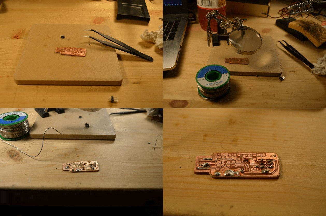
5 – Solder on the PCB 2 – the copper battlefield
Once I milled again the PCB I was quite scared to approach it again, and therefore I decided to use the old PCB as well as some failed attempts to practice my soldering skills.
I also followed some tutorials to get precise instructions about how this is done, the best I can recommend is definitely this one by the mighty Collin Cunningham. The tutorial it’s very well made, the only thing that I feel like adding to it is that since we are not putting solder mask on our PCBs we’ll need to be extra careful not to ruin our board (like I did before…), and the use of solder paste really helped a lot in the process. Beside this, I milled two more boards and placed almost all the parts on it, but as soon as I touched the pin connectors… ...BAM! The connectors went away, bringing a consistent part of the traces with them. This was truly frustrating, and It left me no choice but to throw away the board and start over again (what the hell...).
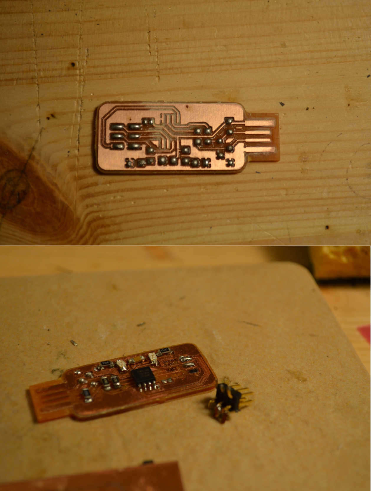
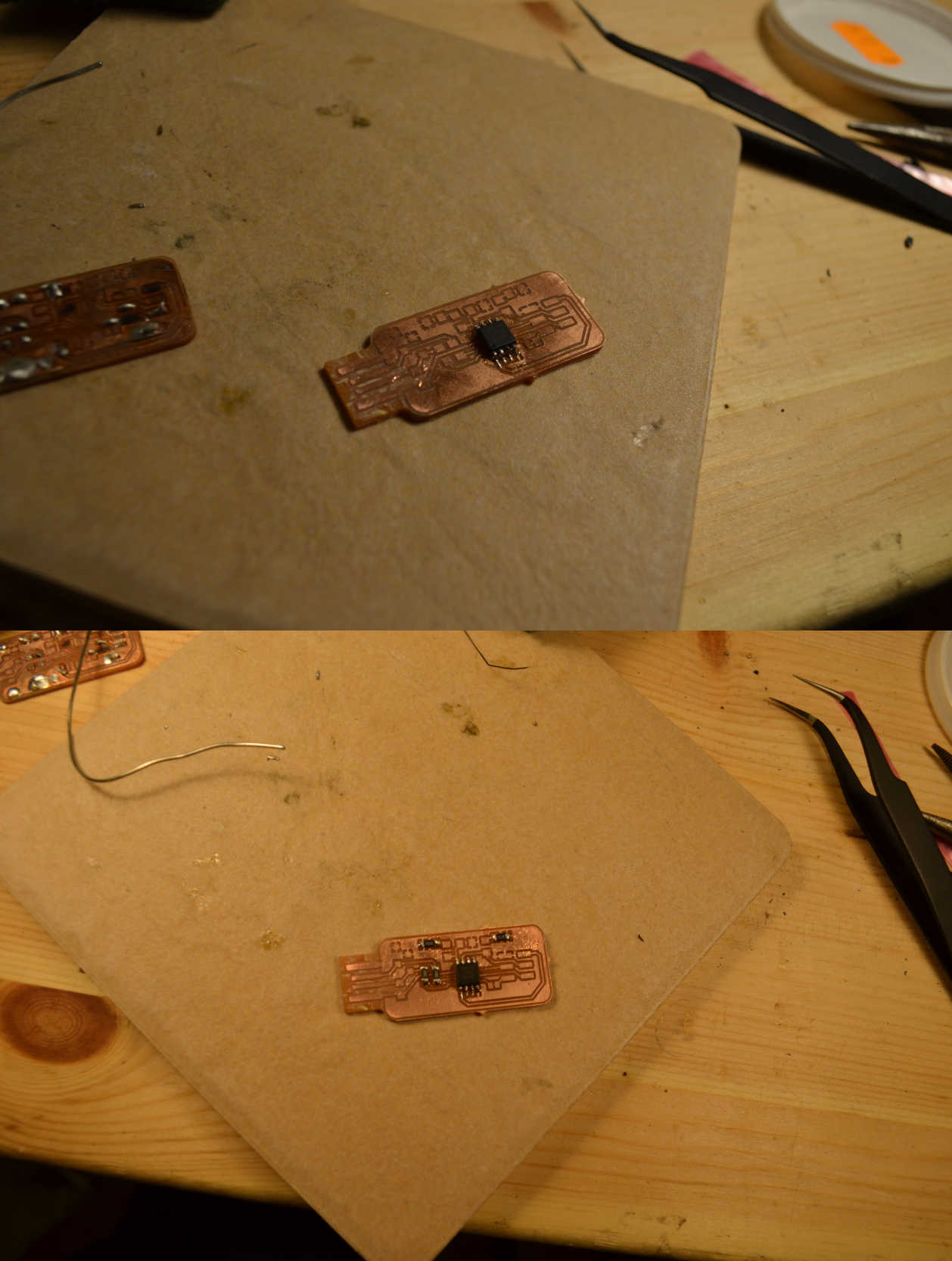
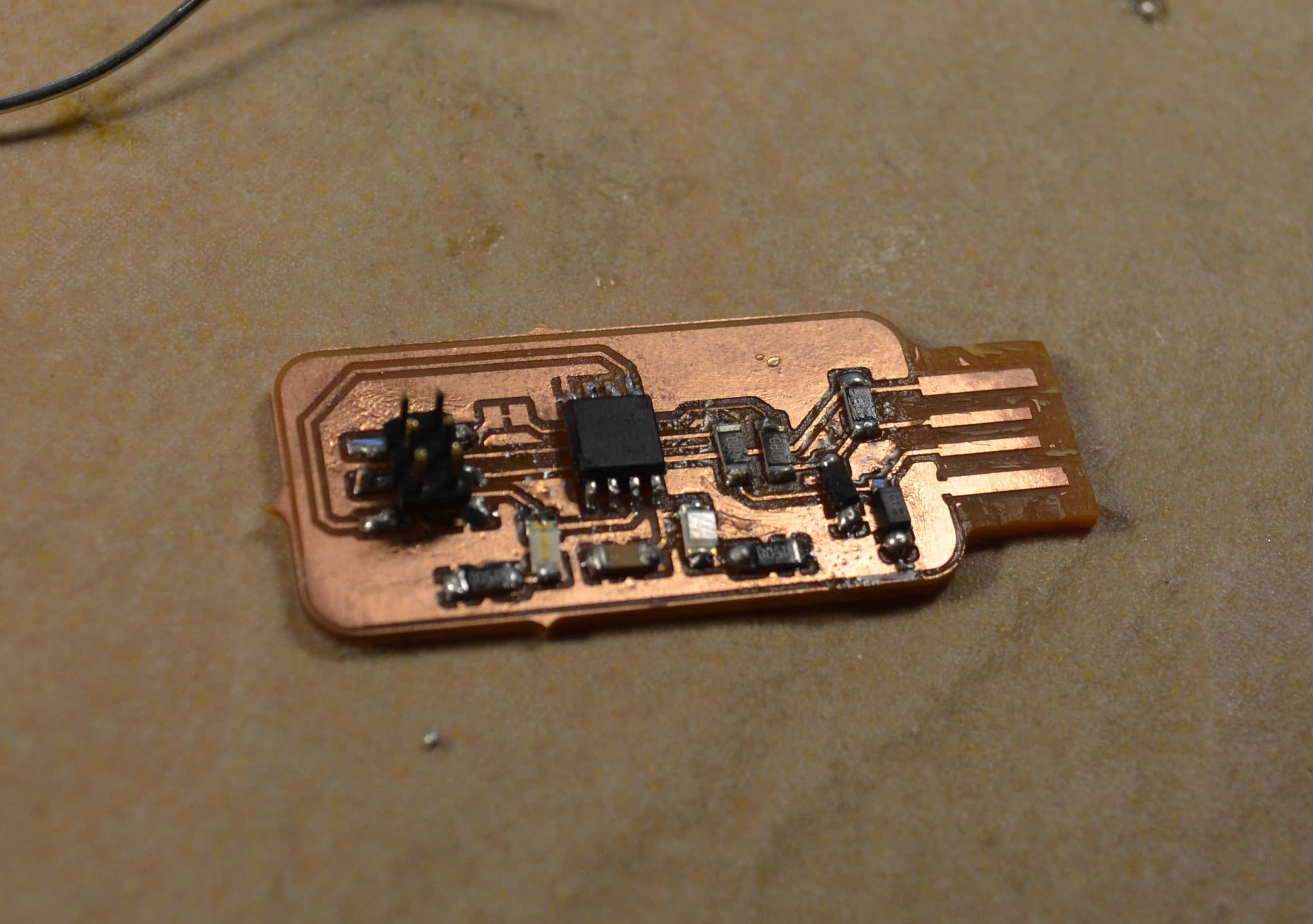
I did my best to keep the moral up and solder everything again, this time fortunately everything went fine, here is the result
6 – flashing the ISP programmer
To flash the isp programmer I used an Arduino, because I don’t have an already working isp programmer. I used this tutorial to do it
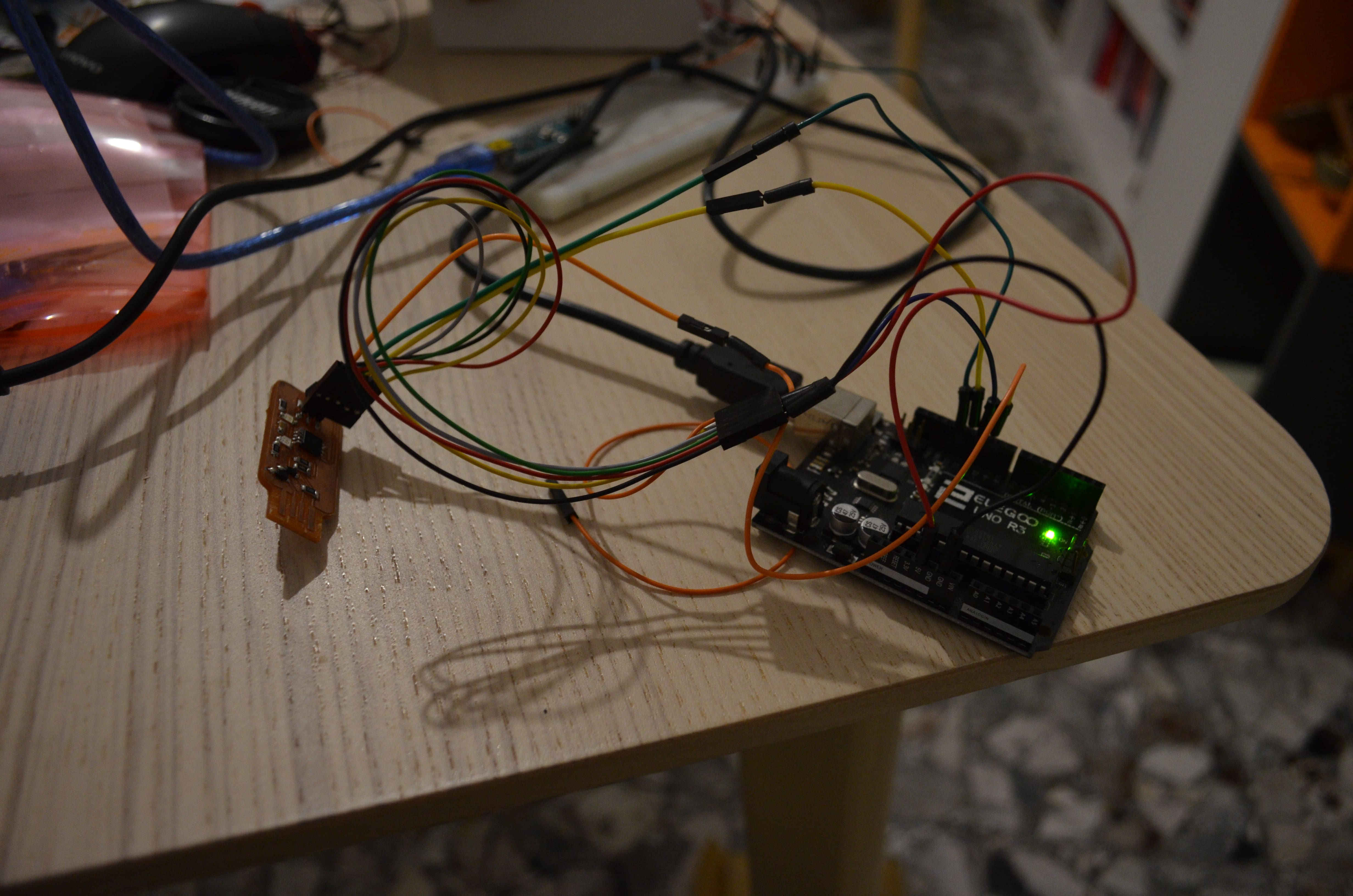
once the setup of the arduino was done I had to edit the makefile of the firmware, changing putting the USB port of the Arduino and the attiny45 as a controller.
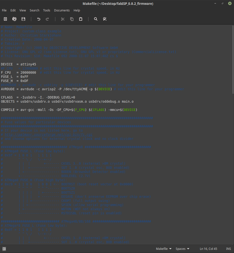
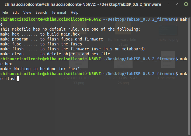
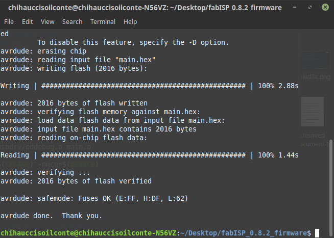
Once this operation was done I just went through this tutorial opened the folder on my terminal and typed: Make hex to generate a hex file (althought the terminal misteriously said that "nothing to be done for hex") , and then Make flash o finally flash the ISP programmer
source files
Here are all the source files for the Electronic production assignment:
1 – KiCAD file for the FabISP 45 Key
2 – GBR + SVG files for the FabISP 45 Key