Week 18: Project development
INDEX
- The plan A
- The plan B
- introduction
- what will it do?
- whats skill will be involved inthe process
- drafts and sketches
- first concept
- CAD
- One wire diagram
- ECAD
- CAM and ECAD Bloppers
- Time Strategy
- Final project
- links and references
The Plan A
The smart fab
The queretaro Fablab were i work at works inside an university campus and people from diferent backgrounds have access to the machines in our laboratory. It is called the printing laboratory i'ts a place where Students, Teachers, Former students and Administrative staff can make their personal projects and educative props and only the costs of the materials are counted we have a recorded history of the uses per machine on an excel spreadsheet where we input the internal ID for each person as well as Name, Area, Machine used, and Material Cost.
but it is quite tedious for one person to keep track of all the uses on the machines so in order to improve this my final project aims to automaticly log the use per machine registering it to the internal ID the university gave to each user we all have one ID badge where is printed a unique barcode and have a rfID chip as well.
id'like to avoid creating a new database for this project so instead i'll have to learn to use the mySQL internal database that already exist with the personal info for every user registered on campus
the goal is to atatch a magnetic 3 phase contactor controlled by an atTiny digital output and a relay to feed the magnetic contactor coil
so, in this page my goal is to post my project management scheme in steps to follow
- 1.-Create a sketch of the general design
- 2.-Create a bill of materials to use
- 3.-Design a good housing for the electronics and the wiring
- 4.-Program an attiny44
- 5.-Make a pcb with a push button and a LED and make it blink with the atTiny whe the button is pressed
- 6.-Make a relay PCB with some headers and use it to turn a light bulb using the atTiny button PCB
- 7.-Attatch a rfID shield to the atTiny board and read some ID's to get the data out of them
- 8.-Control the light bulb using the rfID data without the data base just granting acces with the data of the code
- 9.-Integrate the mySQL database locally on a pc attached to the atTiny to read data from the database and control the light bulb
- 10.-attatch a wifi shield to the atTiny board to read the mySQL data base from a locally served host with a static IP
for the first part i will be using handmade sketches i've drawn over the course of my fabacademy experience
this one is hosted on my flickr page from the first week this is just a doodle i did about the objective of the project
The plan B
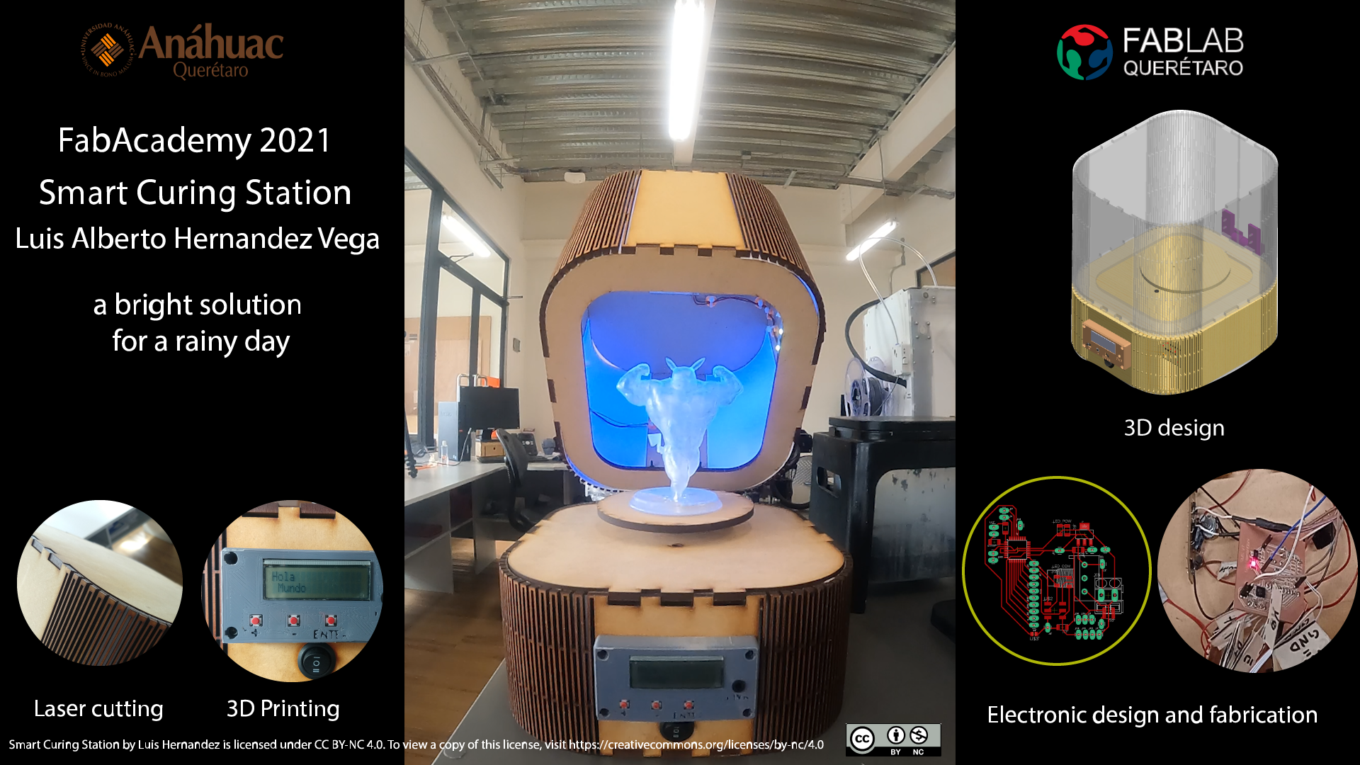
The Smart Curing Station
Introduction
what will it do?
so in this Plan B project i intended to use as much fabrication methods as i could.
what skills will be involved in the process?
drafts and sketches
of course i've being doodling arround the idea thinking what i may need for making this project
This is the general idea of what needs to be
as well as a sketch of an android app that this will need (i tought it could be really fun to teach in a classroom).
this is the general idea of the app
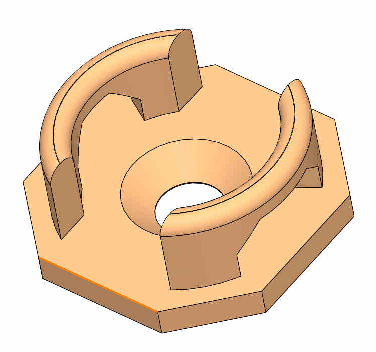
Digital concept
this is just an isometric view of the solidworks model
From the list above i'll try my best to answer this questions
what tasks have been completed, and what tasks remain?
what has worked? and what hasn't?
what questions need to be answered?
what will happen when?
what have i learned?
also i'll explain a little bit about my little contribution to COVID-19 Response. Designing some splitters, reusable ventilator valves, face shields, and intubator shields. HERE
i'll drop all of the links at the bottom as usual.
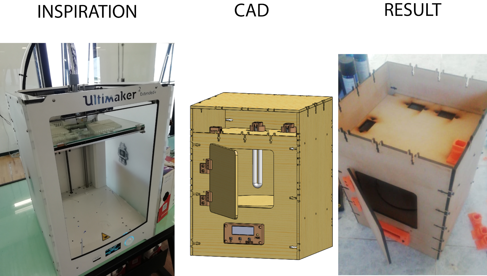
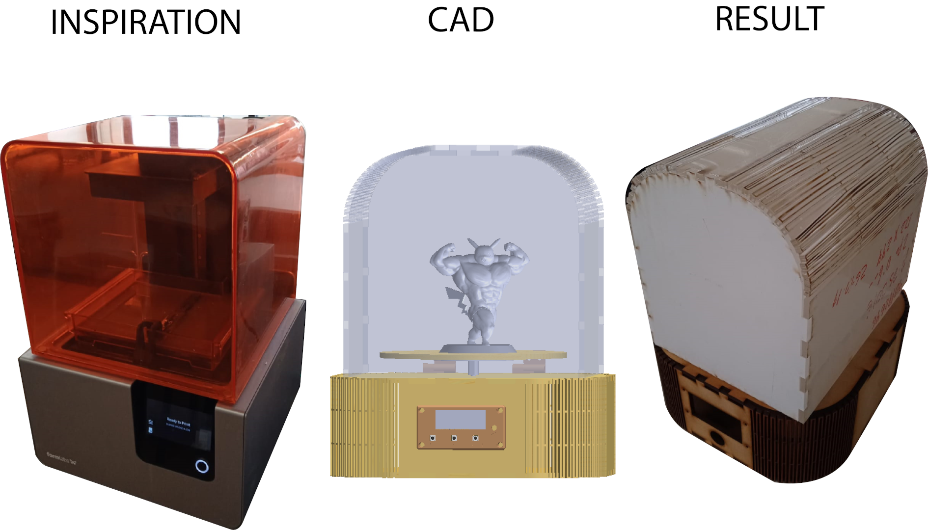
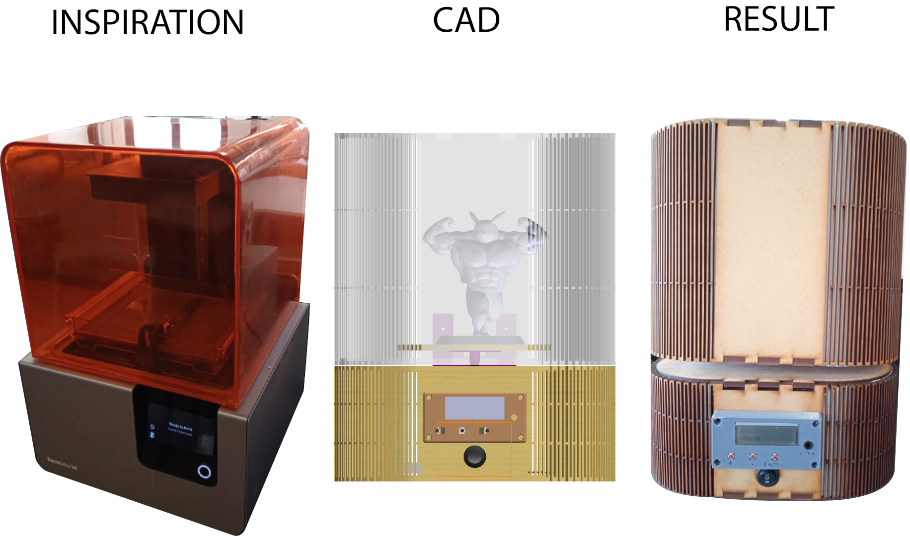
CAD
Here i'll drop all of the info about all of my CAD files on my diferent versions.
For my 3d modeler CAD parametric software i use Solidworks
as for the CAM for the 3d printer i used Ultimaker's CURA
and for the laser processing software i use LaserCA
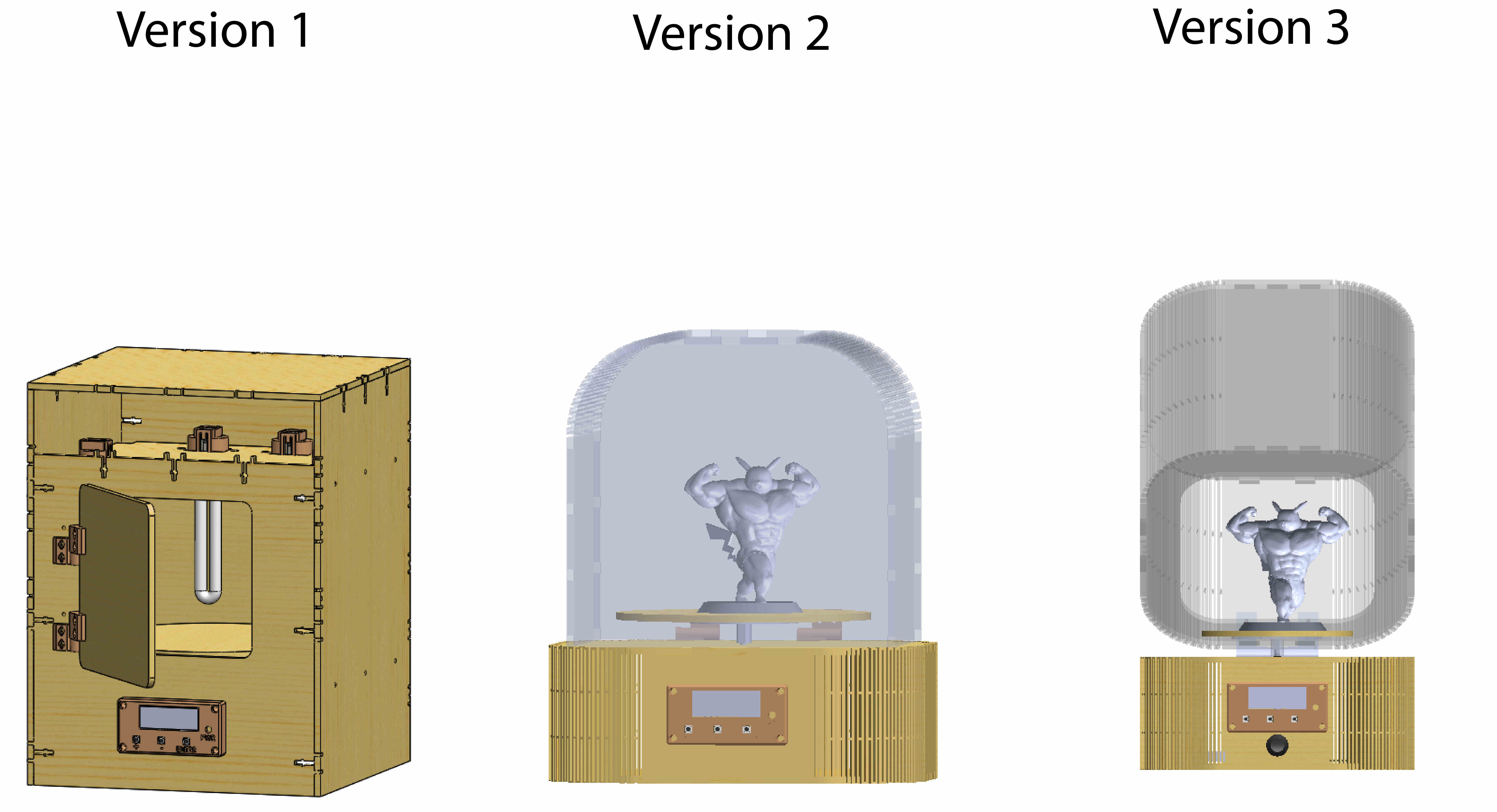
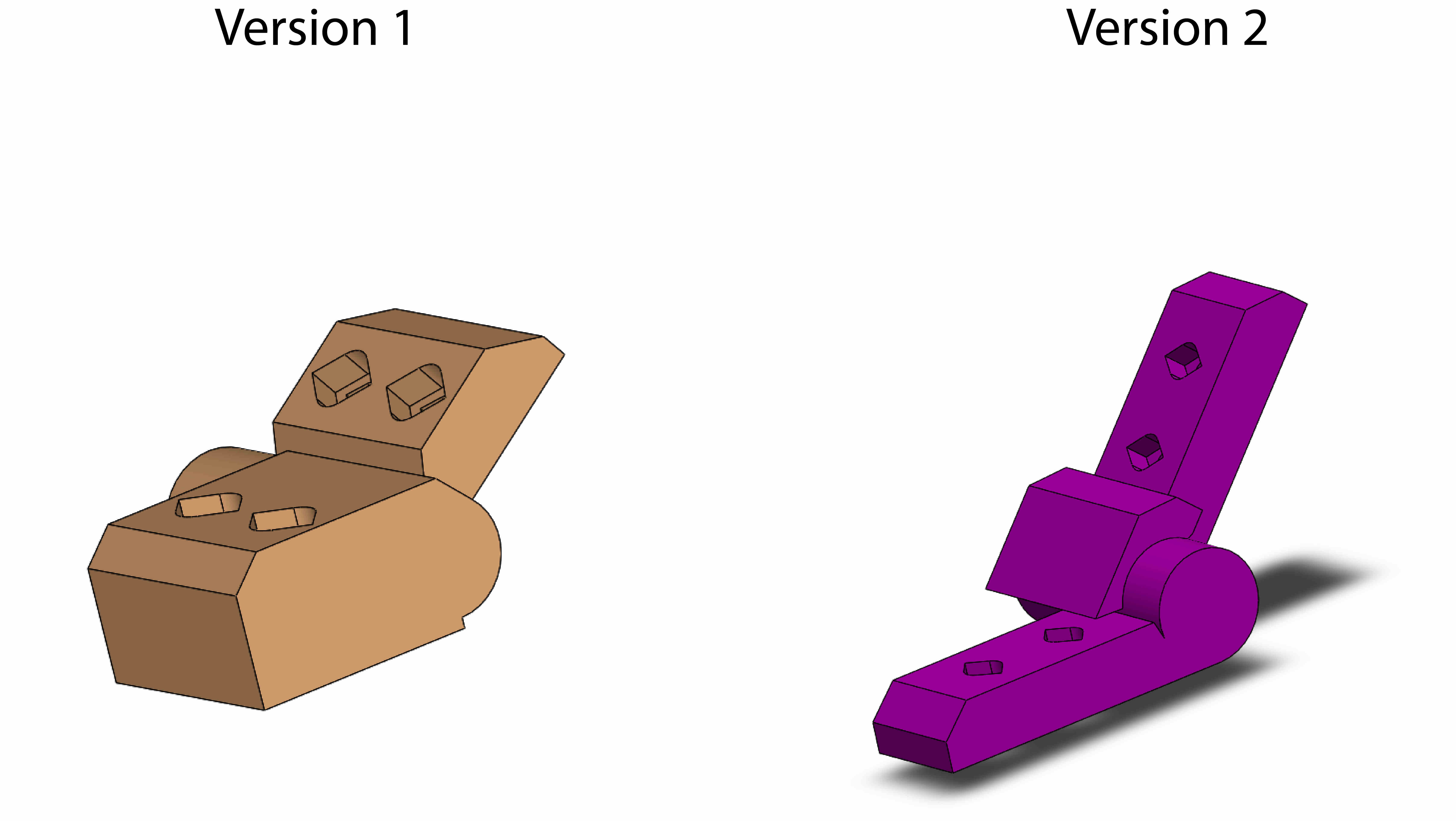
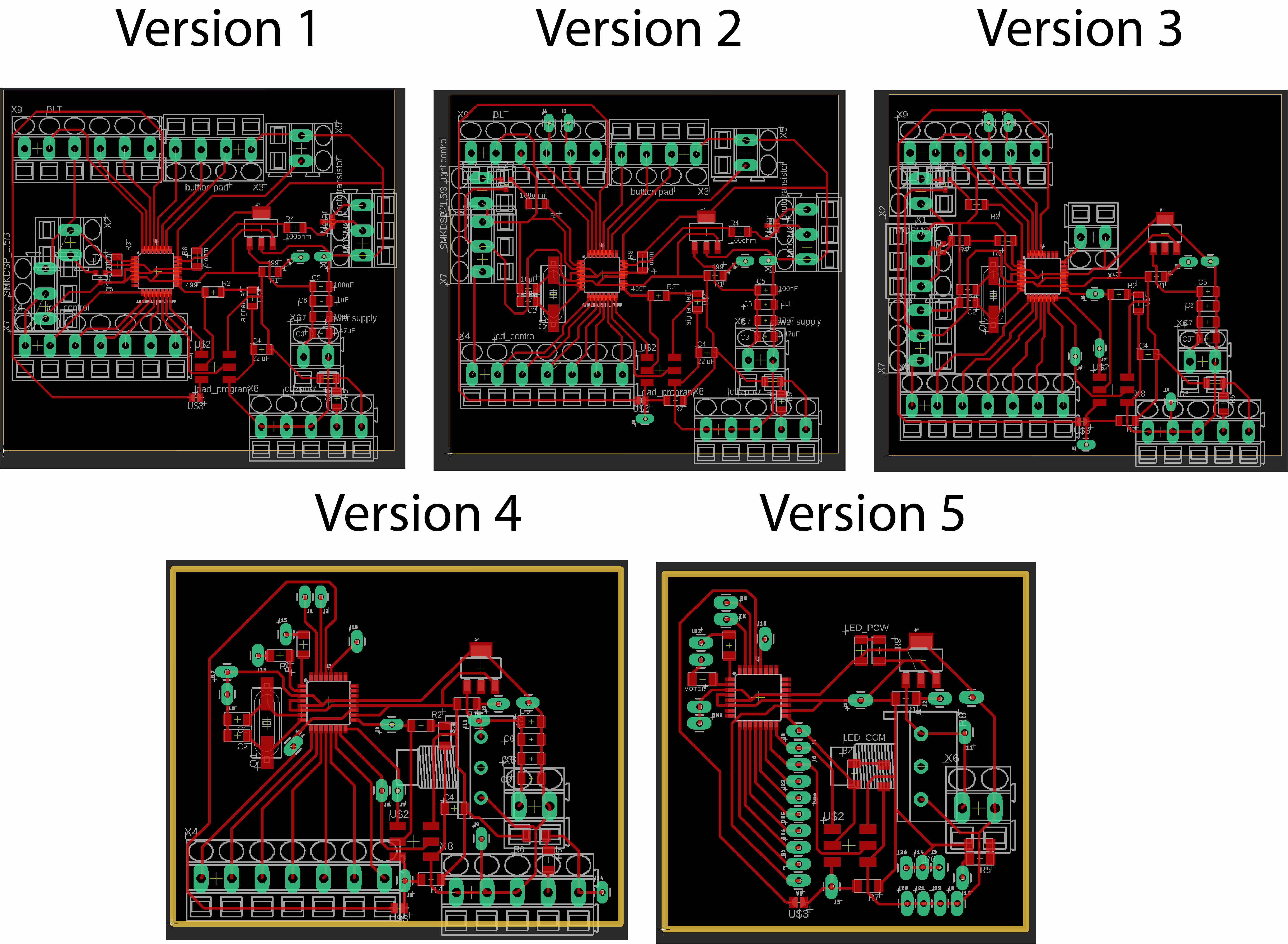
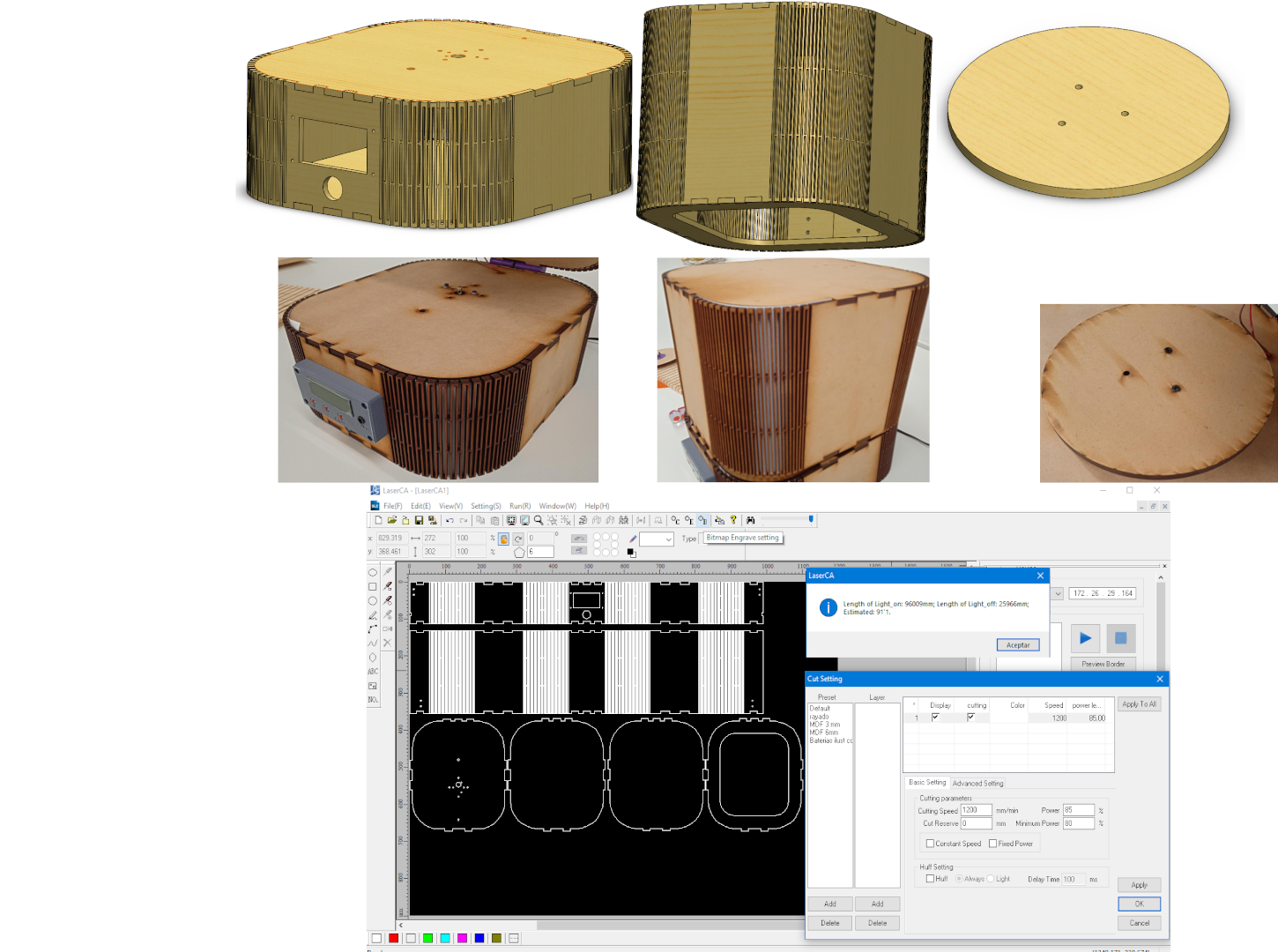
Chassis
here i'll drop a picture on the versions of the chassis.
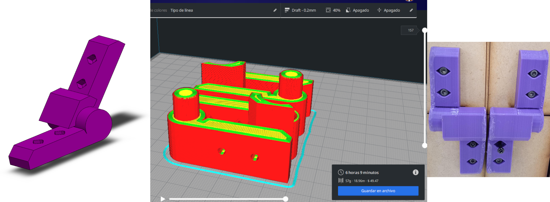
Hinges
here i'll drop a picture on the versions of the hinges.
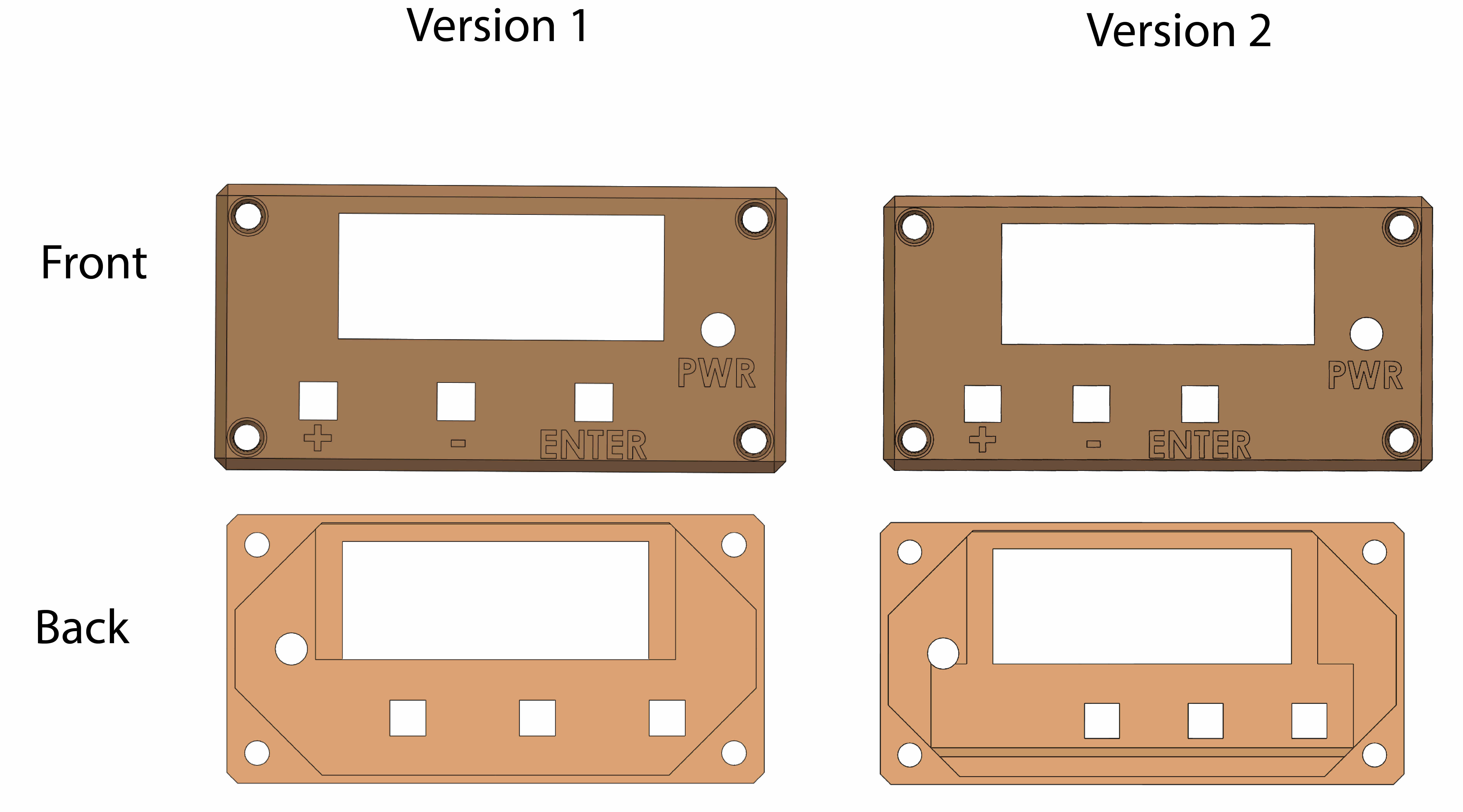
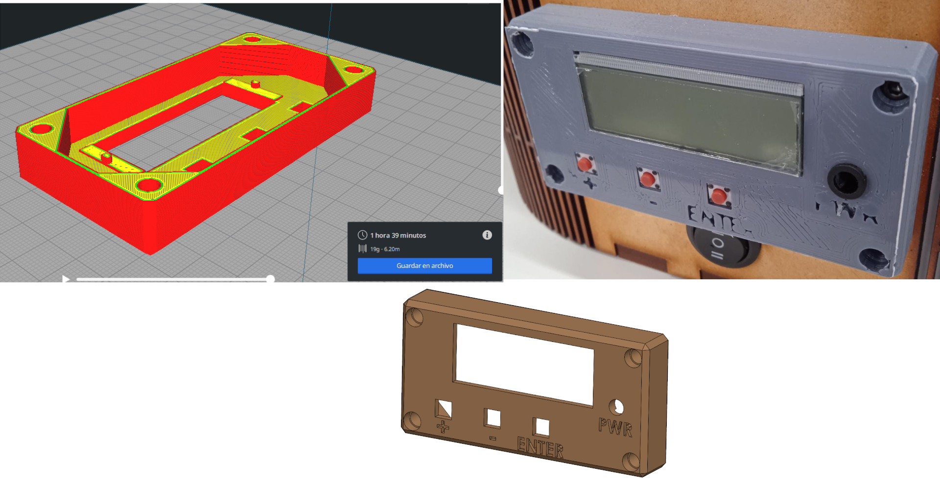
Housing
here i'll drop a picture on the versions of the housing for the display and Botton pad.
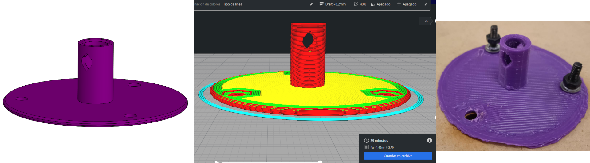
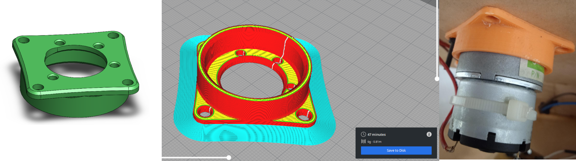
Shaft Coupler
here i'll drop a picture on the versions of the Shaft coupler.
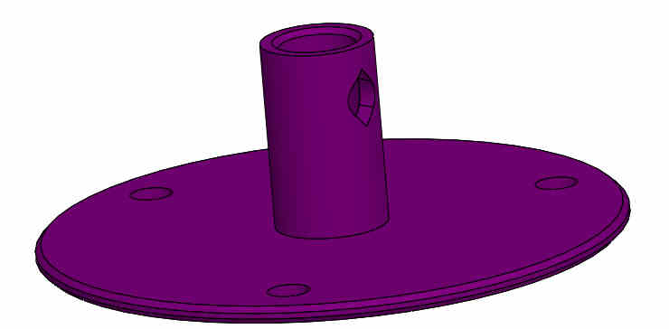
the only version on the shaft coupler but what can be better.
Motor Bracket
here i'll drop a picture on the versions of the motor bracket.
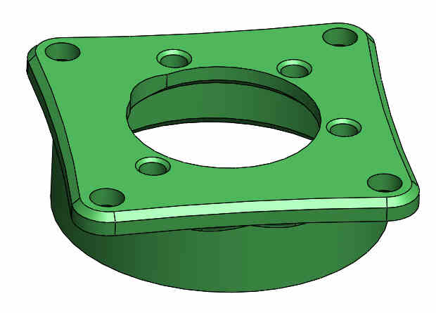
Picture of the only model and what can be better.
Wire router
here i'll drop a picture on the versions of the Wire router.
Picture of the only model and what can be better.
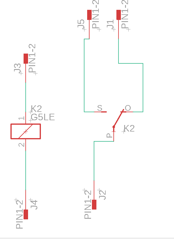
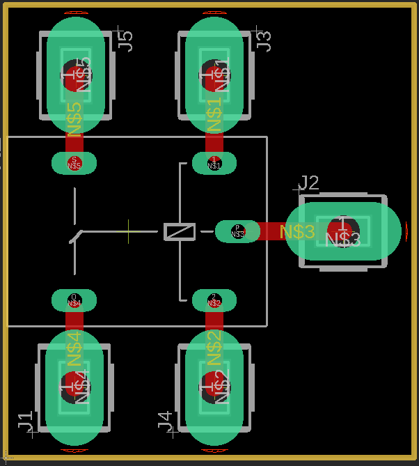
One Wire diagram
as an advice of my global instructor luis
i did a diagram on how the project works
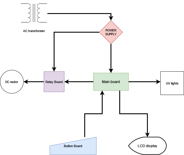
then the board turn on and off the relay board and the UV light modules
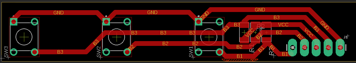
ECAD
here i'll drop a summary on all of the boards i've made.
i'm eager to try KIcad but i'm quite bussy with other softwares at the moment.
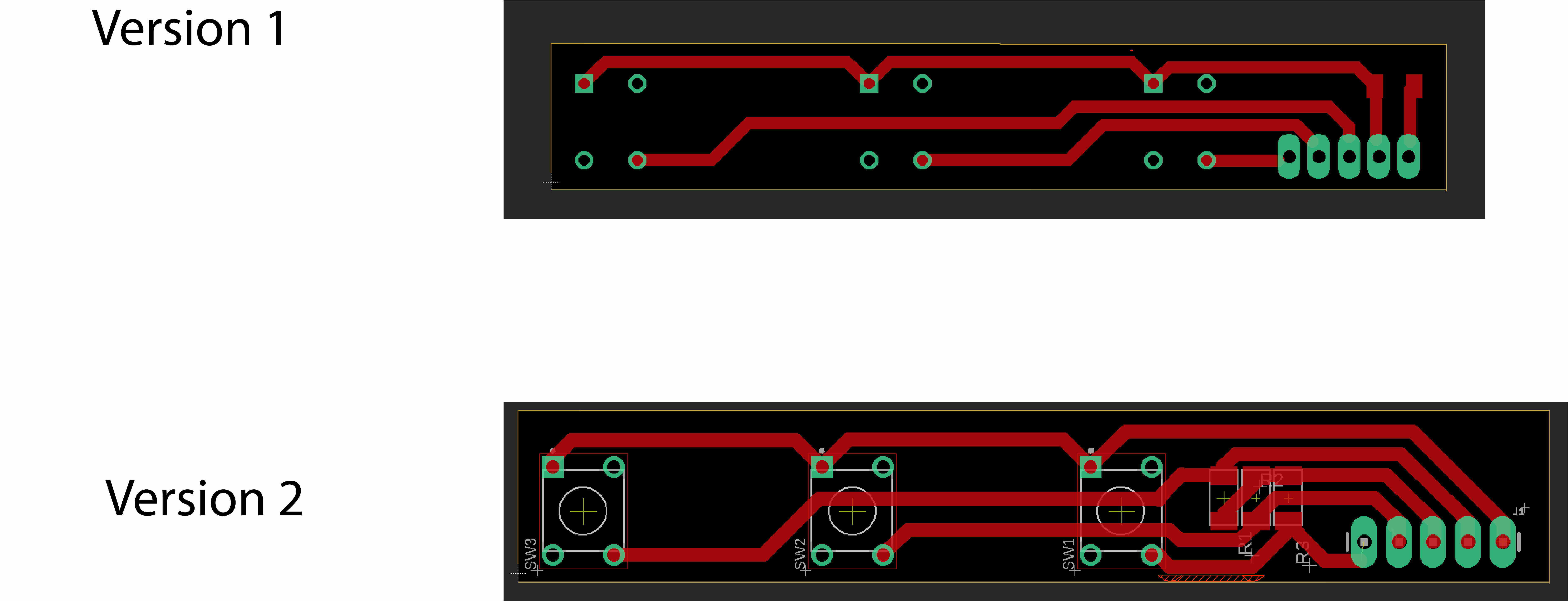
Relay board
here i'll drop a summary about the relay board.
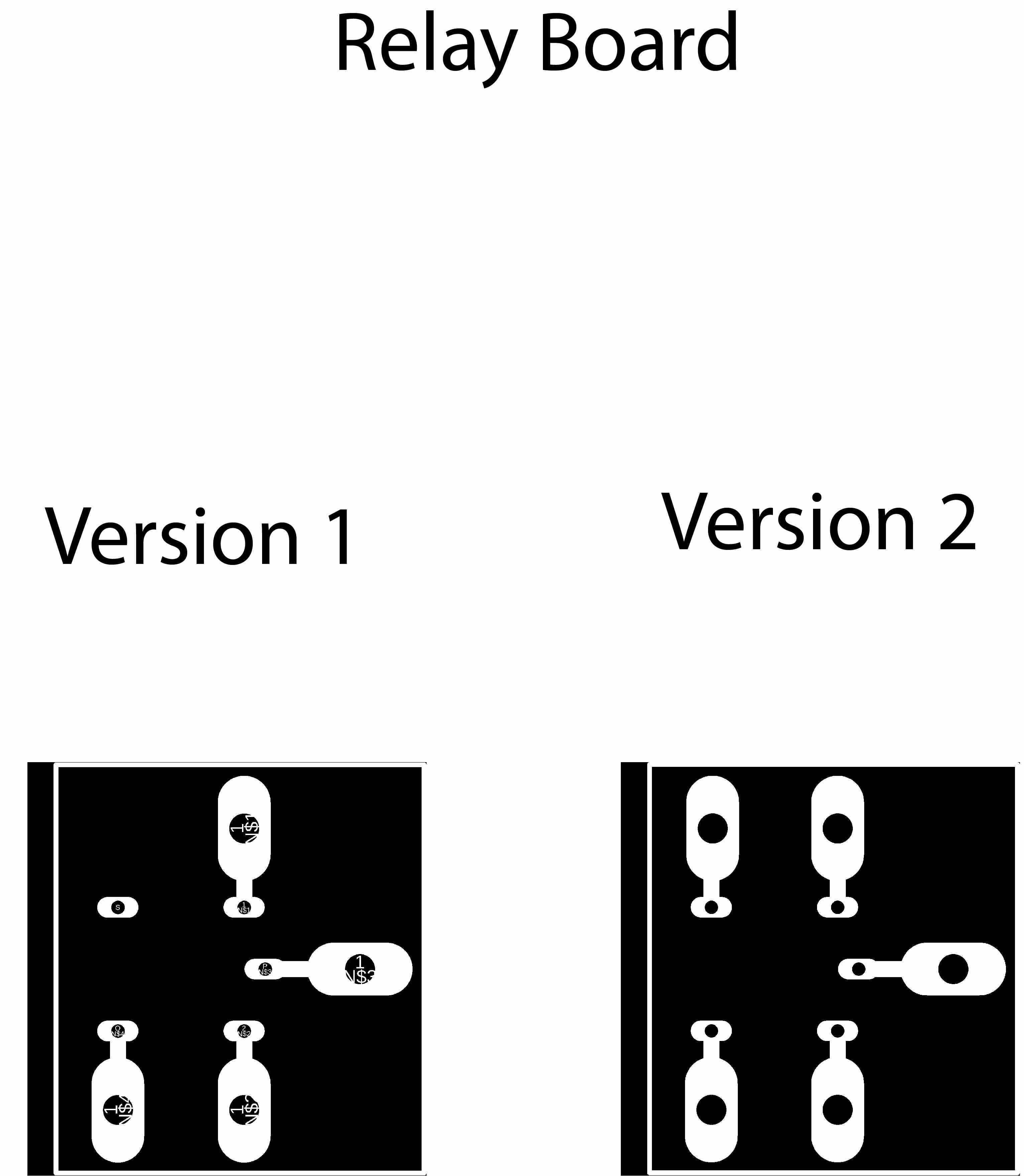
maybe a pic on all versions of the relay boards
Mainboard
here i'll drop a summary about the main board.
maybe a pic on all versions of the main board
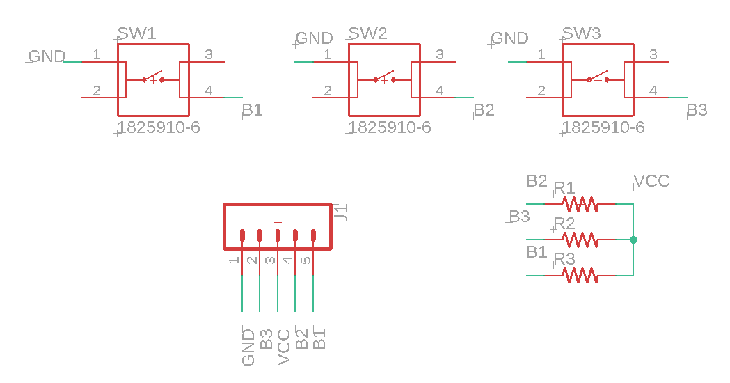
Button pad
here i'll drop a summary about the button pad.
maybe a pic on all versions of the Button pad
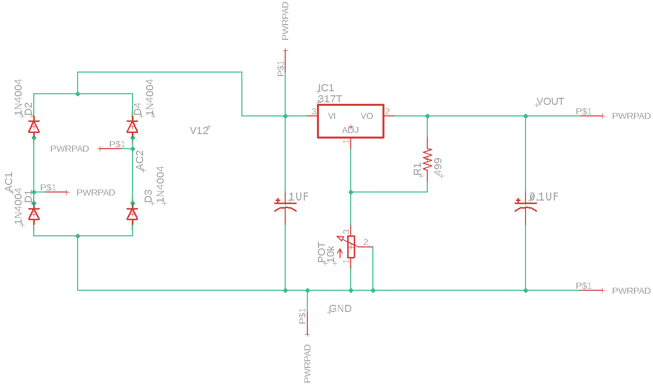
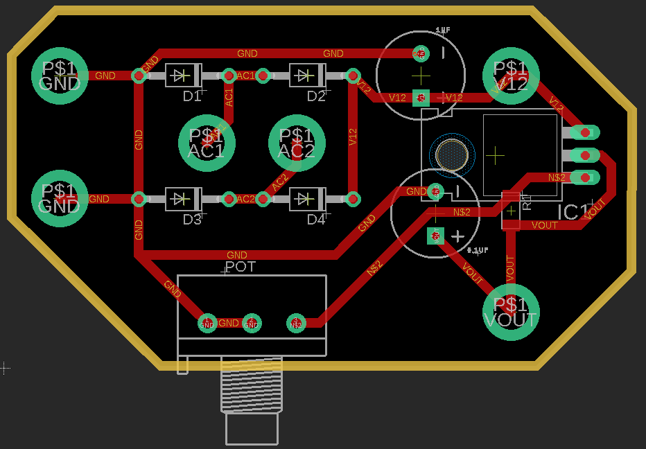
Power Supply
here i'll drop a summary about the power supply.
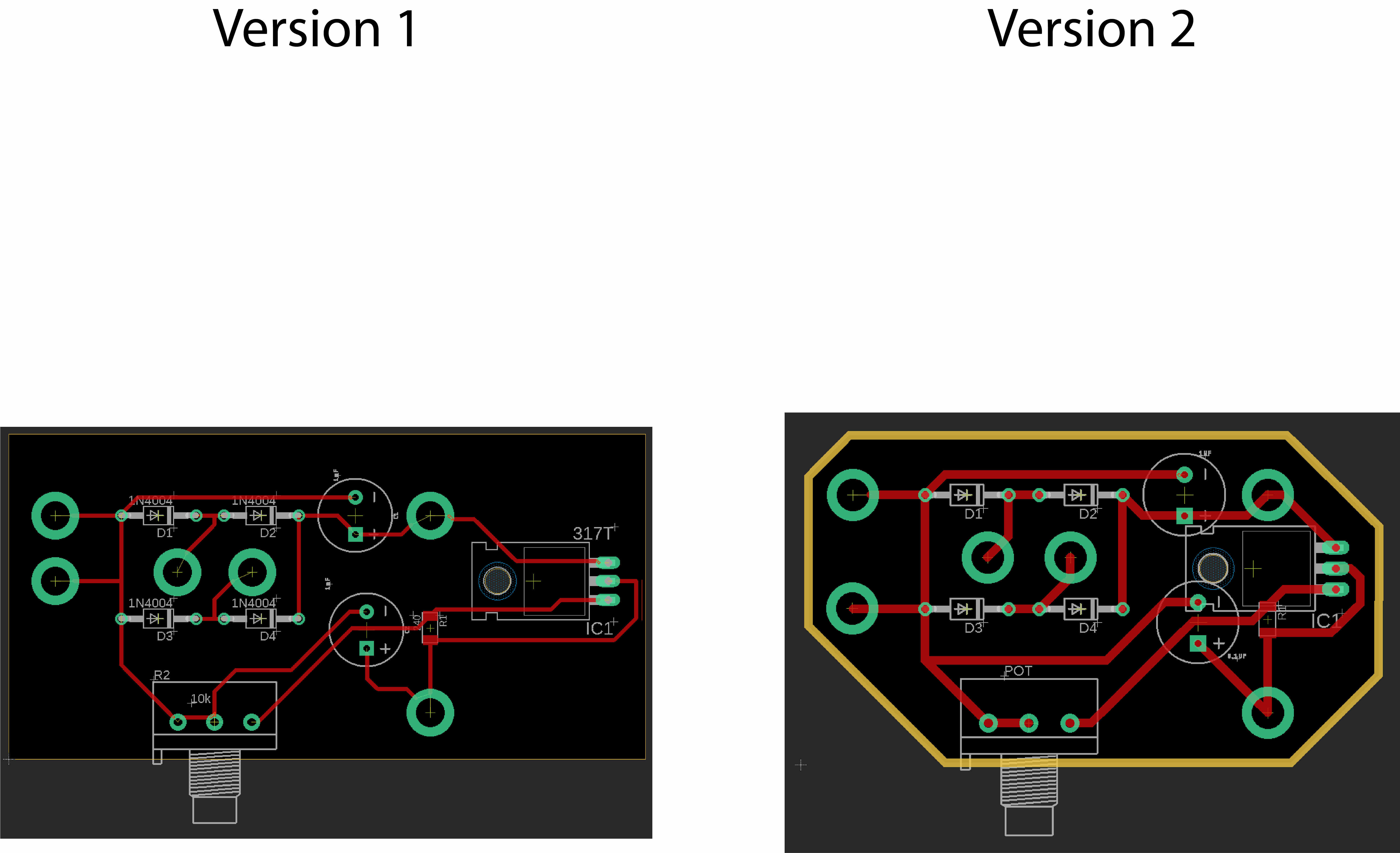
maybe a pic on all versions of the power supplies
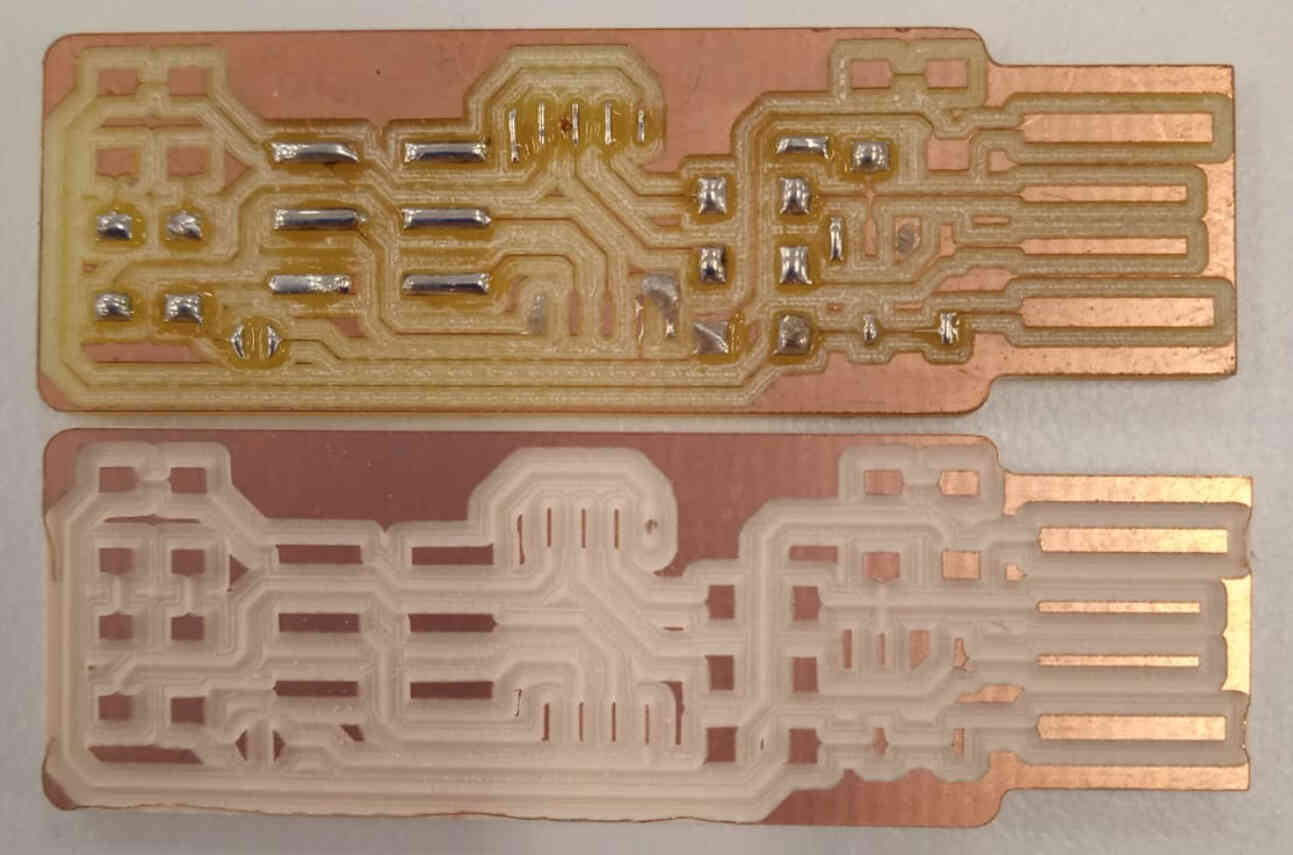
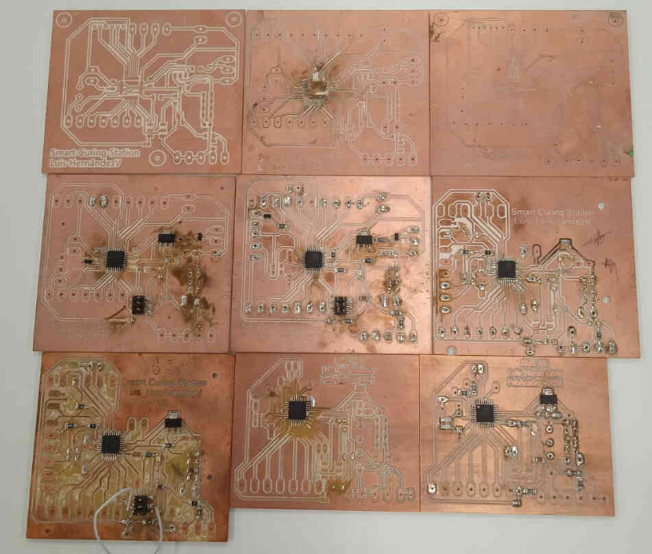
CAM and ECAM Bloppers
here i'll drop a summary on the mistakes i've made and what learn about them.
Electronics
here i'll drop a summary about what i did wrong on the roland machine and during soldering.
I will try to organize some stuff here.
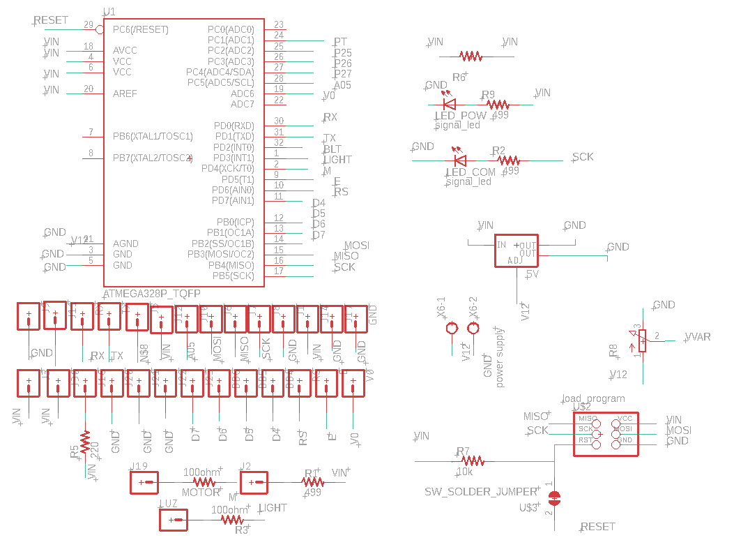
so i will begin this by saying that i have been working on the electrical design of thw board i'm that good with electronics yet but i think that this pcb design is good enough to begin to debug some electronic and programming issues
Resolution Related issues
i had to do a little bit of trial and error here to use 1200 dpi on eagle as a standard.
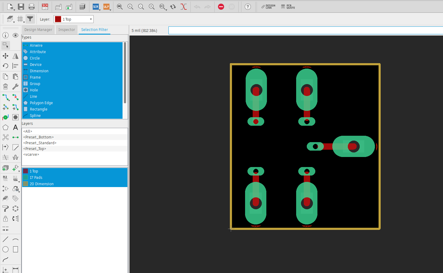
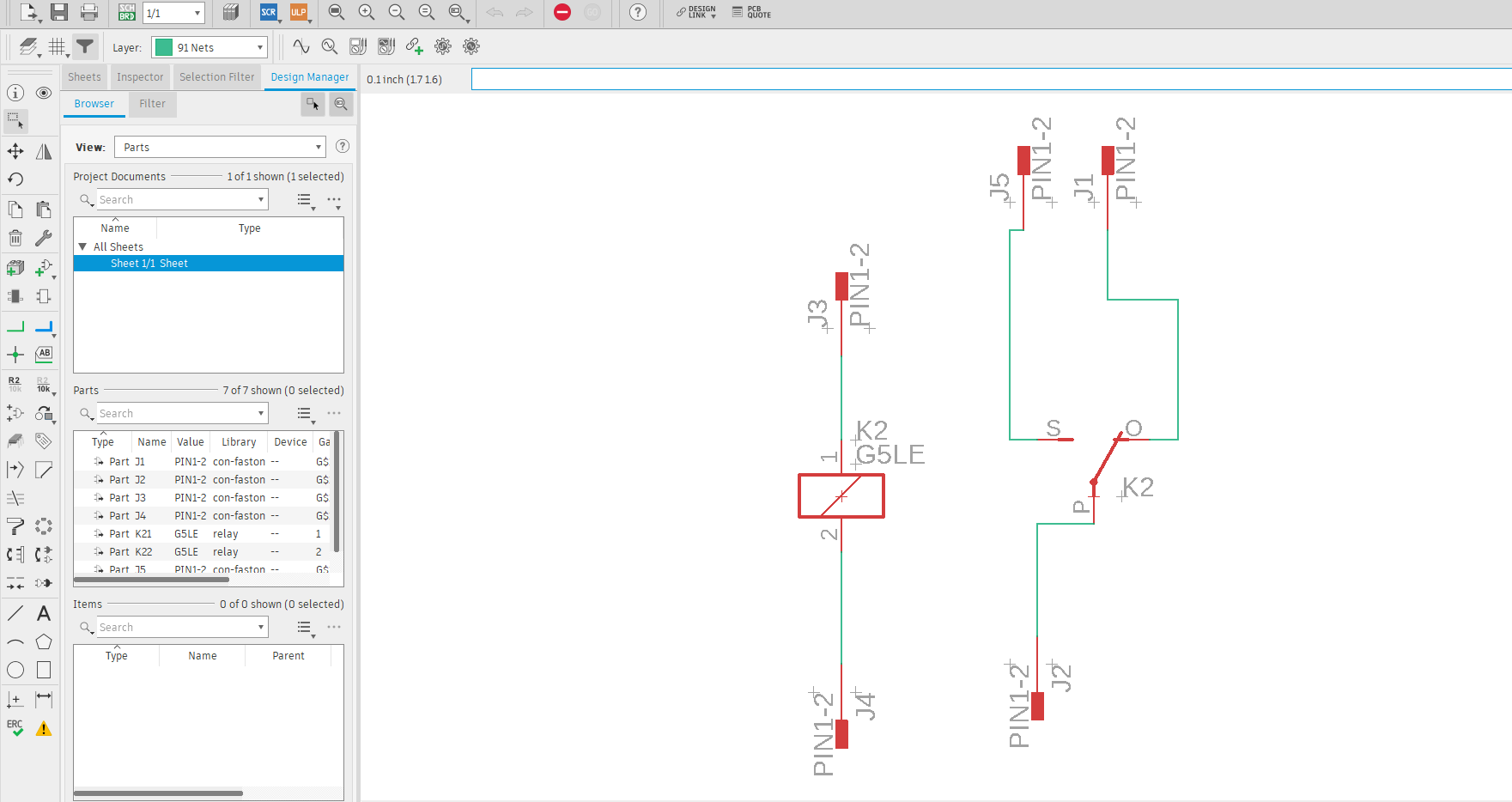
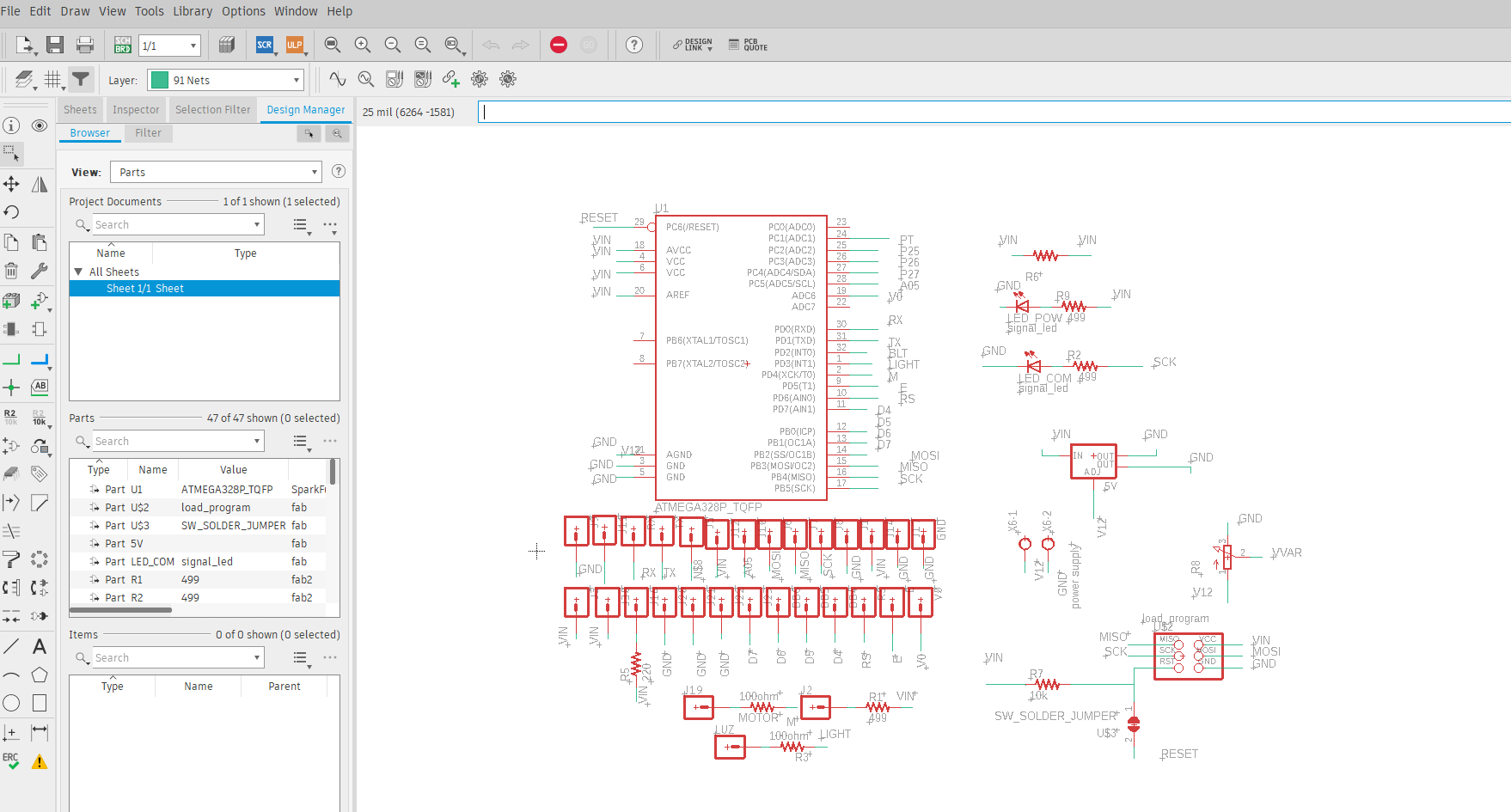
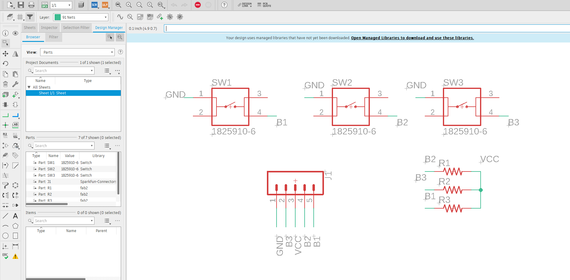
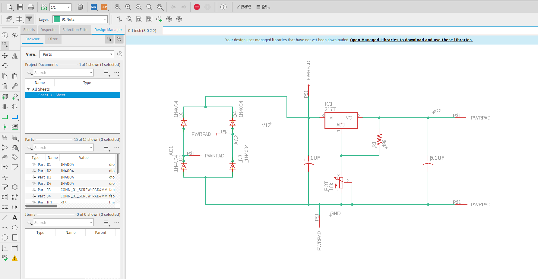
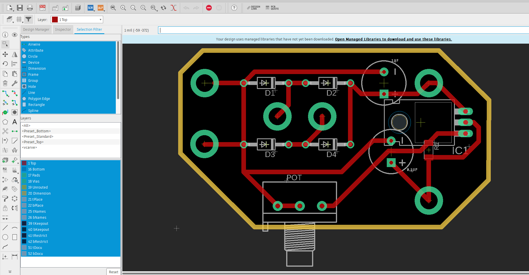
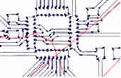
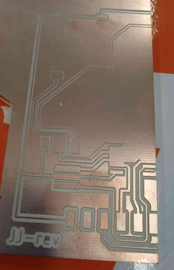
This is my eagle schematic for the control board
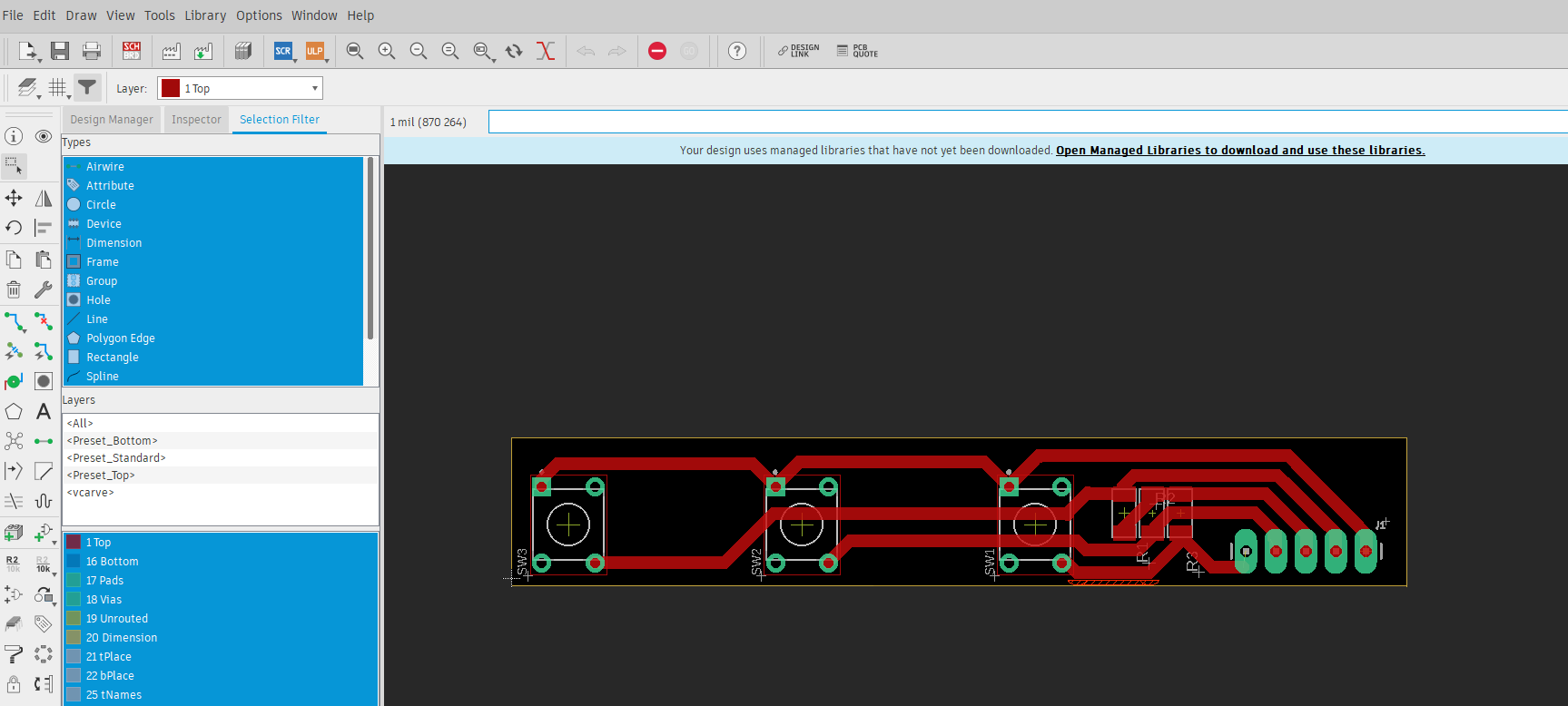
and This is my eagle board file for the control board as well.
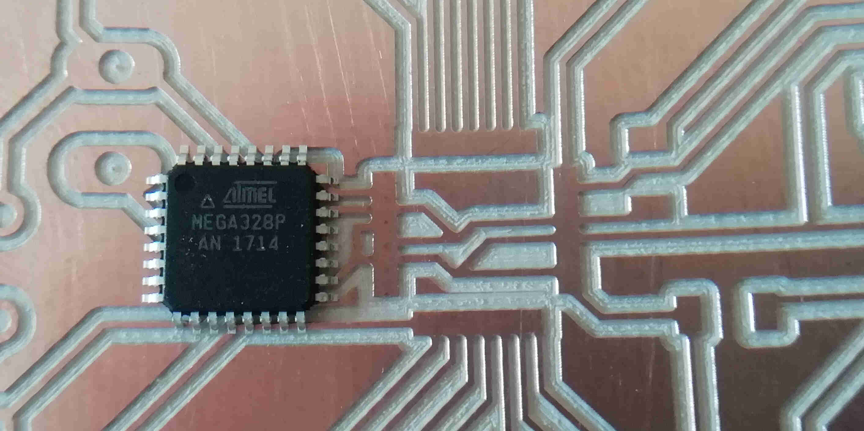
the first issue i had was that i choose to use the Atmega328p. But i could not find the block for the microprocessor within the eagle default libraries.
so i had to download the sparkfun_microcontroller library from the library manager in eagle.
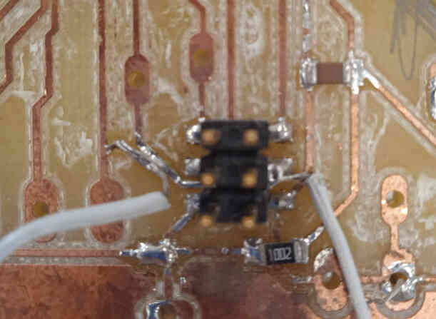
Next i wanted to use headers but since i only had wires with me and all of the routing will be inside the machine i supposed that will be ok to solder wires direcly into the boards. But that lead me to the next issue that was finding the right pads for soldering wires and have enough copper pad to solder to.
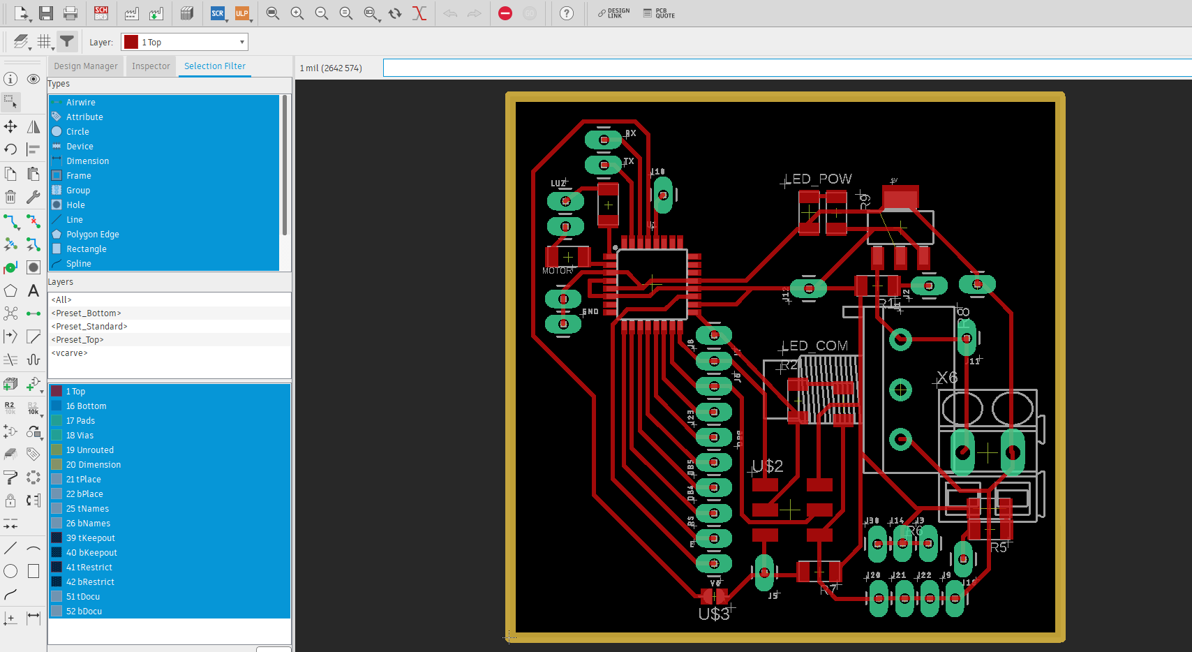
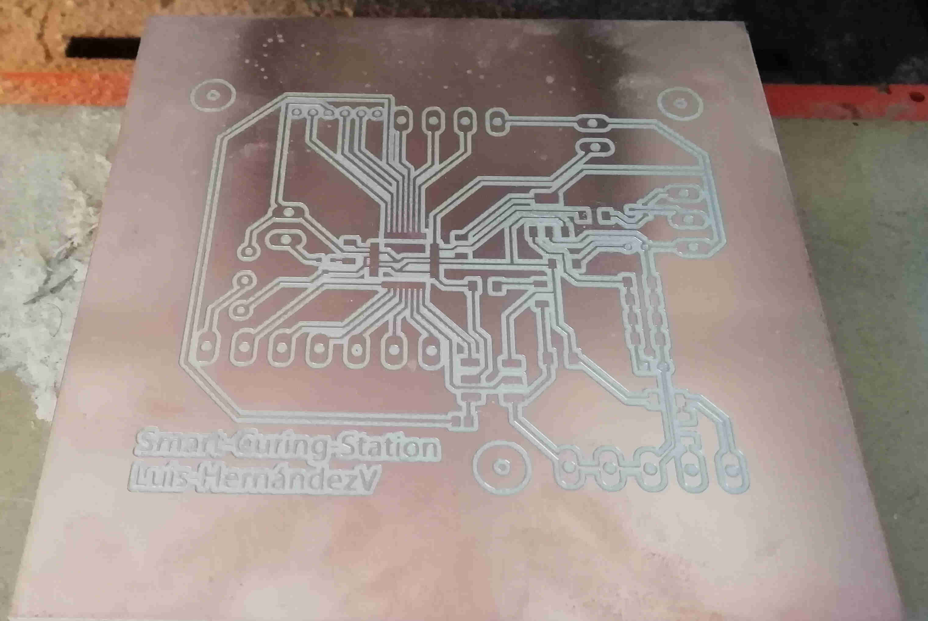
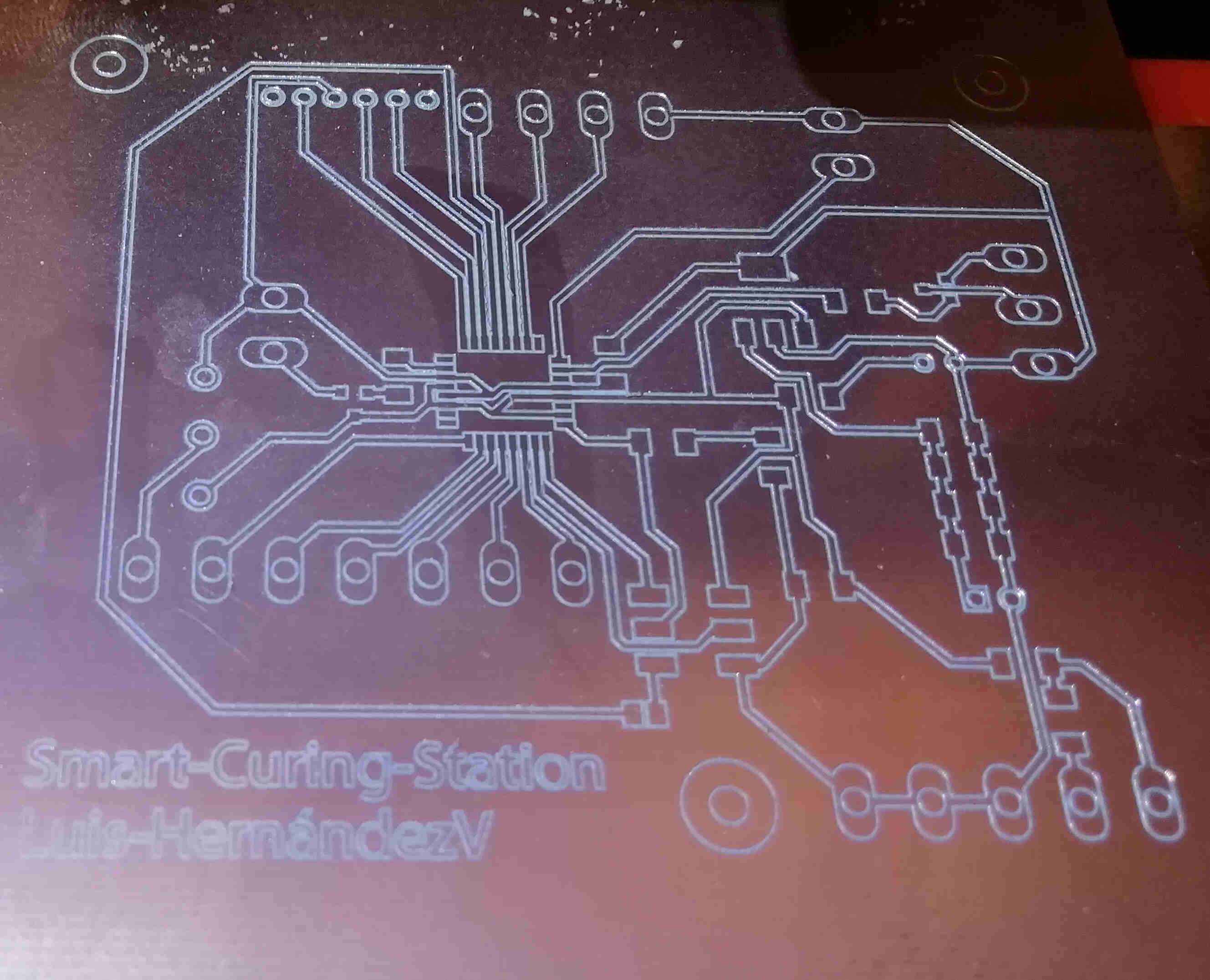
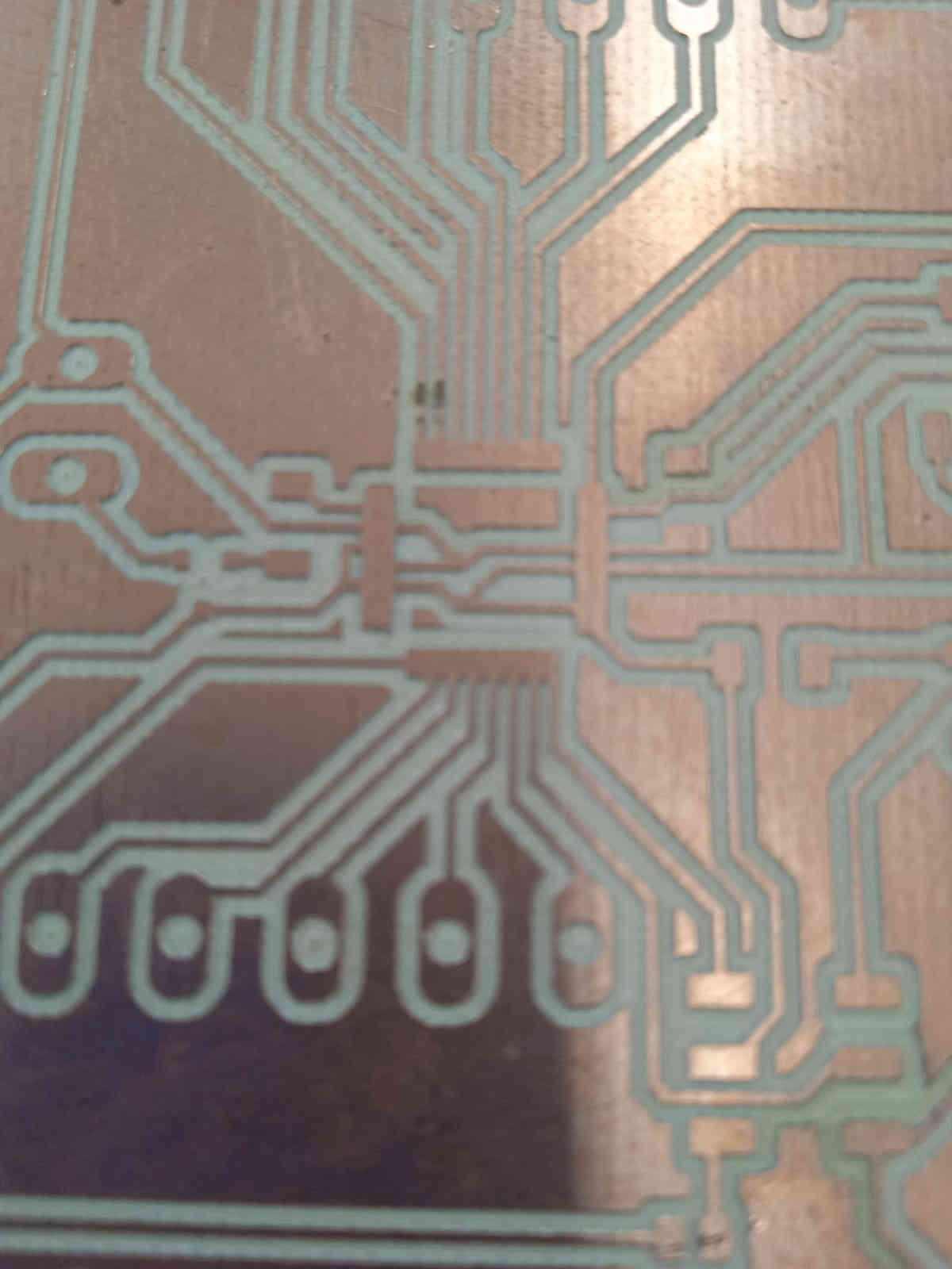
so i decided to use a plethora of pads i found. after doing all of the routing on eagle this was the final result.
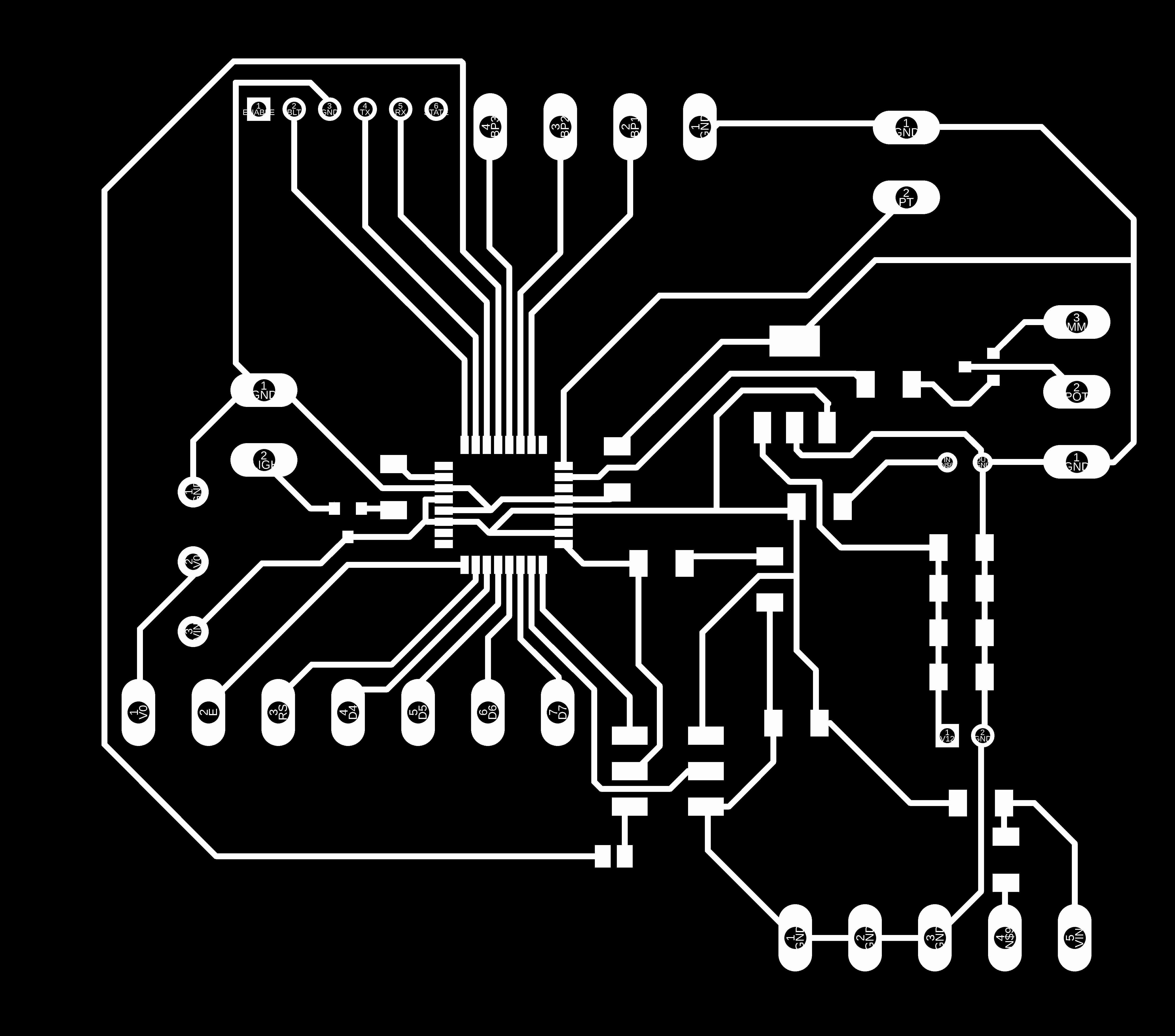
But here i noticed that i could not hide tha letters inside the holes of the pads for the wires. so i used illustrator to prepare the files and this was the result.
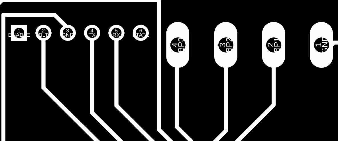
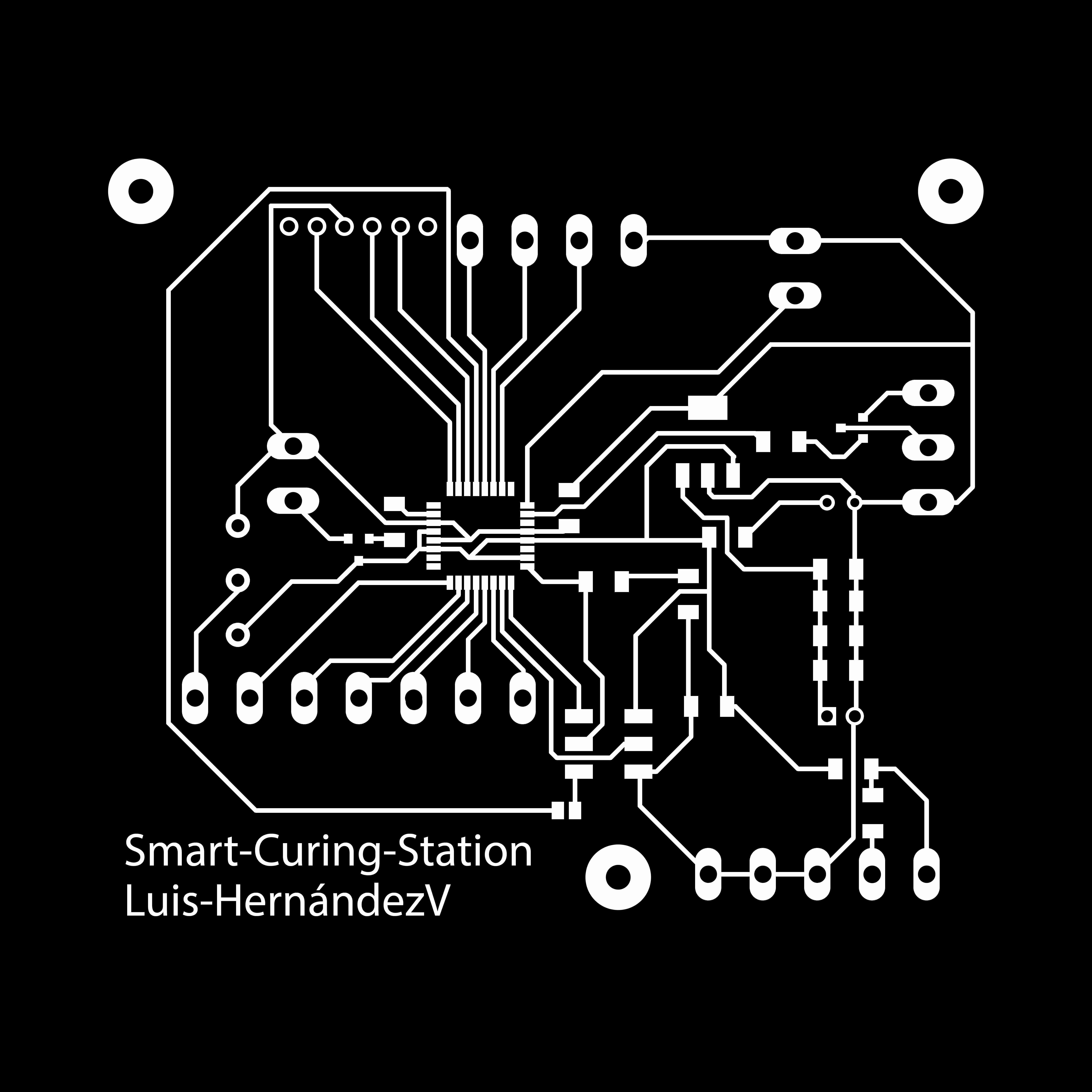
so i added the name of my final project and my name just to customize it a little.

then i went to fabmodules.org to create the toolpaths and here i used some settings i knew was working on the SRM-20 when i did the FabISP board back on electronics production week.
so i was sure this would work.
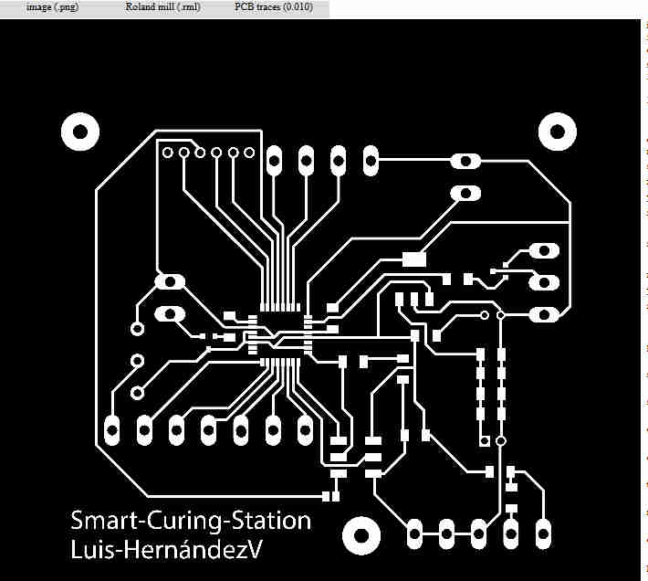
at first sight all seems ok so i went and saved the file. Then i used this carbide mill bit of 0.2 mm instead of the 0.01in that i used to create
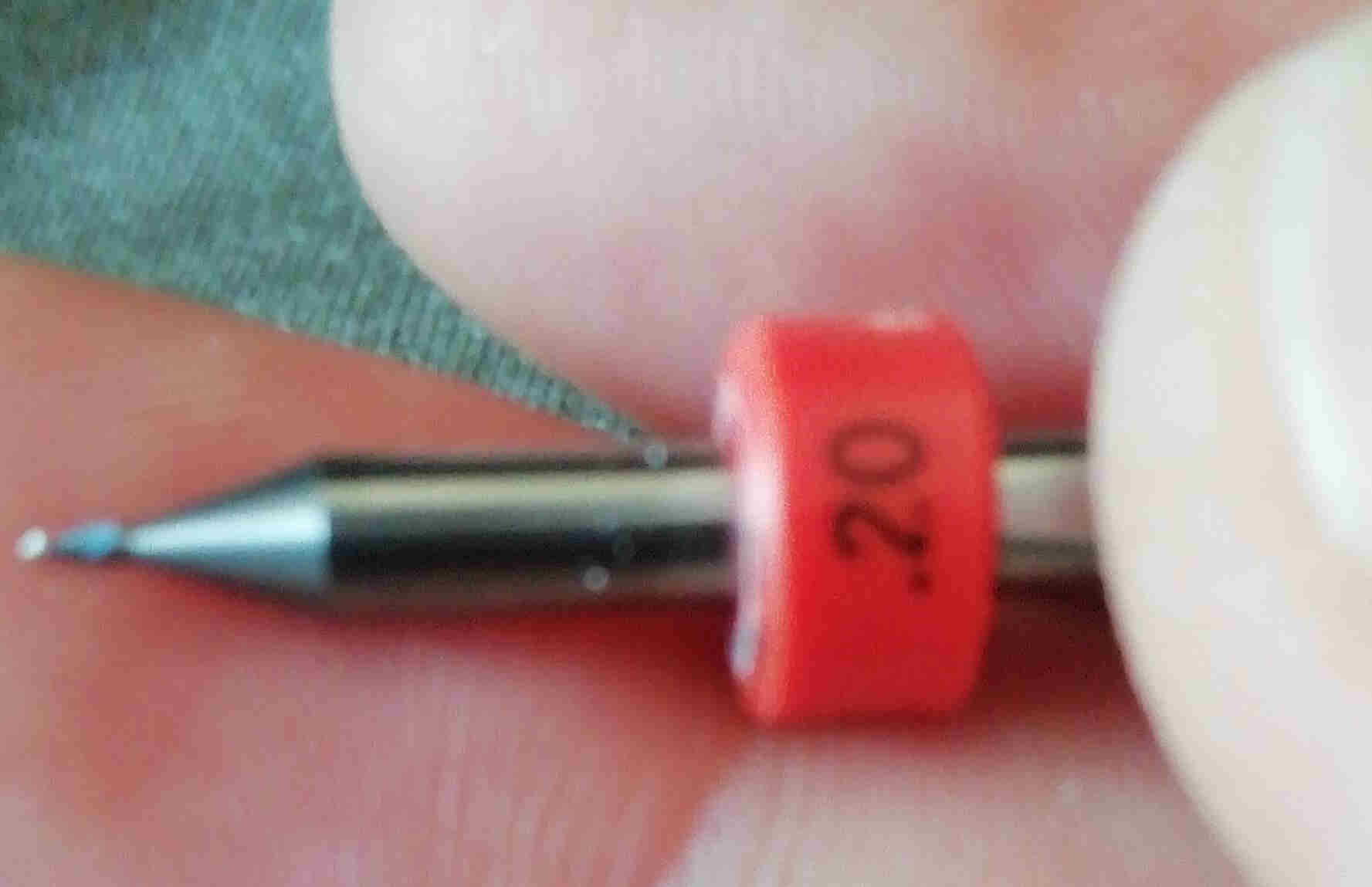
the diference is just 0.054mm so i figured that it would not be a problem so i loaded the file (.RML) on the SRM-20 and start milling it.
when finished i took it out from the machine to inspect the a little closer. Here is were i noticed that this milling bit is definitly supperior from the the first bit i used on electronics production week.
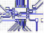
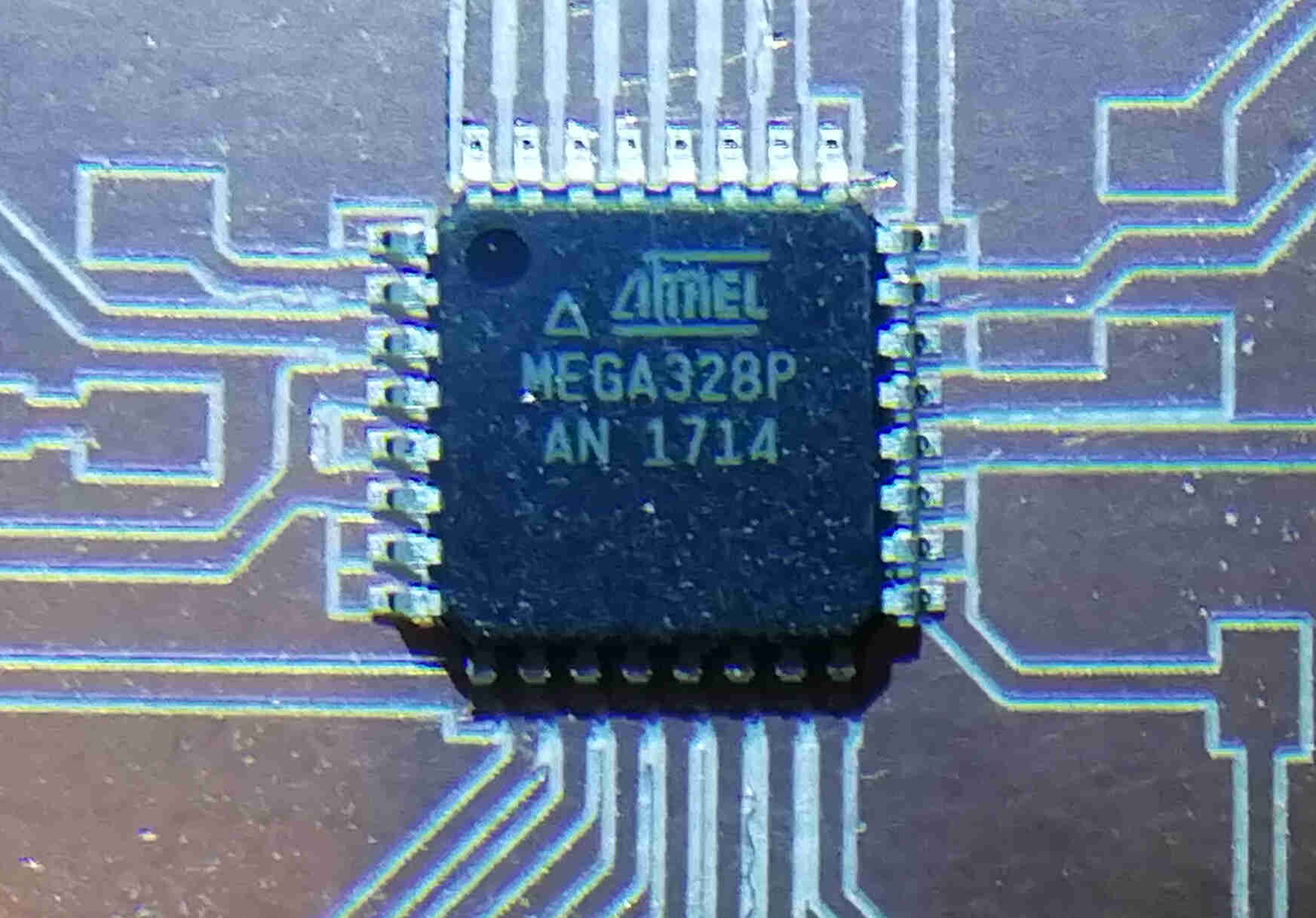
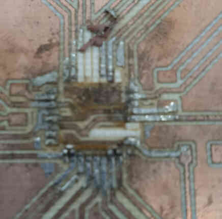
But it seemed that the spaces between the microprocessor pins were ignored.
zoom on the microprocessor pins
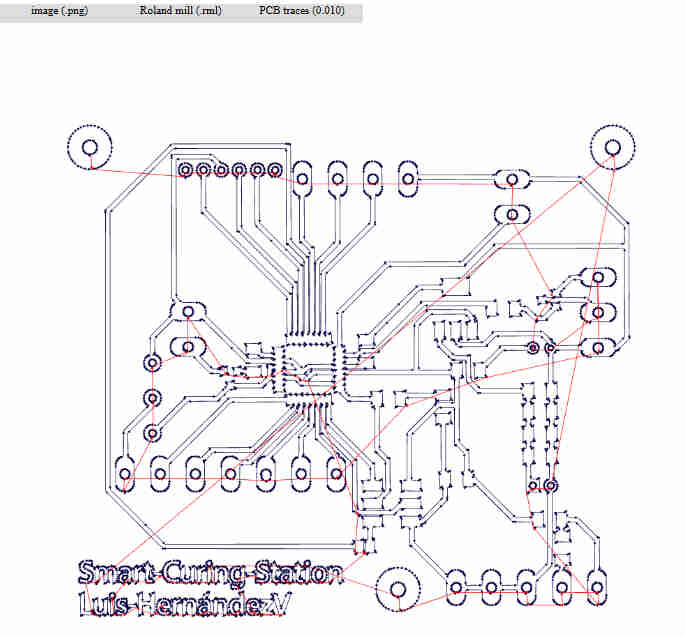
at first i tought the mill bit was wrong. But then i realized i did not double checked the toolpath in detail.
So i went and load again my settings on fabmodules and look at this.
i look that fabmodules is ignoring the space between the chip pins. i do not know why this is but i belive that has something to do with the size of my board.
Thanks to my instructor ivan hernandez for answering all of my questions today i could solve this.
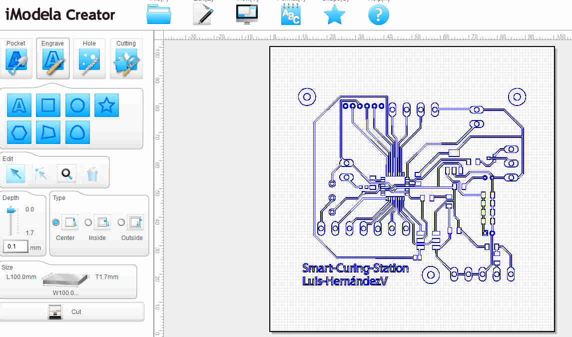
but i did not use fabmodules again .tough ...i used a software called imodela creator. Wich is a simple software created by roland to use some simple operations with the modela. Here you can draw simple shapes or import an image and extract it's contours.
so that's what i did and then i noticed that here i could compensate the diameter of the milling bit and when selecting cut you can not play with the settings enough or so i tought before i click on milling parameters. Here i could twitch the settings for the bit i was using.
zoom on the space between the pins of the microprossesor
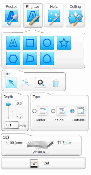
settings of the material and the cut depth
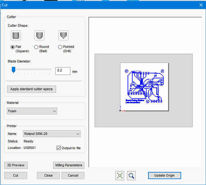
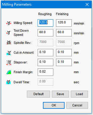 milling parameters
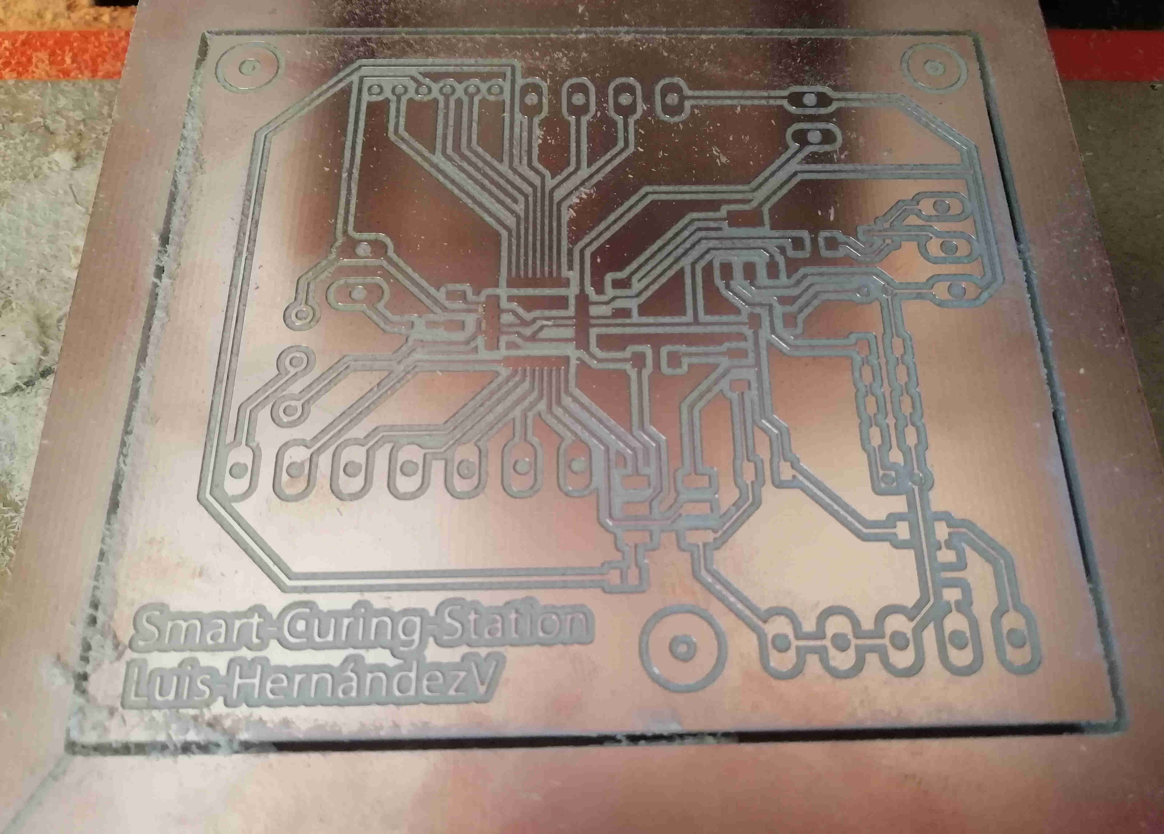
at the end i had to plunge the Z origin -0.06mm inside the material in order to get a clean cut. it seemed to be a little diference in precission between fabmodules and i modela creator but it maneged to get the job done.
and got rid of the copper that was on the first board.
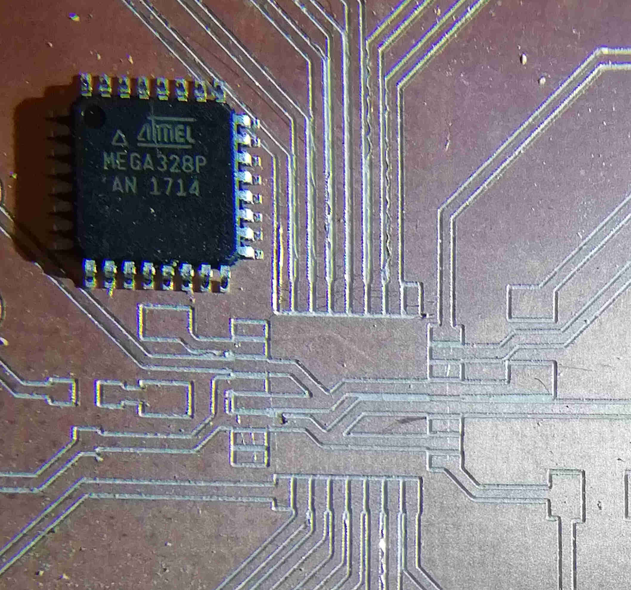
zoom on the pins where the atmega should be
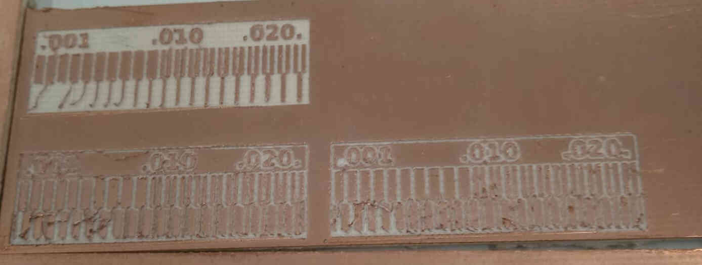
here is where i had yet another issue. it seemed that i choose good sized pads and wrong sized pads for soldering the wires.
i used a dremel tool in order to bore the holes into the board but had some troubles with doing so even with magnifying glass and all.
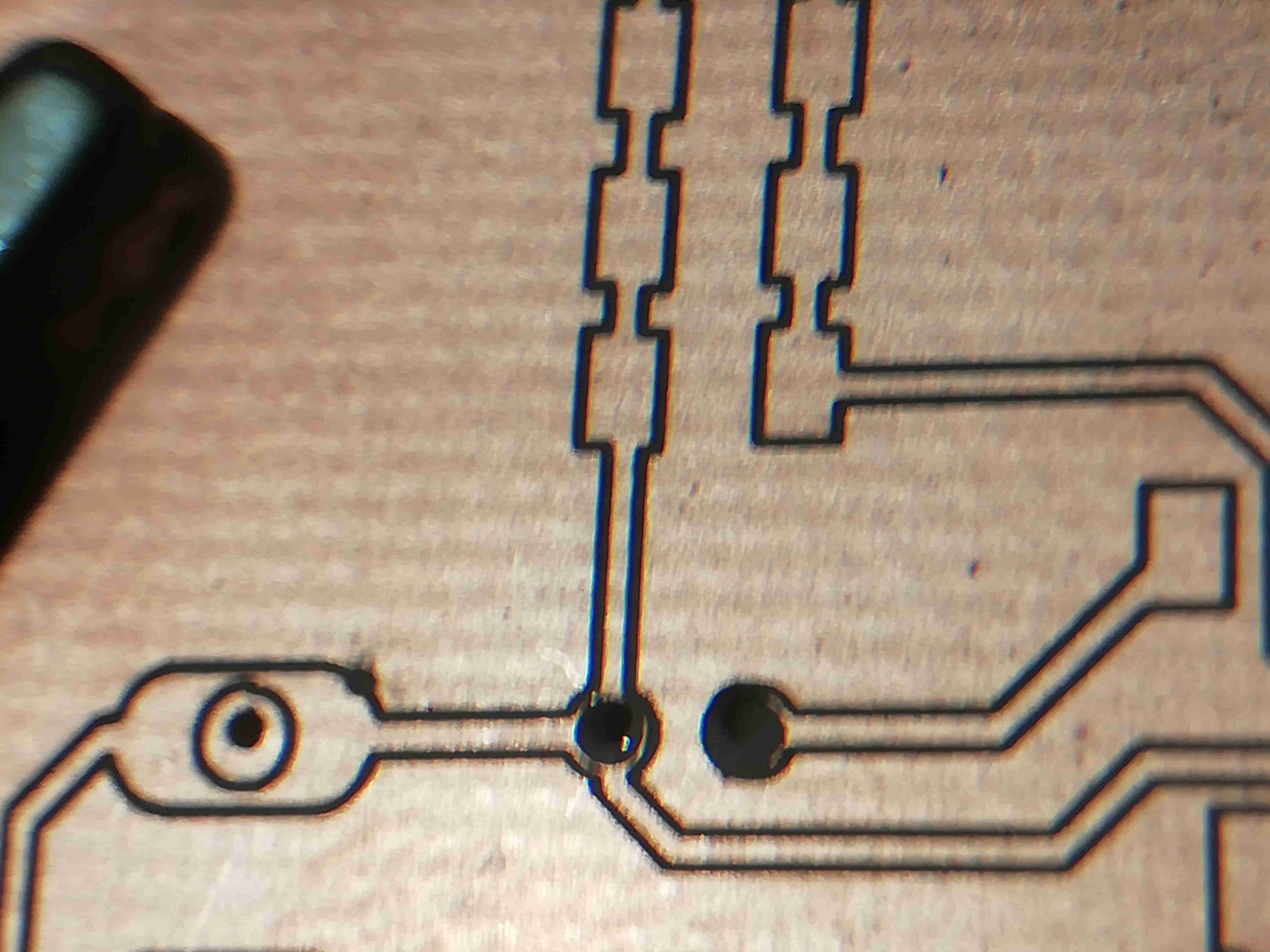
i had to test some tht pads in order to have a sweetspot between solder pad size and traces widths
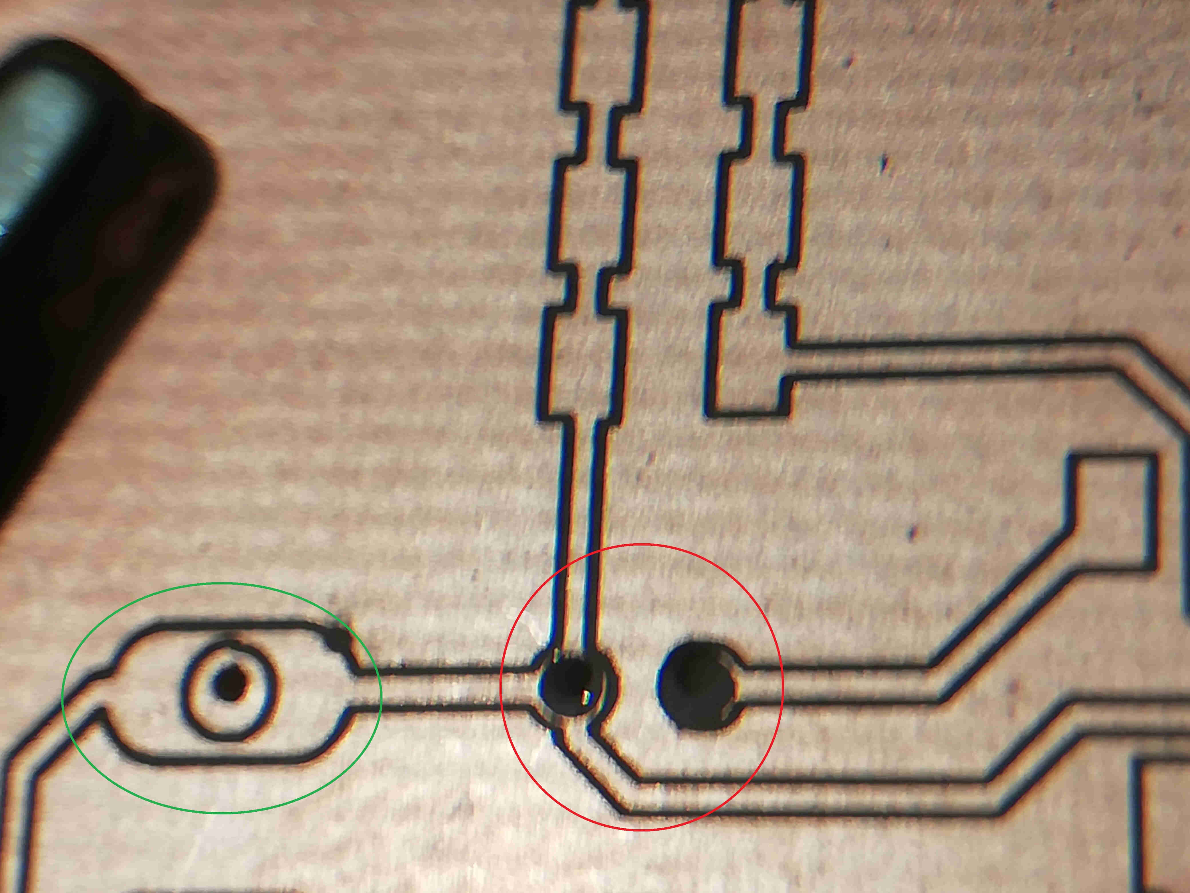
good pads size (green) bad pad sizing (red)
and here is where i left today
this previous issues ar about exporting on illustrator after creating the pads on eagle
this was before i leveled properly the bed obviusly

don't drill the holes by hand never
Time strategy
here i just going to post the image for the plan development
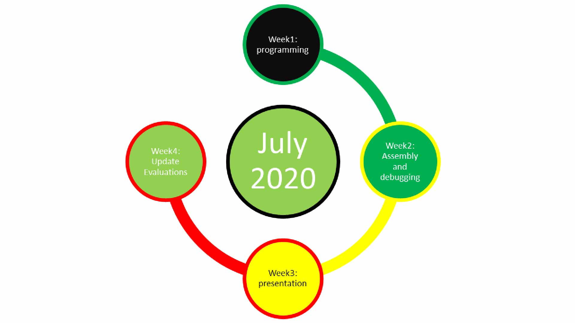
general plan for this last month before closure on the fabacademy 2020
Final project
BOM
Back to index
Final CAD/CAM
Back to index
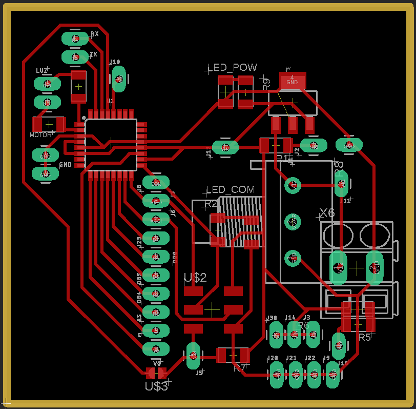
Final Sch and Brd files
Final Code
Final Testing on the code
Slide
Video
Links and references
Final Documents
CAD
native 2019 solidworks files.part1
native 2019 solidworks files.part2
native 2019 solidworks files.part3
Eagle board and schematic files
CAM
milling parameters for the roland files
here you can donwload that awsome pikachu model i used in the final presentation video by cyenyee page on thingiverse.
hereyou can check out the youtube channel of "el profe garcia" an awesome resource for electronics and programming in spanish language.
hereyou can check out the youtube channel of "Profe Pablo" an awesome resource for electronics and programming in spanish language.
hereyou can see how i managed to burn the bootloader without the external oscilator.
hereyou can check out my personal youtube chanel where i pretend to be uploading content about digital fabrication. basic topics of electronics and basic programming.