Workflow of assignment
Embedded Programming
An embedded system is a controller programmed and controlled by a real-time operating system with a dedicated function within a larger mechanical or electrical system, often with real-time computing constraints. It is embedded as part of a complete device often including hardware and mechanical parts.
Group Assignment:
1. Harvard architecture
The Harvard architecture is a computer architecture with physically separate storage and signal pathways for instructions and data. The term originated from the Harvard Mark I relay-based computer, which stored instructions on punched tape (24 bits wide) and data in electro-mechanical counters. These early machines had data storage entirely contained within the central processing unit, and provided no access to the instruction storage as data. Programs needed to be loaded by an operator; the processor could not initialize itself. Today, most processors implement such separate signal pathways for performance reasons, but actually implement a modified Harvard architecture, so they can support tasks like loading a program from disk storage as data and then executing it.
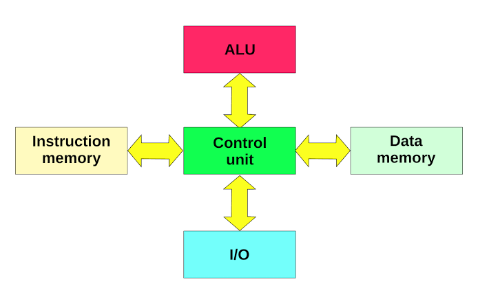
A. Memory:
In a Harvard architecture, there is no need to make the two memories share characteristics. In particular, the word width, timing, implementation technology, and memory address structure can differ. In some systems, instructions for pre-programmed tasks can be stored in read-only memory while data memory generally requires read-write memory. In some systems, there is much more instruction memory than data memory so instruction addresses are wider than data addresses.
B. Applications and features of Harvard Architectures:
The principal advantage of the pure Harvard architecture—simultaneous access to more than one memory system—has been reduced by modified Harvard processors using modern CPU cache systems. Relatively pure Harvard architecture machines are used mostly in applications where trade-offs, like the cost and power savings from omitting caches, outweigh the programming penalties from featuring distinct code and data address spaces. Digital signal processors (DSPs) generally execute small, highly optimized audio or video processing algorithms. They avoid caches because their behavior must be extremely reproducible. The difficulties of coping with multiple address spaces are of secondary concern to speed of execution. Consequently, some DSPs feature multiple data memories in distinct address spaces to facilitate SIMD and VLIW processing. Texas Instruments TMS320 C55x processors, for one example, feature multiple parallel data buses (two write, three read) and one instruction bus. Microcontrollers are characterized by having small amounts of program (flash memory) and data (SRAM) memory, and take advantage of the Harvard architecture to speed processing by concurrent instruction and data access. The separate storage means the program and data memories may feature different bit widths, for example using 16-bit wide instructions and 8-bit wide data. They also mean that instruction prefetch can be performed in parallel with other activities. Examples include the PIC by Microchip Technology, Inc. and the AVR by Atmel Corp (now part of Microchip Technology).
C. The speed aspect:
A lot has been discussed about the Harvard architecture, but without the speed any architecture can’t be accepted. But in case of the Havard architecture the manufacturers have designed the architecture in such a way that it will be able to process the data with a much higher speed. Yes, all care has been taken so that the architecture can process data with a high speed.By implementing the same formula the modern days CPU are being manufactured so that the new CPU can run with a much faster sped and can also process the data effectively. The concept of the CPU cache is also being implemented while designing the Harvard architecture.
2. Von Neumann Architecture:
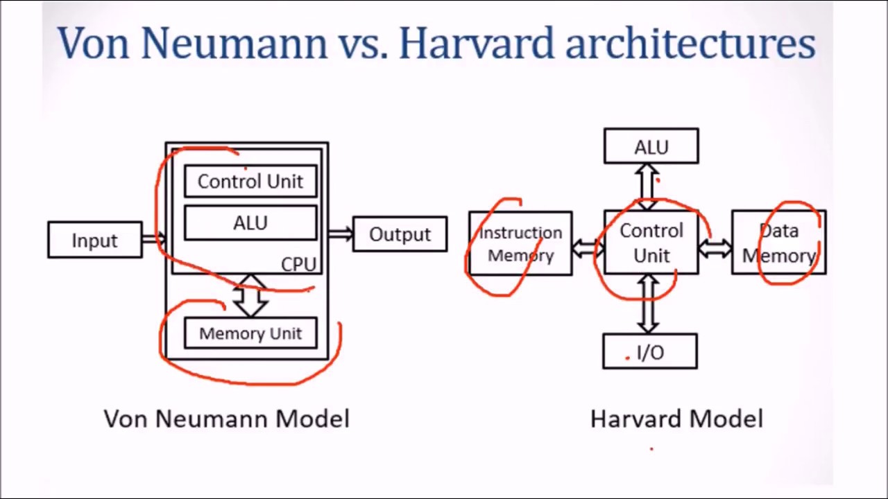
The von Neumann architecture, which is also known as the von Neumann model and Princeton architecture, is a computer architecture based on the 1945 description by the mathematician and physicist John von Neumann and others in the First Draft of a Report on the EDVAC. This describes a design architecture for an electronic digital computer with parts consisting of a processing unit containing an arithmetic logic unit and processor registers; a control unit containing an instruction register and program counter; a memory to store both data and instructions; external mass storage; and input and output mechanisms. The meaning has evolved to be any stored-program computer in which an instruction fetch and a data operation cannot occur at the same time because they share a common bus. This is referred to as the von Neumann bottleneck and often limits the performance of the system.
The design of a von Neumann architecture machine is simpler than that of a Harvard architecture machine, which is also a stored-program system but has one dedicated set of address and data buses for reading data from and writing data to memory, and another set of address and data buses for instruction fetching.
A.Applications and features of Von Neumann Architecture:
The Von Neuman architecture has got extensive application in everyday life. Keeping in mind the extensive application the Von Neuman architecture has been introduced as a subject in the engendering degree. From the third semester engineering students will have the subject as their curriculum. The Von Neuman architecture consists of some important features and here we will have a detailed elaboration to the features.
C. Control Unit:
This unit is mainly responsible for the controlling aspect. All the data stored in the memory and during the processing of data the control unit plays the role and it manages the data flow. In fact, to be more typically it is “One At A Time”. The control unit follows the principle of the One At A Time and accordingly it process all the data.
D. Input– output:
Like all electronics devices the Von Neuman architecture also has an input/output architecture. It is the basic function is same and nothing specially has been designed for the input and output architecture. With the Input and output device on a person can communicate with the device.
E. ALU:
ALU or the Arithmetic Logic Unit has a great importance in the Von Neuman architecture. Any sort of addition, subtraction, multiplication and division of the data will be carried out by this ALU. In addition to that any other kind of algorithmic function and activities will be carried out by the ALU. These are the basic aspect of the Von Neuman architecture which you must aware of.
Difference between Harvard and Von Neumann Architecture
A. Harvard Arhitecture:
a. The name is originated from “Harvard Mark I” a relay based old computer.
b. It required two memories for their instruction and data.
c. Design of Harvard architecture is complicated.
d. Harvard architecture is required separate bus for instruction and data.
e. Processor can complete an instruction in one cycle
f. Easier to pipeline, so high performance can be achieve.
g. Comparatively high cost.
B. Von Neumann Architecture:
a. It is named after the mathematician and early computer scientist John Von Neumann.
b. It required only one memory for their instruction and data.
c. Design of the von Neumann architecture is simple.
d. Von Neumann architecture is required only one bus for instruction and data.
e. Processor needs two clock cycles to complete an instruction.
f. Low performance as compared to Harvard architecture.
g. It is cheaper.
Raspberry Pi:
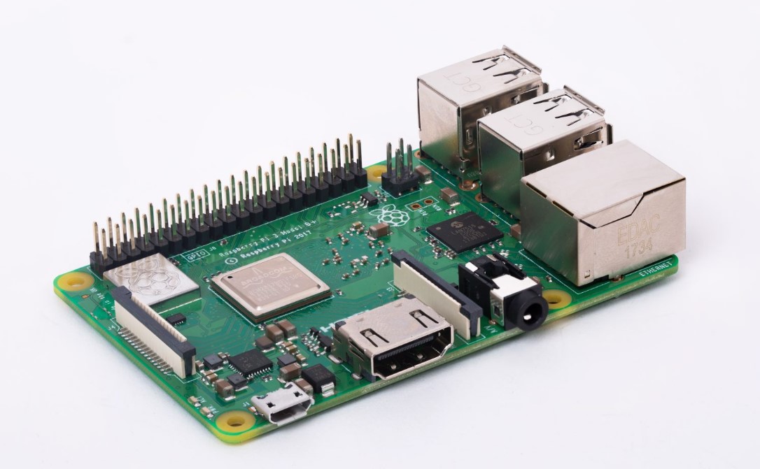
As part of the group assignment we all understood the basics of Raspberry Pi and programmed it.Raspberry Pi is a general-purpose computer, usually with a Linux operating system, and the ability to run multiple programs.
a. CHIP- Broadcom BCM2835 SoC
b. Core Architecture- ARM11
c. CPU- 700 MHz Low Power ARM1176JZFS
d. GPU- Dual Core VideoCore IV® Multimedia Co-Processor
e. Memory- 512MB SDRAM
f. Operating system- Boots from Micro SD card, running a version of the Linux operating system
g. Dimension- 85 x 56 x 17mm
h. Power- Micro USB socket 5V, 2A
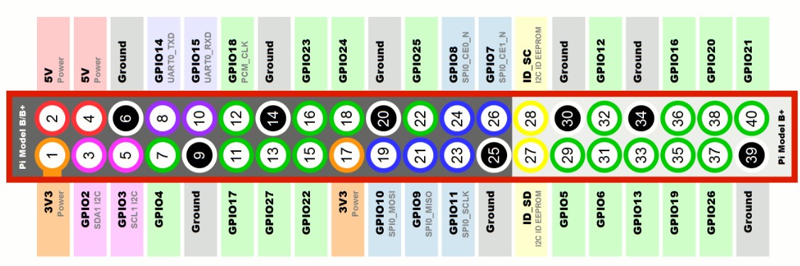
We referred the below pin out diagram for programming LED to blink:
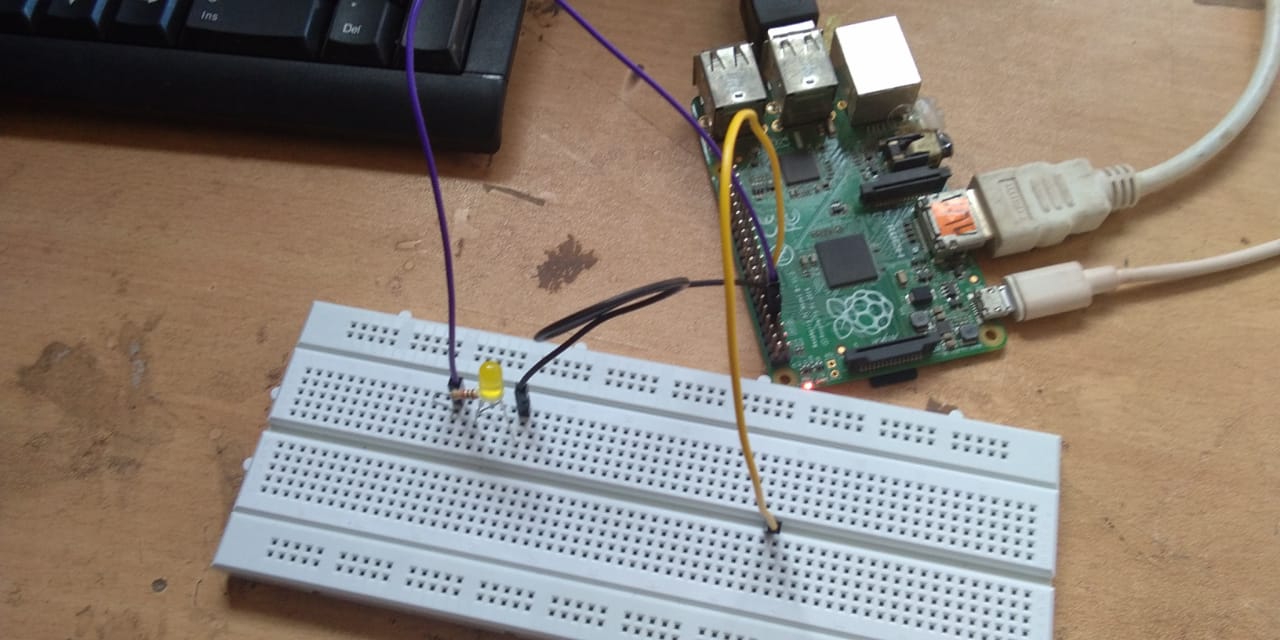
The picture below shows the setup and circuit connection:
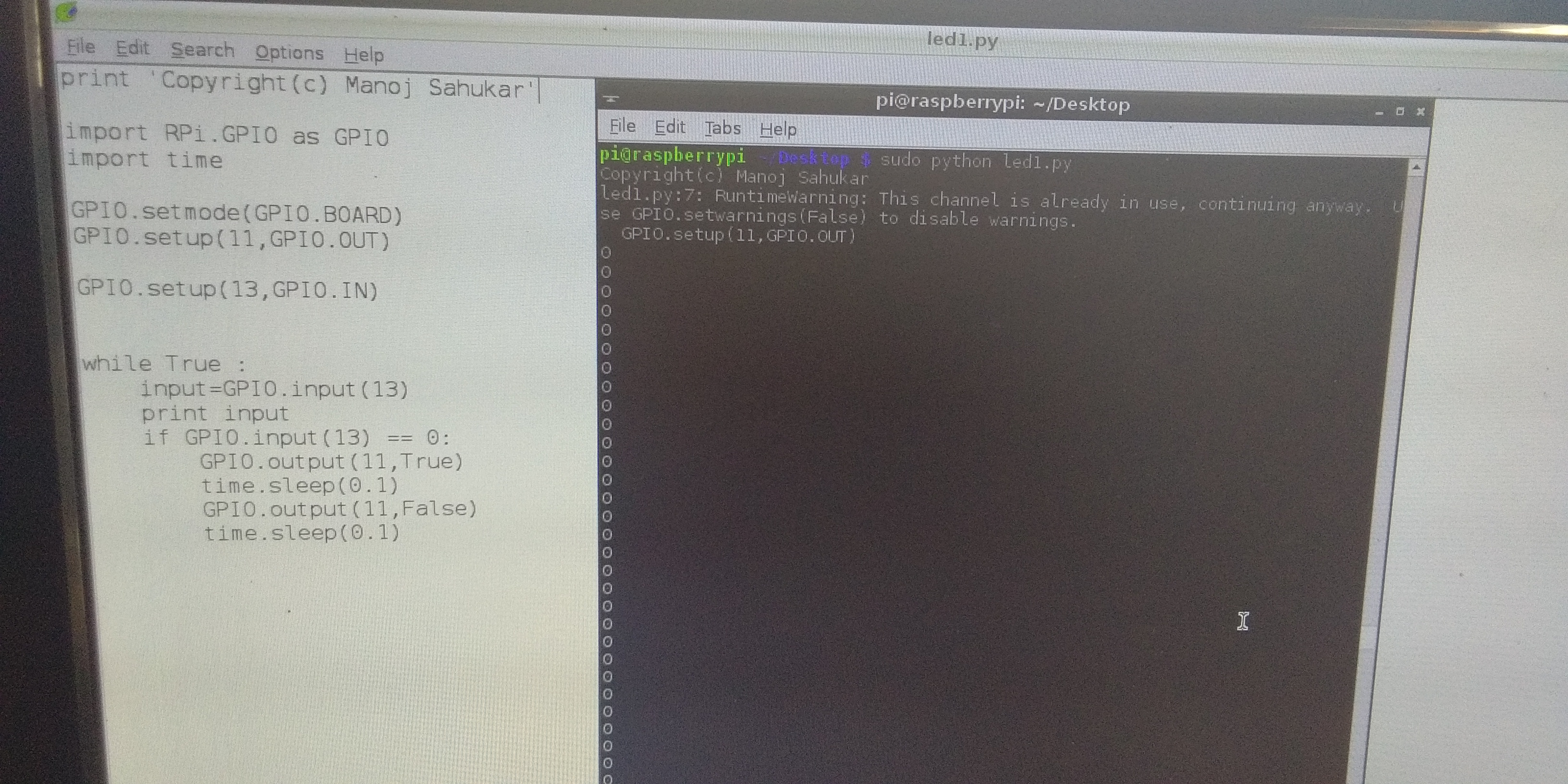
After loading the programme we got the LED blinking:
Comparison between "Arduino" and "Raspberry Pi" architectures:
a. Arduino has 0.002MB & Raspberry Pi has 512 MB memory.Clearly Raspberry Pi should be used for higher end applications.
b. Raspberry Pi is a fully functional computer while Arduino is a just microcontroller.
c. Arduino has 16 Mhz clock cycle and for Raspberry Pi it is 700Mhz.
d. Raspberry Pi has wired ethernet network on the other hand arduino doesnot have any network.
e. Arduino has 1 USB input whereas Rasperry Pi has 2.
f. Costwise there is no much difference.
Individual Assignment:
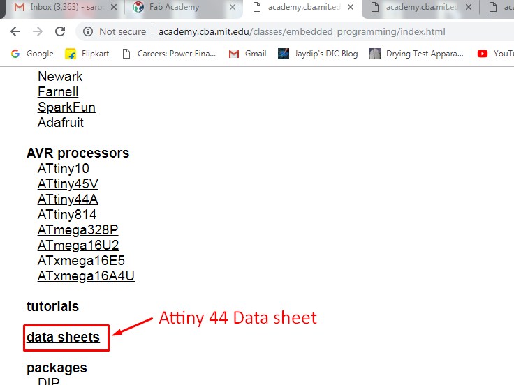
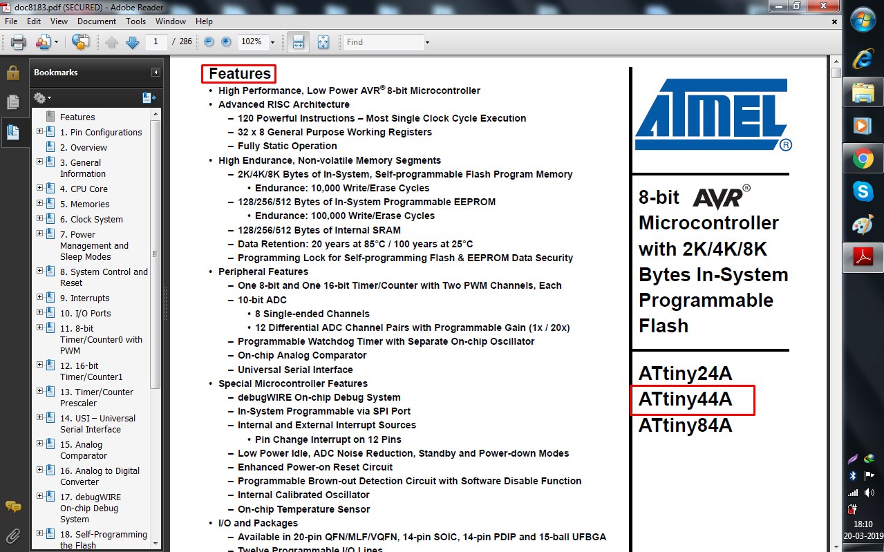
Firstly, I downloaded Attiny-44 uC datasheet from 'Fab academy 2019 > Schedule > Embedded programming week'.
You can download "Attiny 44 uC datasheet".
(Click Here)
Features of Attiny 44A:
Packages of Attiny 44A:
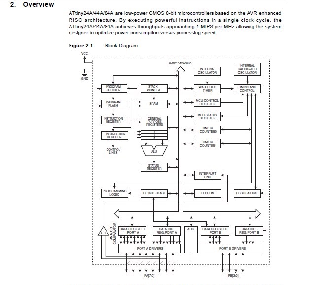
Architecture of Attiny 44A:
Memory and Clocks:
1. The CPU core runs on the AVR architecture.
2. The ATtiny24/44/84 chips have three different types of memory:
a. Data Memory (Static and Dynamic RAM). SRAM memory is used for storing your data which is processed during the run time (including also the registers) - volatile memory
b. The Program Memory is a reprogrammable flash memory that stores the program - non volatile. It can endure up to 10,000 write/erase cycles.
c. EEPROM memory can be used for storing non volatile data and changeable during run-time.
(for example: setting values) Endurance: 100,000 Write/Erase Cycles.
3. The chip contains four different clocks CPU Clock, I/O Clock, Flash Clock, and ADC Clock. The internal oscillator is the default clock and it runs at 8mHz.
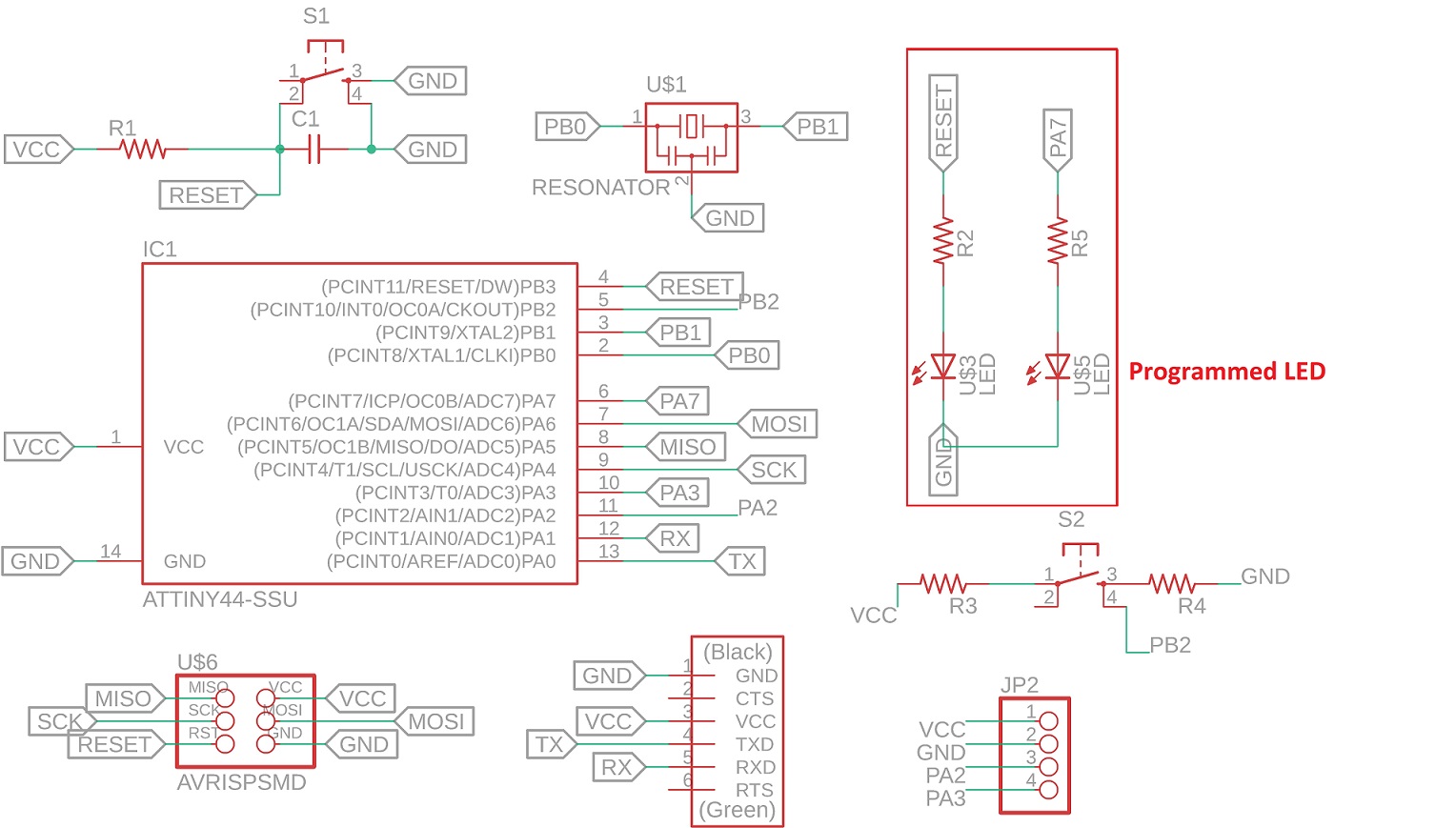
Programmed my “HelloWorld Board” using USBtinyISP in 'Arduino IDE':
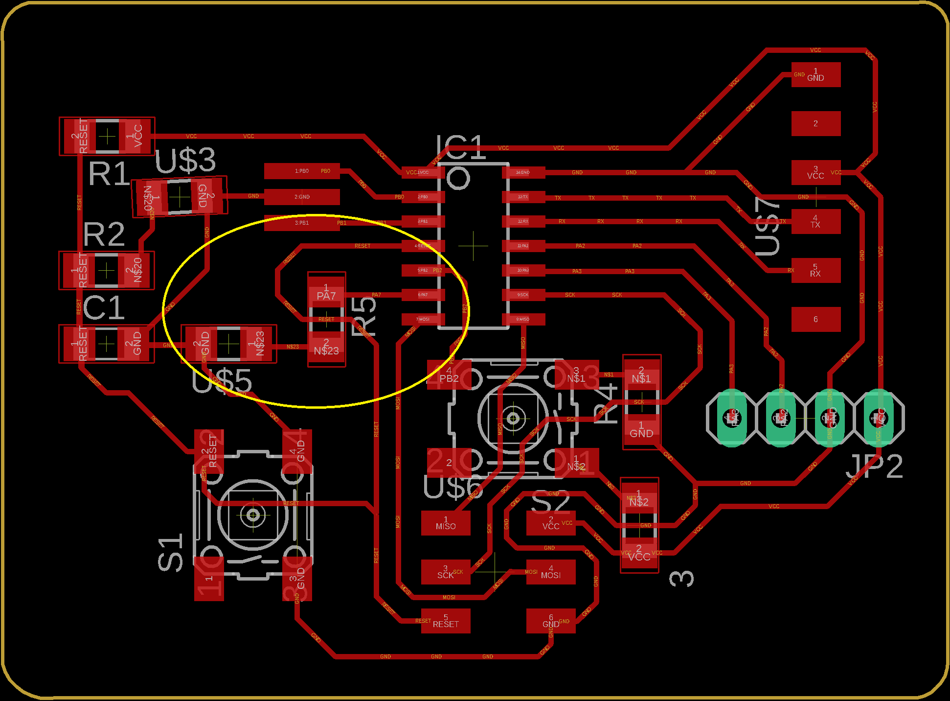
I used my helloworld board for this week i.e.'Embedded Programming'. I had already added 1 LED and that LED connected to the digital pin 'PA7' of Attiny 44 uC. As shown in below:
Programming [Arduino IDE]:
I used Arduino IDE For Programming.
The Arduino integrated development environment is a cross-platform application that is written in the programming language C++. It is used to write and upload programs to Arduino board.
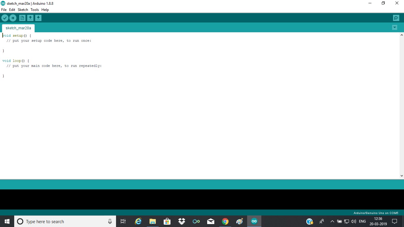
This is first window of Arduino IDE:
Adding Amtel uC to Arduino IDE:
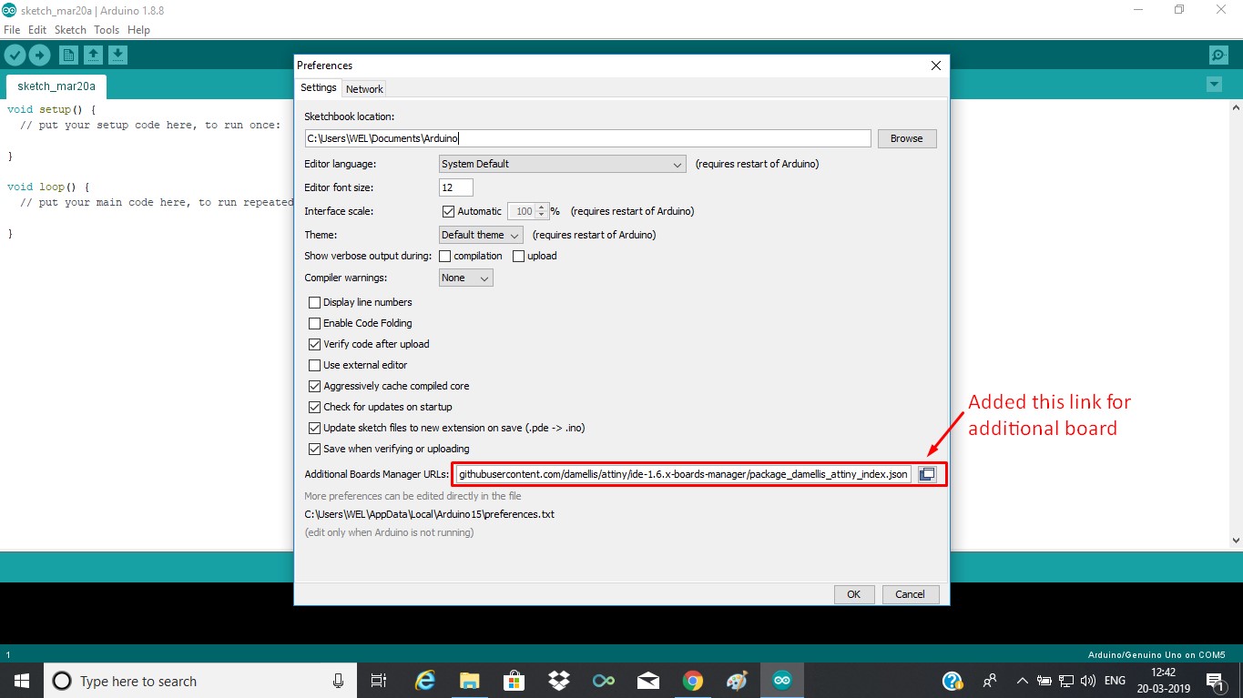
I had gone through "highlowtech" tutorial for making arduino IDE as a programmer.
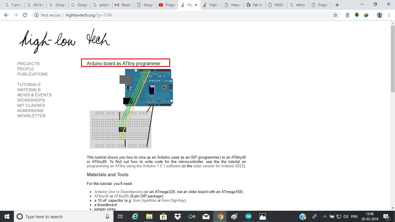
According the above I followed the instructions as follows:
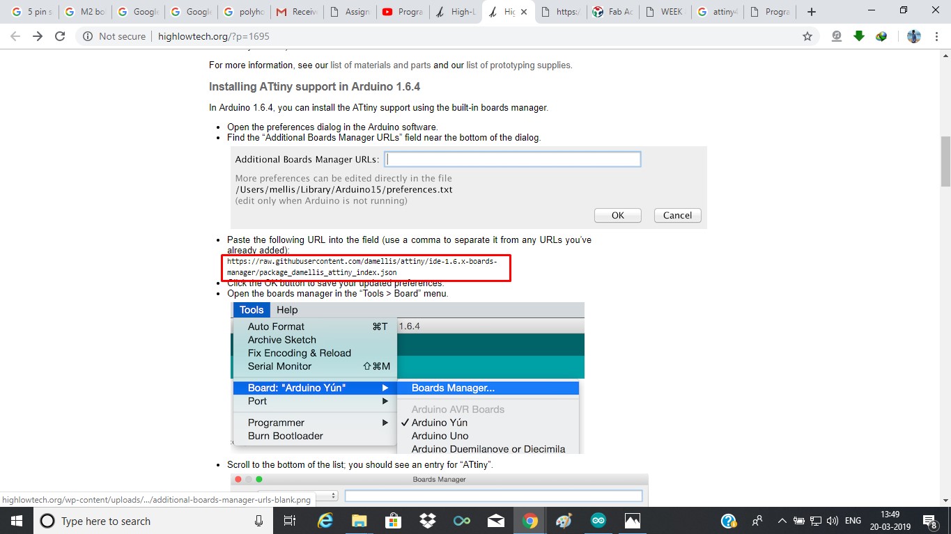
Cpoied above link add on Arduino IDE is shown in following image
Then I added to my Arduino IDE Attiny board package by "David A. Mellis"
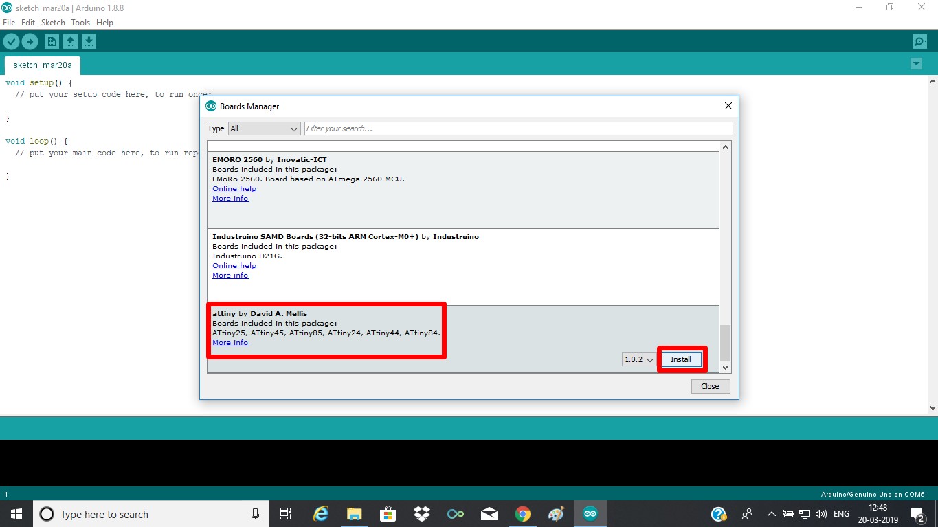
After the installation I saw the 'Tool>>Borad:'. And here I found the Attiny board pacakage were installed successfully as shown in below:

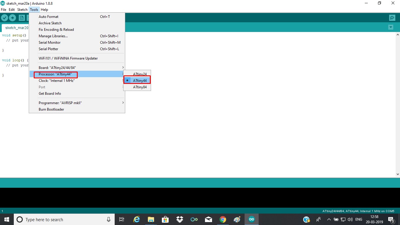
Then, I need to setting the 'Processor' and 'clock' selection for programming.
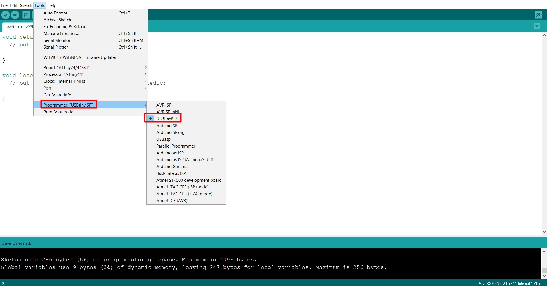
I used Arduino as a 'Programmer', while first time doing programming through Arduino IDE.
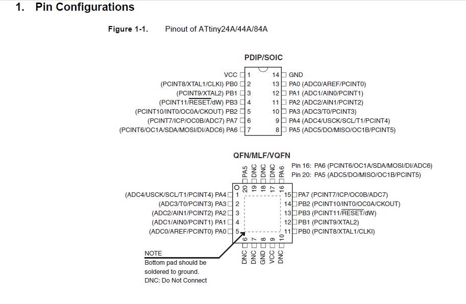
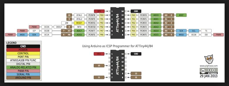
Before going to programming, I need to understand pin-configuration of Atmel uC, when we have to do programming through Arduino IDE.
The pinout diagram of Attiny 44 A is shown in below, Where shows pin numbers for progrmming to my hello board:
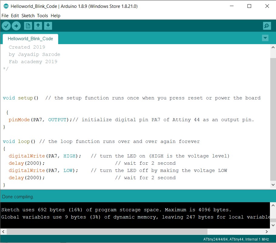
I wrote code in arduino for heeloworld to blink a LED, is shown in below:
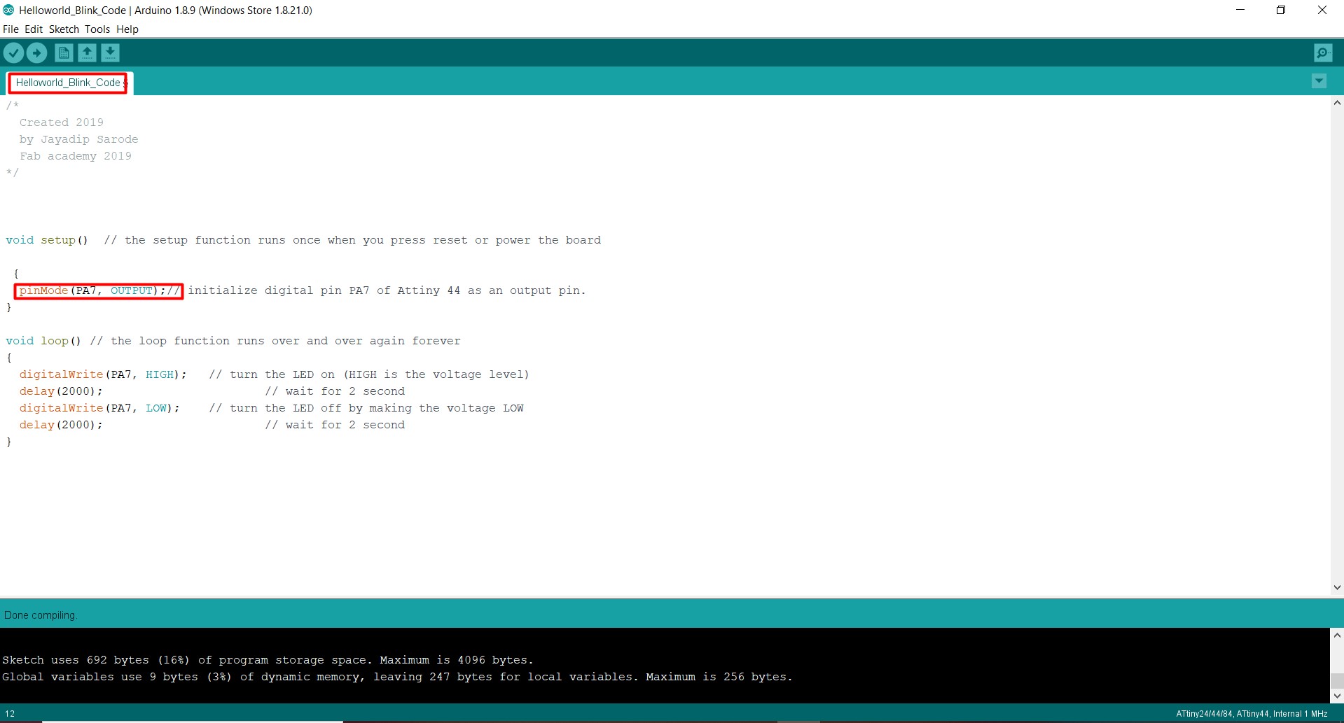
/*
  Created 2019
  by Jayadip Sarode
  Fab academy 2019
*/

void setup()  // the setup function runs once when you press reset or power the board

 {
  pinMode(PA7, OUTPUT);// initialize digital pin PA7 as an output.
}

void loop() // the loop function runs over and over again forever
{
  digitalWrite(PA7, HIGH);   // turn the LED on (HIGH is the voltage level)
  delay(2000);                       // wait for 2 second
  digitalWrite(PA7, LOW);    // turn the LED off by making the voltage LOW
  delay(2000);                       // wait for 2 second
}
Helloworld_blinking a LED, as shown in below:
Learning Outcomes:
1. Learned 'how to add other uC boards to Ardiuno IDE'.
2. Understand uC pinout for programming.