Work flow of assignment
What is PCB...?
Printed Circuit Board
A Printed Circuit Board (PCB) mechanically supports and electrically connects electronic components or electrical components using conductive tracks, pads and other features etched from one or more sheet layers of copper laminated onto and/or between sheet layers of a non-conductive substrate. Components are generally soldered onto the PCB to both electrically connect and mechanically fasten them to it.
Printed circuit boards are used in all but the simplest electronic products. They are also used in some electrical products, such as passive switch boxes.
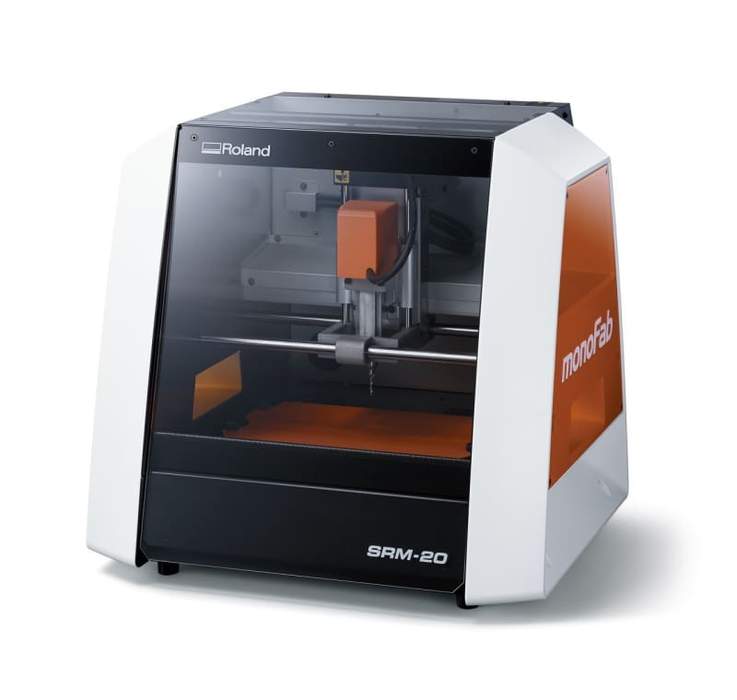
About Milling Machine(SRM-20):
SRM-20 can bring shape to virtually any idea that springs to mind. With the SRM-20 3D milling machine, 3D data can be shaped into solid objects with exceptional precision. Capable of milling a wide range of materials, the SRM-20 is invaluable for industrial design prototypes, industrial parts, educational tools and other applications using materials similar to the final version. Its desktop size means it can be used almost anywhere, while the bundled software suite makes operation easy, even for beginners.
In our fablab have "Ronad SRM-20" Milling Machine. SRM-20 have more features than the MDX-20. like user-define origin etc. Now I am going to mill my pcb and make the group assignment.
Group Assignment:
We characterised the design rules for our PCB production process.
Line Test: Me, Tushar Kukreja and Manoj Sahukar teamed up for the assignment.
A. The line test images were taken from Fab Academy Electronic Syallbus.
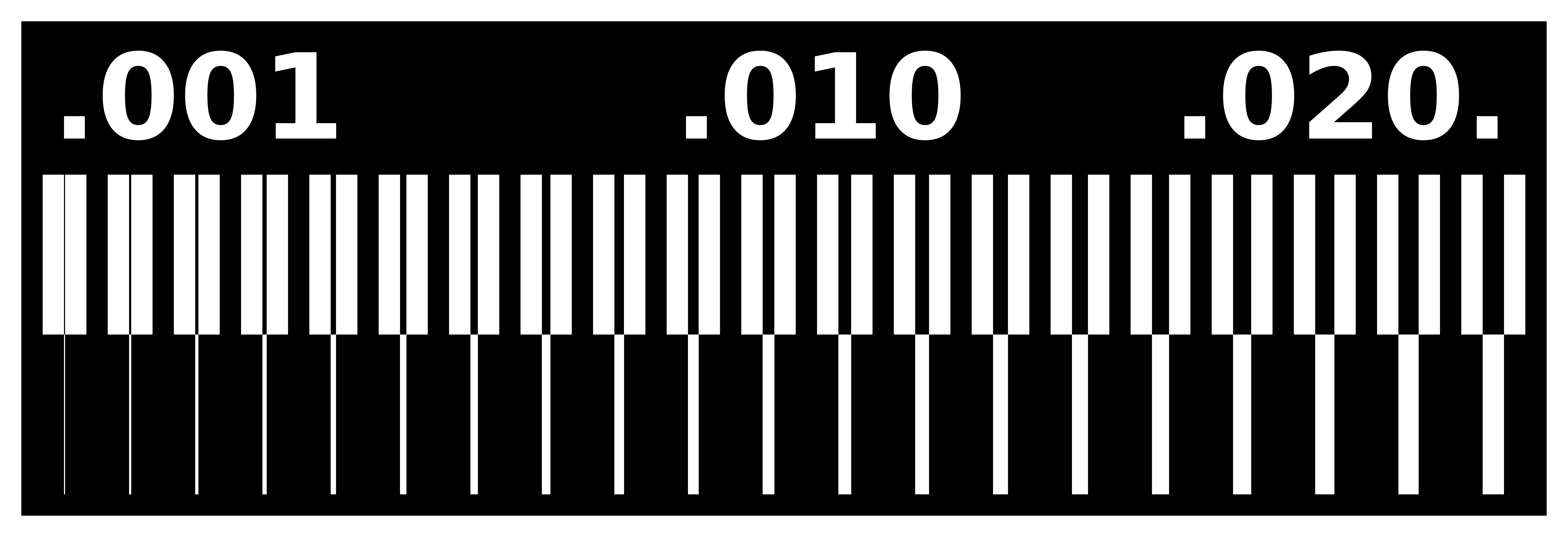

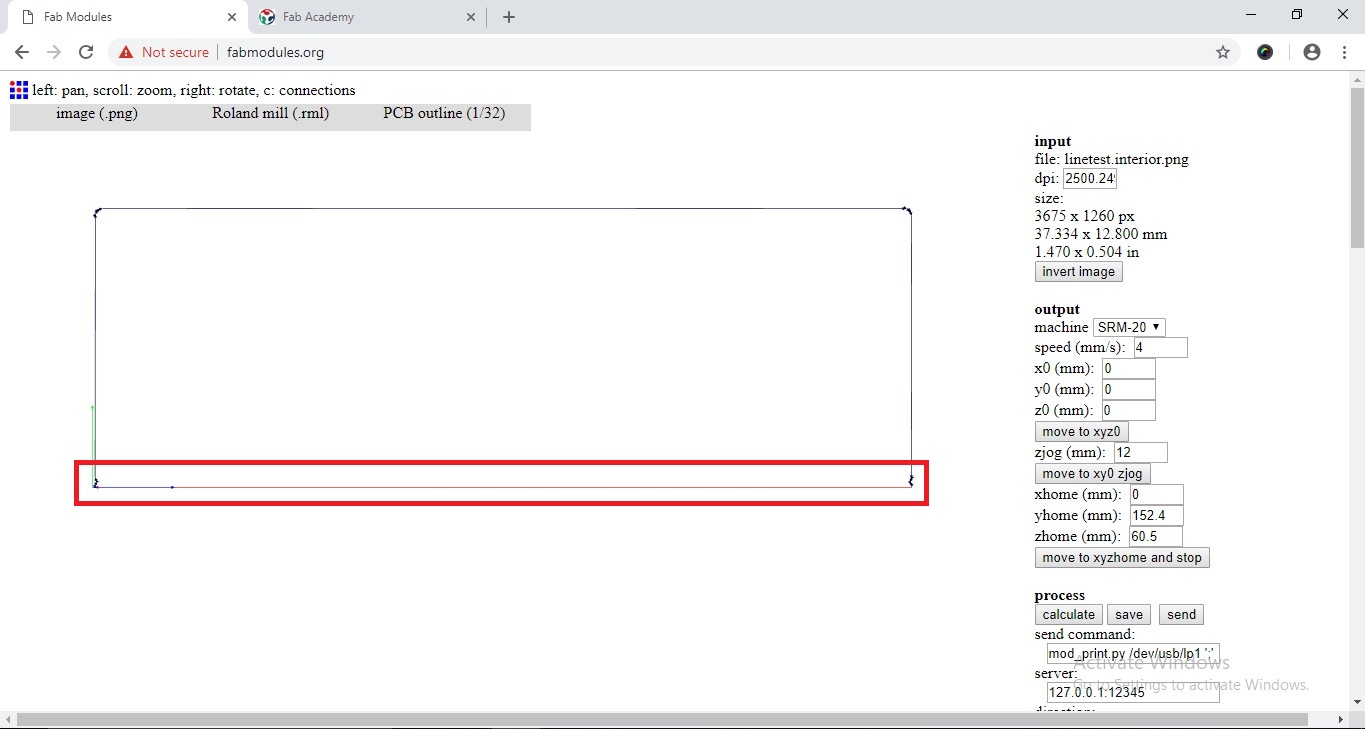
B. We used Fab Modules to generate .rml files. Various other settings like process,speed,X,Y,Z coordinates were entered.
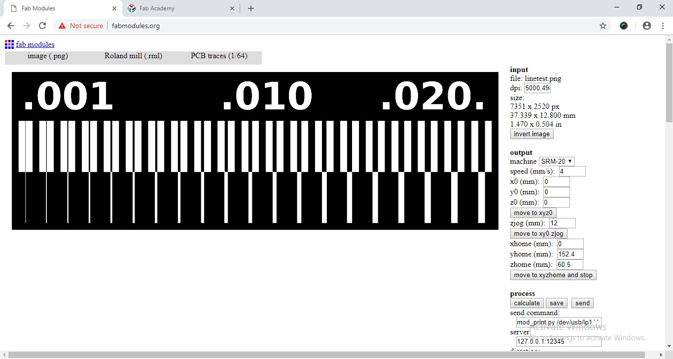
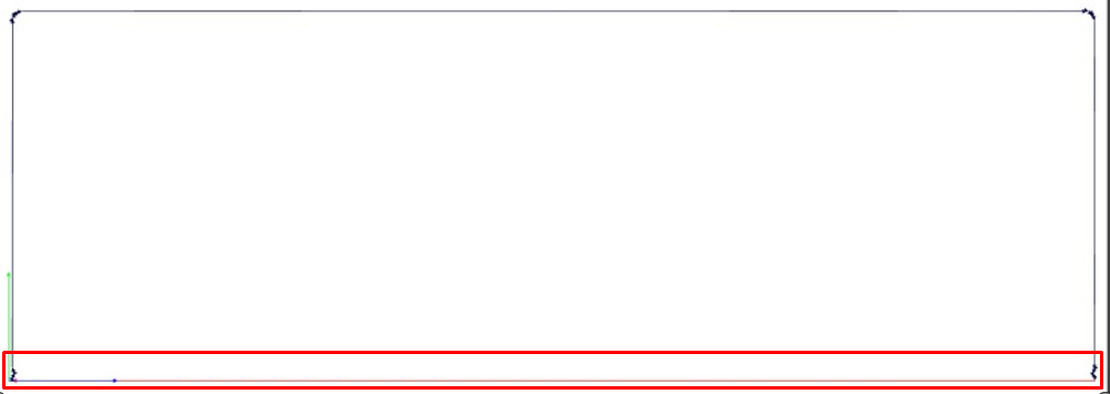
C. There was 1 line of the reactangle Red which showed jog path. The FabModule didn't create close rectangle which can be seen in the picture below.
D. We cut the board on SRM-20 machine. Gave 2 commands to trace the lines of various thickness and cut the outline.
F. Problem:
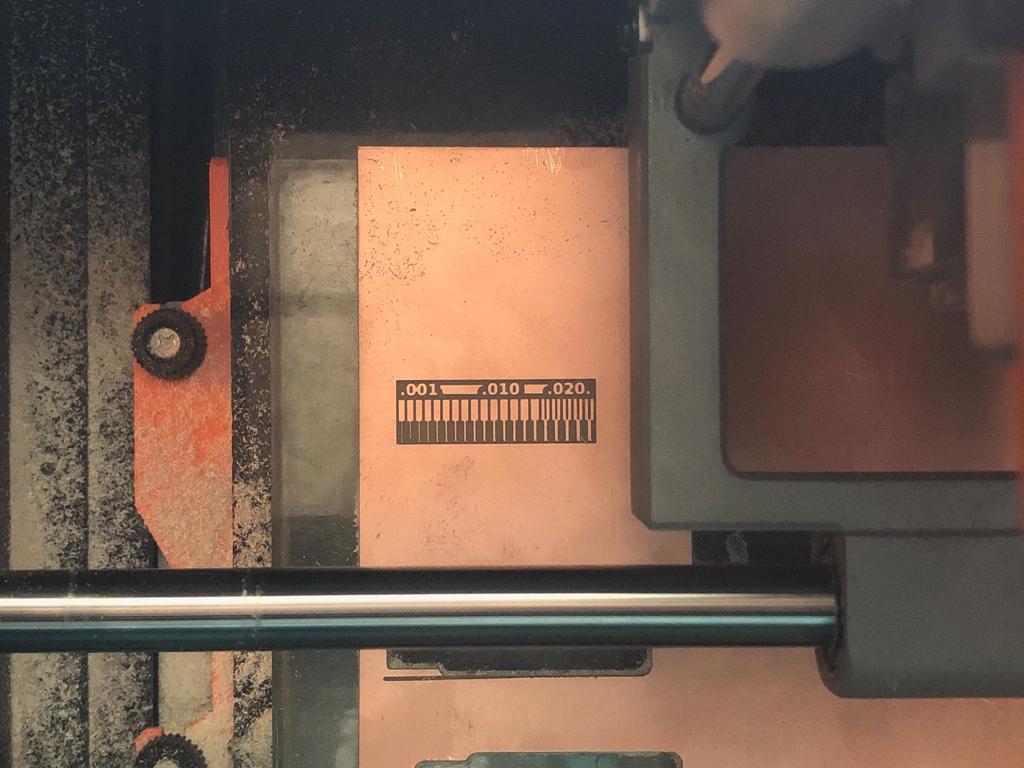
The board wasn't cut from one side because the path only showed way for 3 sides of the rectangle. Though the input image(.png) had a close rectangle, on 'Fab Modules' in path 1 line of the rectangle was Red and showed jog path.
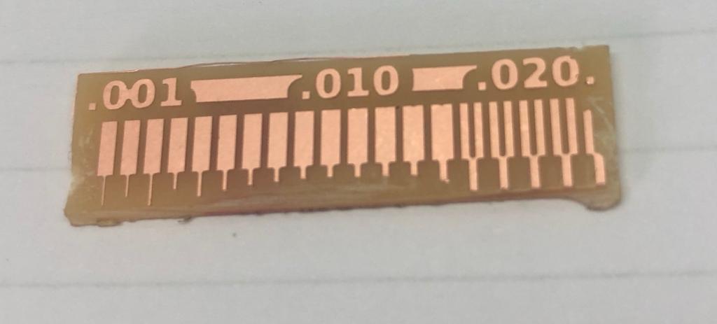
To fix this problem, we cut the 4th side of the board with grinding machine. This damaged the board little bit yet the test part was clearly visible.
We also reversed the rectangle outline design to get path on the 4th side and again calculated the path. Yet fab modules gave the same result showing the same 3 sides for cutting. Moreover, during the lecture we realized the same problem of machine not cutting the 4th side of the rectangle was also faced by other labs. Yet the assignment was done successfully as the traces were clearly visible.
E.Conclusion:
The board showed the smallest thickness line was cut prperly. Thus, giving green signal for the tracing and outline ahead.
Individual Assignment:
PCB Frbrication:
Neil introduces various ways to make our 'Fabisp'. Sean, Alex, Tomás, Jonathan, Brian & Zaerc these guys done using ATtiny45 and Ali, Valentin, Bas, Andy & David these done using Attiny44.
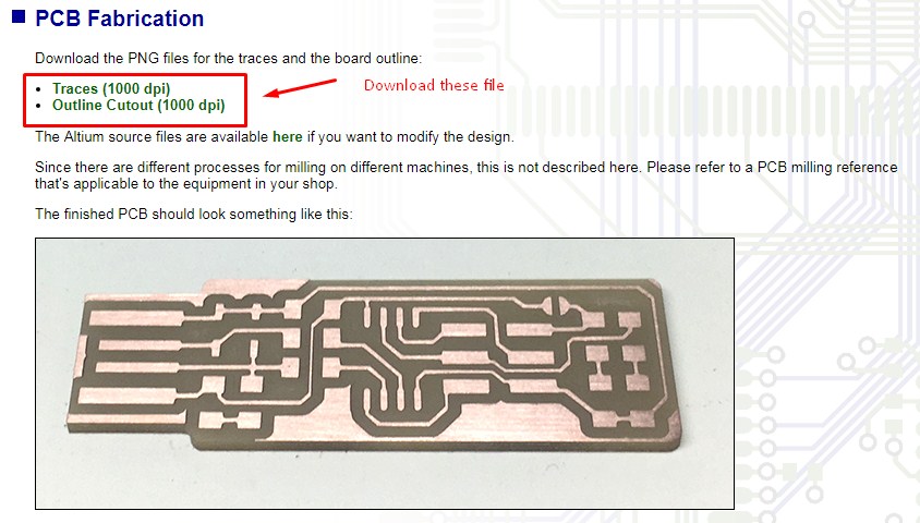
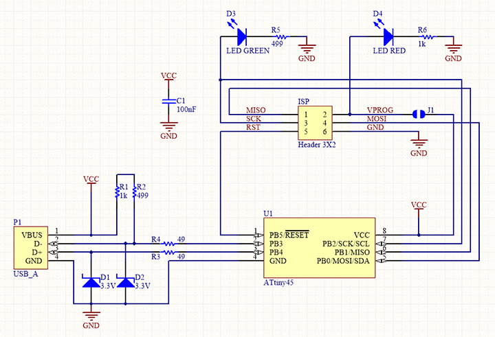
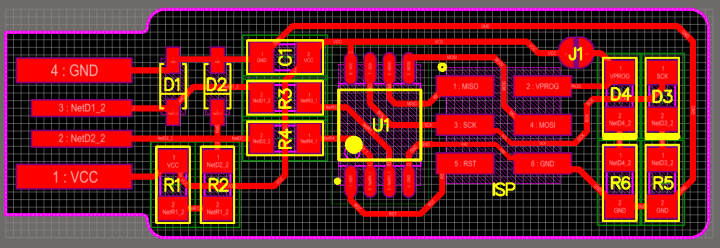
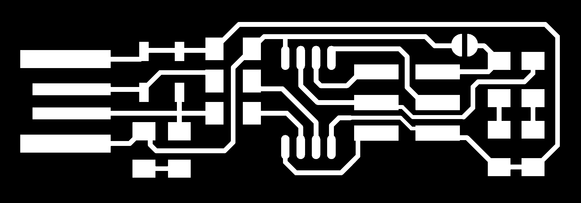
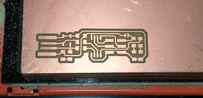
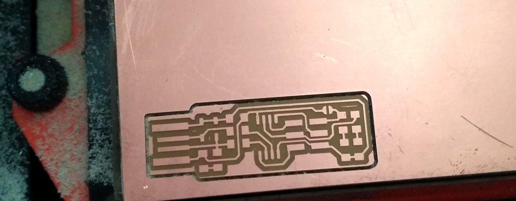
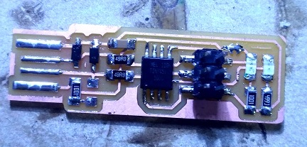
I choose the Brian's Board to mill my PCB. So i downloaded the '.PNG' file of "Board traces" and "Outline".
Schematic of Brian's board is shown as below:
PCB board of Brian's board is shown as below:
Monochrome image of pcb traces resolution is '1000 dpi'. The image is shown as below:
Monochrome image of outline resolution is '1000 dpi'. The image is shown as below:

Fab Modules:
The fab modules provide a set of software tools for personal fabrication, intended for use with machines common to fab labs.
It includes:
1.Tools to design 2D and 3D objects.
2.Functions to generate 2D and 3D toolpaths.
3.GUIs workflow from design files to machine commands.
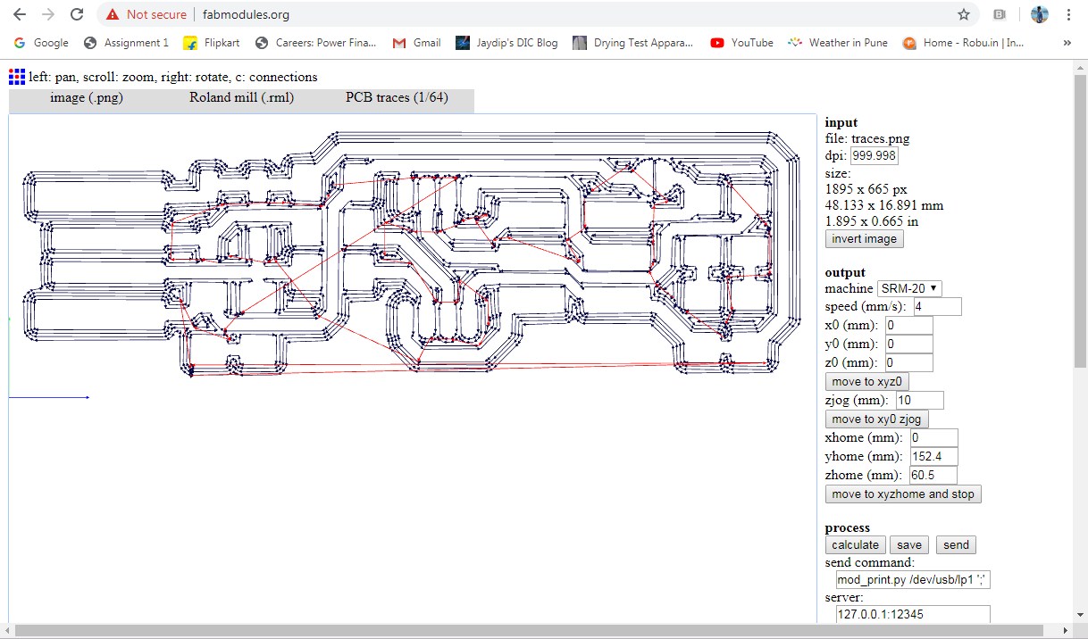
To make '.rml' file of pcb traces from monochrome PNG image, using 'Fab modules'.
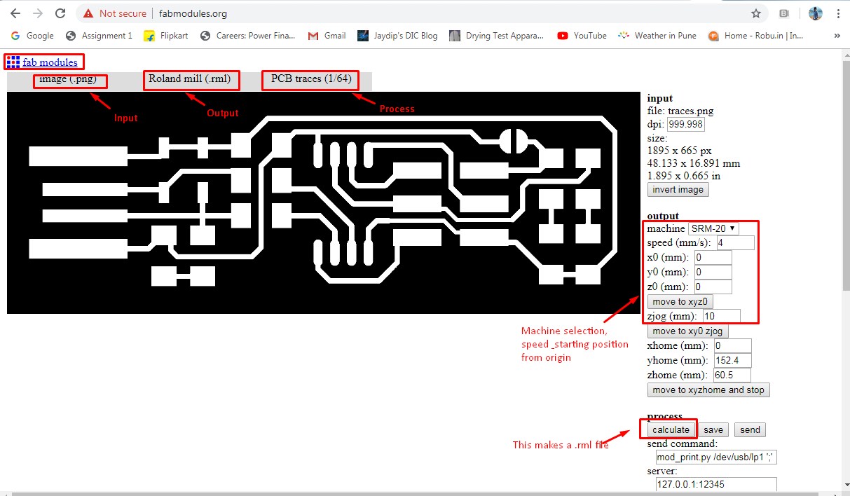
After clicking 'Calculate' opton, then created a toolpath. Then save the '.rml' file of traces.
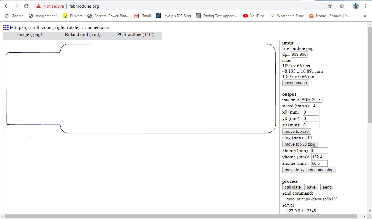
To make '.rml' file of pcb traces from monochrome PNG image, using 'Fab modules'.
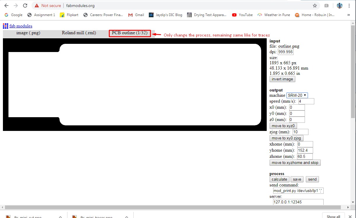
After clicking 'Calculate' opton, then created a toolpath. Then save the '.rml' file of outline.
About Vpanel software:
Then I went for milling on SRM-20 machine. 'Vpanel' is machine software for SRM-20. So firstly I need to learn about 'Vpanel'.
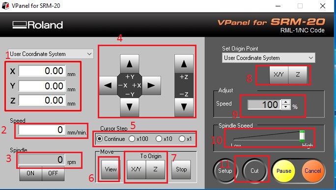
1. Use Coordinate System:
When we moves X,Y and Z postions, we get cordinations here.
2. Speed:
It shows speed making traces in 'mm/min'.
3. Spindle
It shows spindle speed in 'rpm(revolution per minute)'.
4. Moving system
Using these buttons we can move the cursur position X+, X-, Y+, Y-, Z+ and Z-.
5. Cursur Step
Selecting below options we control the speed of cursur's steps.
6. View
When we click this option, machine will pause and bed comes outside.
7. To Origin
When we set our coordinates, then when we click on 'X/Y' and 'Z' machine cursur comes at point, where we set our coordinates.
8. User Coordinate System
When we moves the cursur manully, then by clicking these buttons we can set our coordinates as aorigin.
9. Speed Adjust
Using this we can adjust speed of making traces.
10. Spindle Speed
Using this we can Increase or decrease speed of Spindle motor.
Before starting milling taces, I fitted '1/64' bit in machine's collet. I had set the gravity on the machine and then make the X, Y and Z coordinates zero, called as a setting origin.
Then going to cut my file. So opened 'cut' option and a '.rml' file. Then select the file and clicked on 'output', then machine Started milling traces.
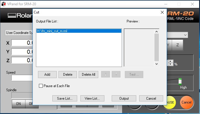
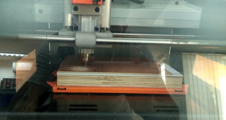
After completing milling traces, I changed the bit 1/64 to 1/32 fot cutting outline. And done again gravity setting.
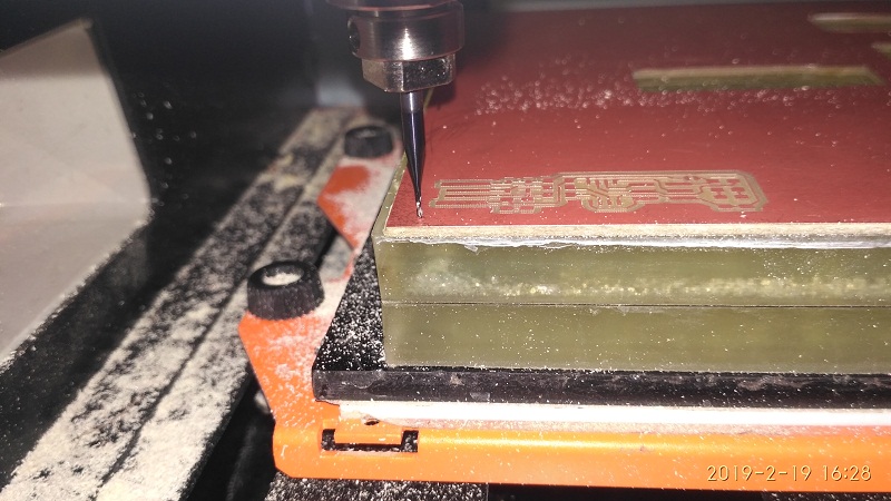
Outline cutting is done successfully.
Soldering:
Soldering is the process of joining two or more electronic parts together by melting solder around the connection. Solder is a metal alloy and when it cools it creates a strong electrical bond between the parts.
After completed milling of my board, then I went for soldering. So I needs following components.
1 x ATtiny45
2 x 1kΩ resistors
2 x 499Ω resistors
2 x 49Ω resistors
2 x 3.3v zener diodes
1 x red LED
1 x green LED
1 x 100nF capacitor
1 x 2x3 pin header
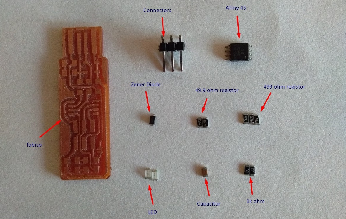
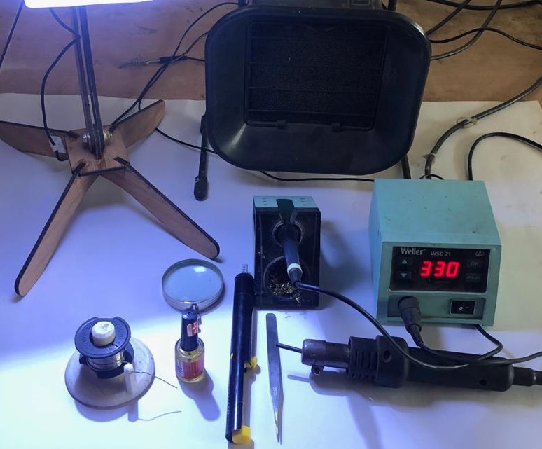
I done the Soldering in only one attempt successfully. Then I need to programme it.
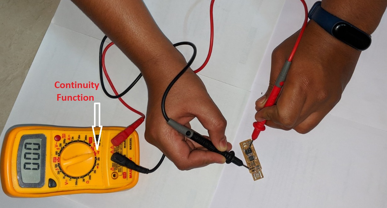
Testing:
The PCB test of a board will use capacitance and resistance. A capacitance test will test for opens and shorts by sending a charge on the trace and then probe each net to measure the induced capacity. Resistance test measures resistance as the current flows through a conductor/trace, in ohms. Also checked continuity between soldered components and tracces by using continuity mode on multimeter is shown in below:
FABISP Programming:
Programming is the process of taking an algorithm and encoding it into a notation, a programming language, so that it can be executed by a computer. Although many programming languages and many different types of computers exist, the important first step is the need to have the solution.
I done programming by followed
Brian's programming documents.
Install the Atmel GNU Toolchain
I download the Atmel AVR Toolchain for Windows from Atmel's site and run the installer. When asked where to extract the files, click the "..." button and navigate to C:\Program Files, then click Extract.
Install GNU Make
I Download Gnu Make and launch the installer. Accept the default location for the installation.
Installation avrdude
I download Avrdude and extract the zip file. Then extracted file copy and paste in 'C:\Program Files'.
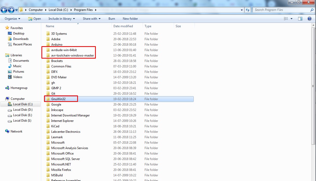
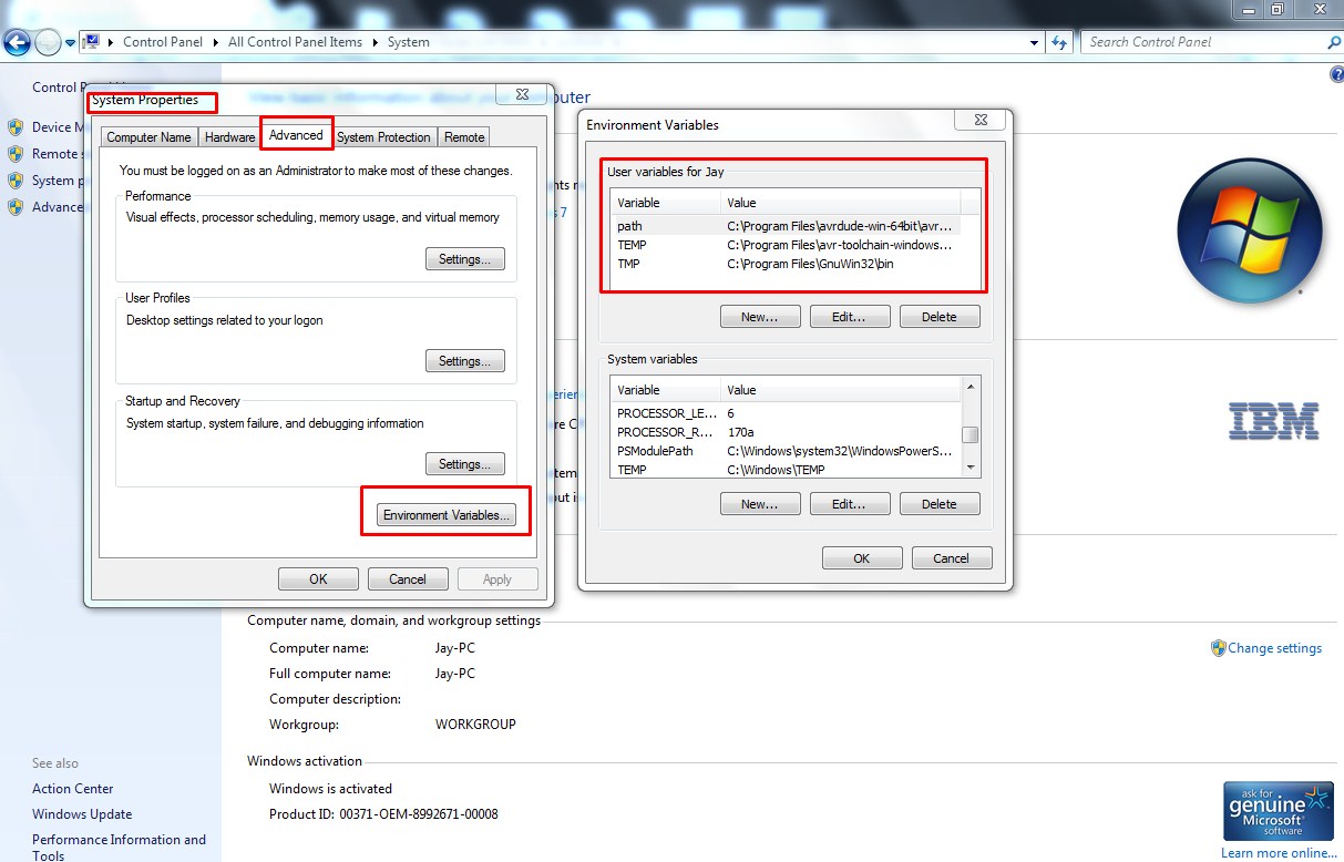
Updating Path
I opened the Control Panel, then go to System. choose "Advanced System Settings". Under the Advanced tab, click the "Environment Variables" button.
I don't already have a variable "Path", so click the New button to created it, entered "Path" without the name.
The three values were added as follow:
C:\Program Files\avr8-gnu-toolchain\bin
C:\Program Files (x86)\GnuWin32\bin
C:\Program Files\avrdude
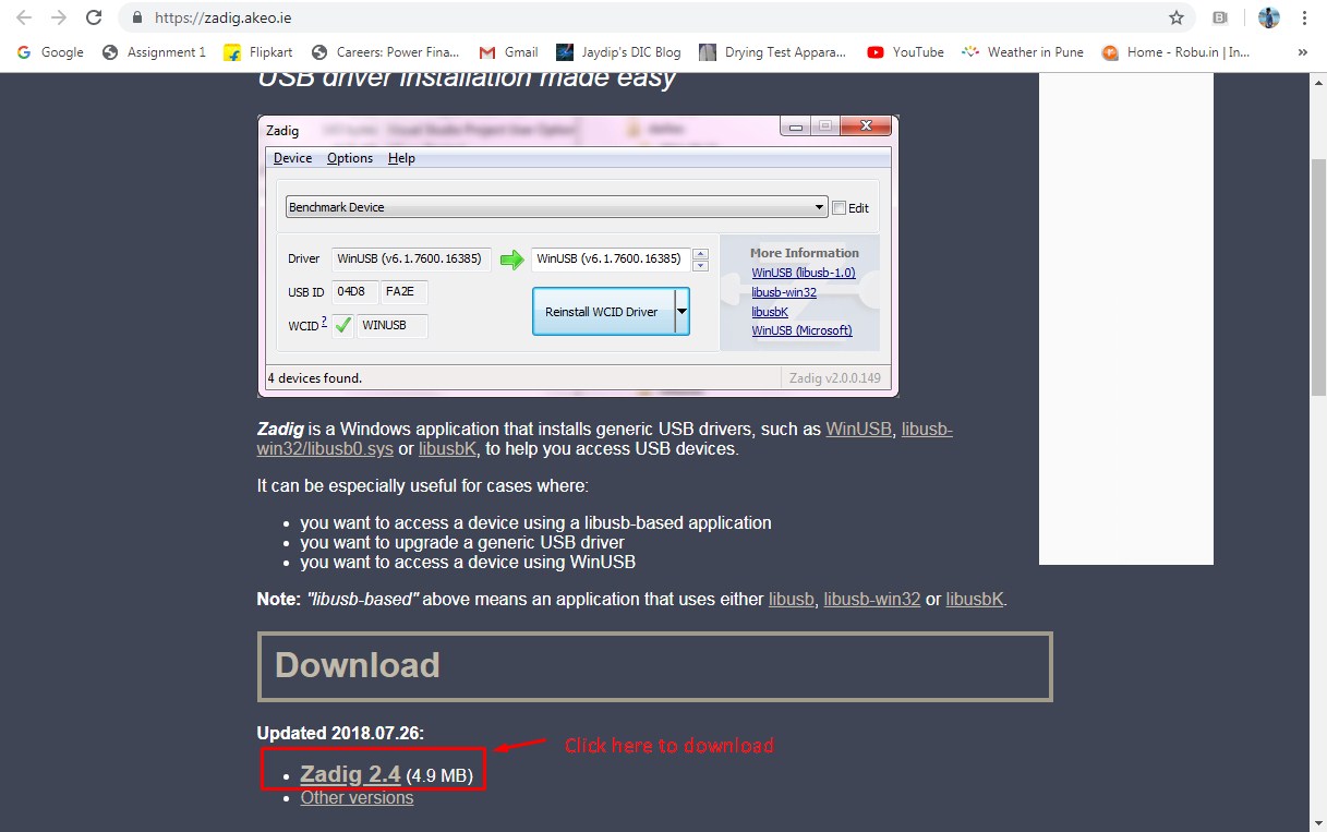
Installing drivers for FabISP Programmer
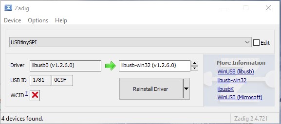
I programmed my FabISP board by another 'FabISP Programmer' using 'Zadig' software. Zadig is a Windows application that installs generic USB drivers.
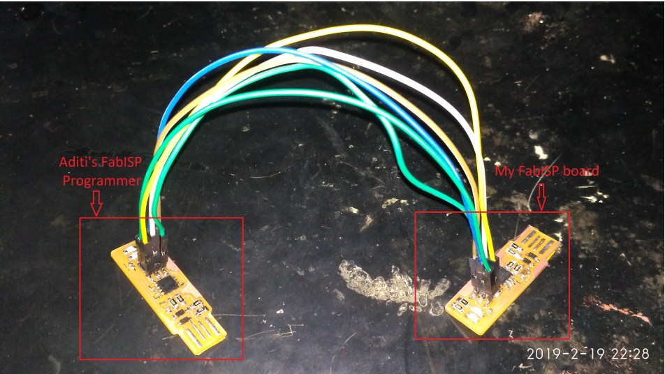
So, I download Zadig and launch it. Then I connect Miss_Aditi's 'FabISP programmer', and select the "USBtinySPI" device in the list.
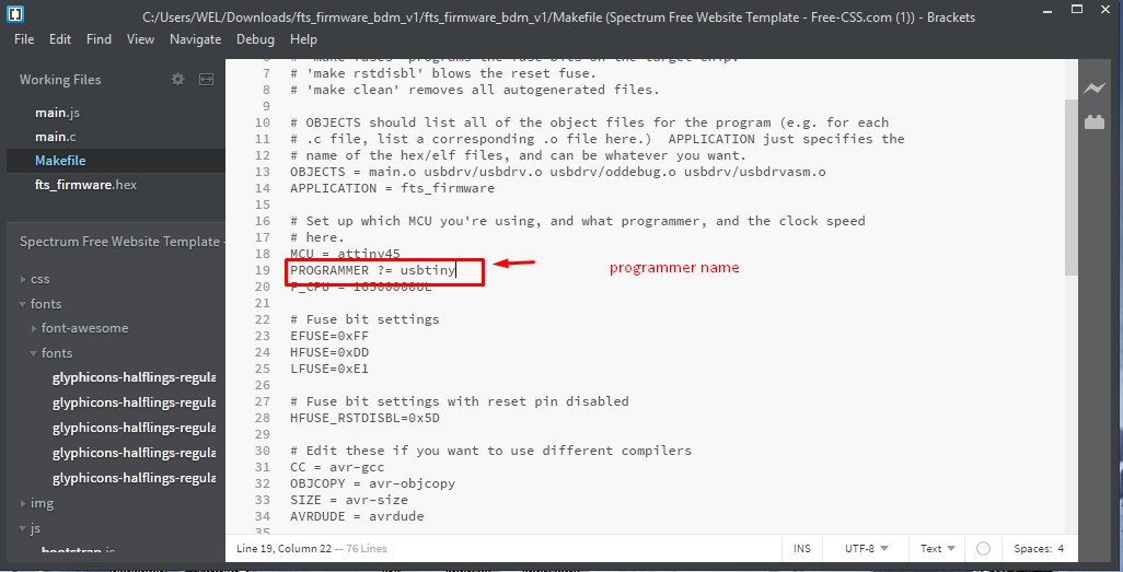
Before the Programming we need to edit "Makefile". Because there is a need to set your programmer name. e.g. usbtiny, etc.
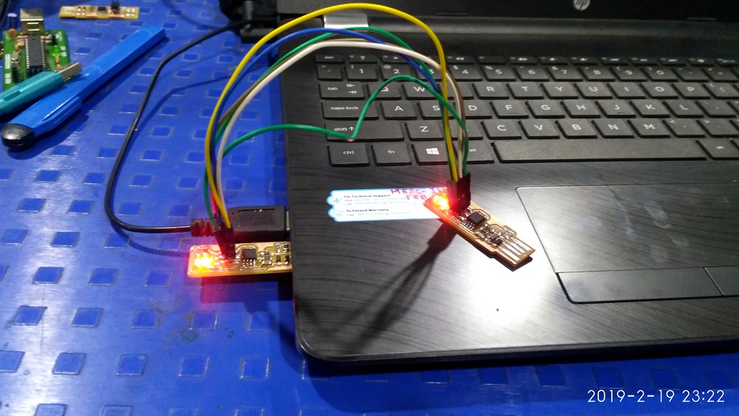
Before the Programming I did connection using jumper wire My board to Aditi's FabISP Programmer.
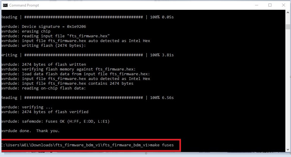
I run the folling commands:
1. make flash
Using this command I burned the program in my board using another Fab_ISP.
I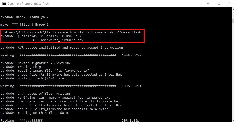
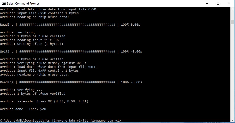
2. make fuses
Fuse memory is a seperate chunk of flash that is not written to when you update the firmware.
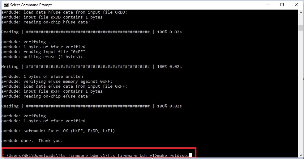
3. make rstd
Using this command I did the my borad permantent programmer as a Fab_ISP Programmer.
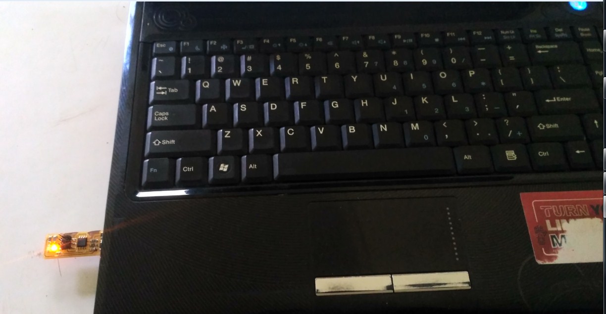
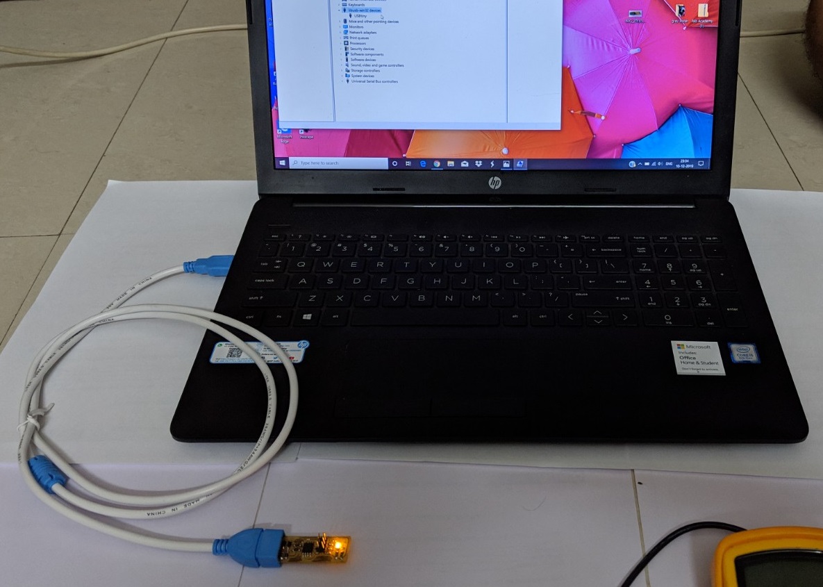
Testing:
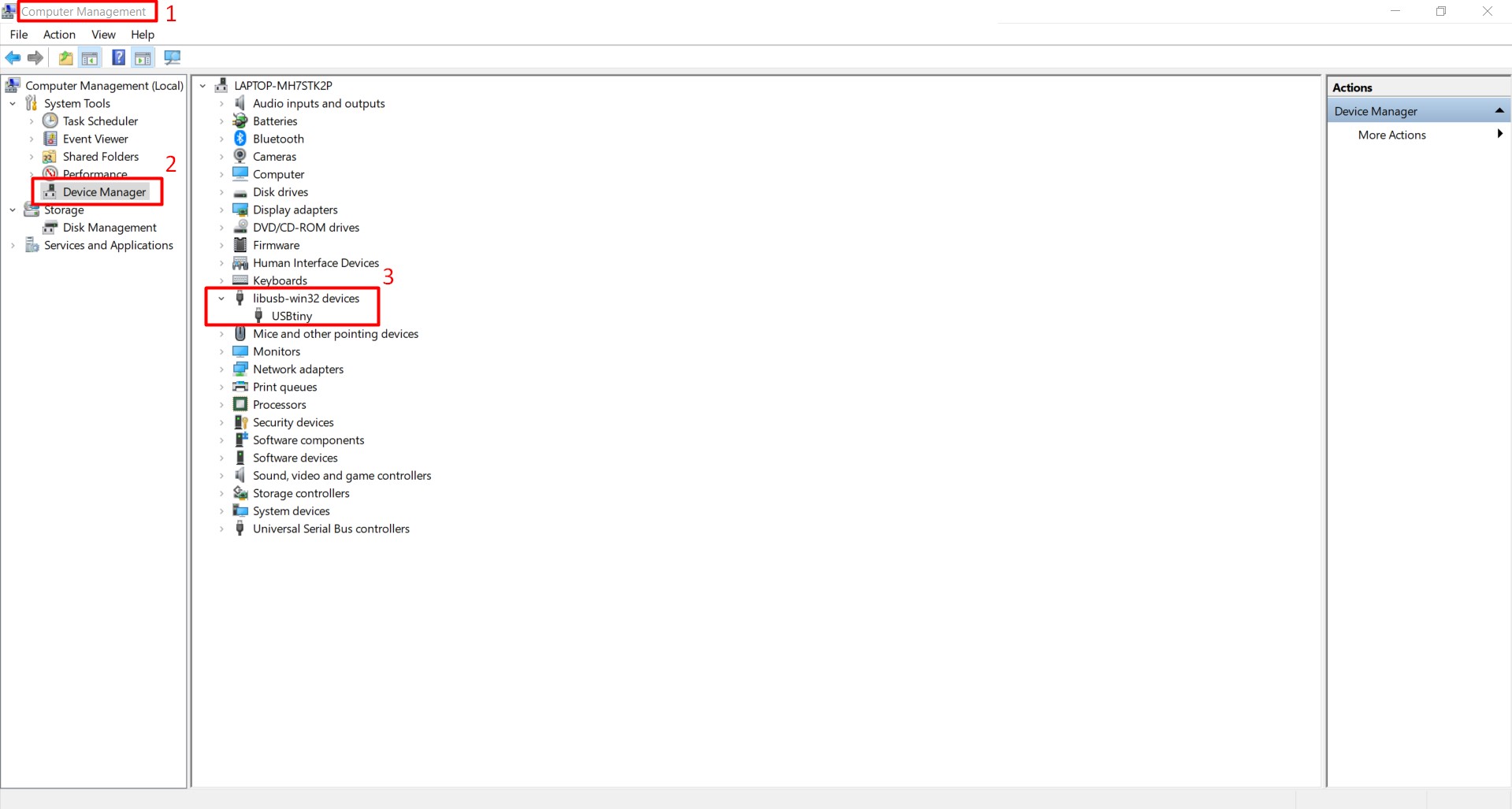
After completing the burning process, I checked my Fab_ISP Programmer by connecting to my Laptop using Male-Female USB cable. Then I checked in Computer management>Device manager>libusb-win32 devices as shown in following:
Learning Outcomes:
1. Learned operations of 'SRM-20' Milling machine.
2. I did fist time SMD component soldering.