Week 7. Electronics Design
Go to:
1. Group Work
Small time shift, because the group work was done after the individual assignment.
Task: Use the test equipment in your lab to observe the operation of a microcontroller circuit board.
Group:
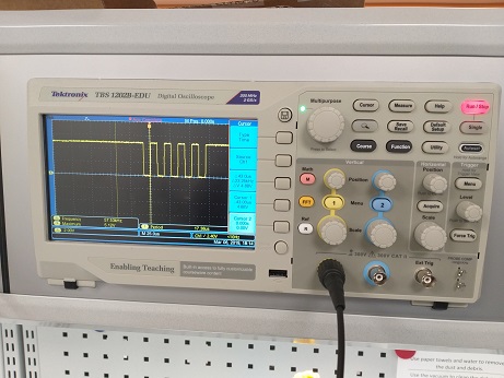
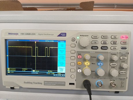
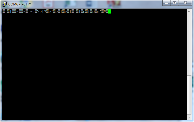
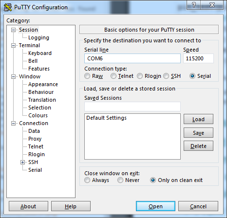
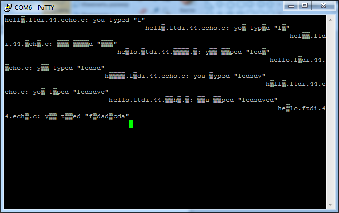
We had a Hellow Word board, oscilloscope, FTDI cable and PuTTY terminal, opened in serial mode on 115200 BPS.
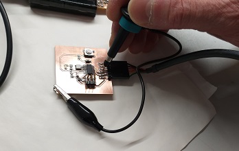
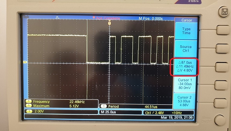
Typing a letter on a keyboard, you can see the binary format of the letter on the screen of the oscilloscope. Without any preferences, we typed a few random letters: "U","S" and "B"

2. Hello World Board
Tasks:
 Redraw the echo hello-world board
 - Add (at least) a button and LED (with current-limiting resistor)
- Check the design rules, make it, and test it
I started working on this weeks assignment by downloading Eagle from official web page. Another new software for me. A long time ago in galaxy far far away I was using P-CAD but this knowlege didn't helped me at all. After installing Eagle I downloaded eagle_fab.lbr and put it into libriries folder.
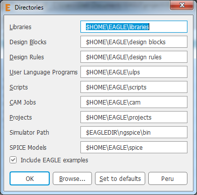
After that eagle_fab can be found in libraries list. I enabled it by Right Click on it and put a tick in the regiment Use . Then I created a new project and named it ElectronicsDesign_FabAcademy. Then I created a new schematic (Right Click on project name New/Schematic).

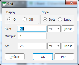
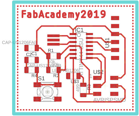
In Scheme1 file I started redrawing Hello World Board. Before start I turned on Grid for better positioning. I opened thisPNG and started adding components to the sheet. To add an element to the sheet I typed add in command line (there's an add tool on the tool panel as well). In Add window you can choose a component from the libraries. From eagle_fab library I added:
- ATTINY44-SSU
- RES-US1206FAB (1206 - dimensions of the component. RES - resistor)
- CAP-US1206FAB (CAP - capasitor)
- CAP-US1206FAB (CAP - capasitor)
- RESONATOR 20 MHz
- AVRISPSMD - 6pin connector
- J2 FTDI 1x06SMDHEADER

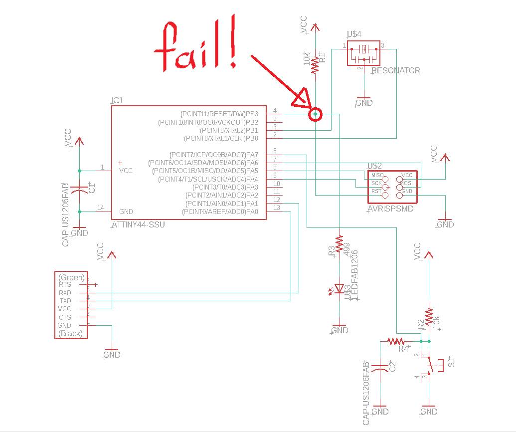
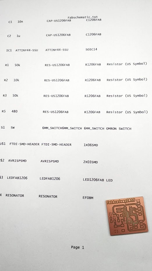
Using Name and Value tools I named the elements ans defined values of the components. I connected components following the paths on the drawing using the Net tool and after that I added ground, button, few resistors and LED. I connected them as well and I did it wrong! It happened that I accidentally connected the LED to PB3 pin instead of PB2. I haven't realised it on the design stage, so I milled the board an only when I started soldering I found the mistake. I soldered the board anyway, but I made another one later.
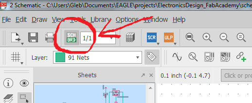
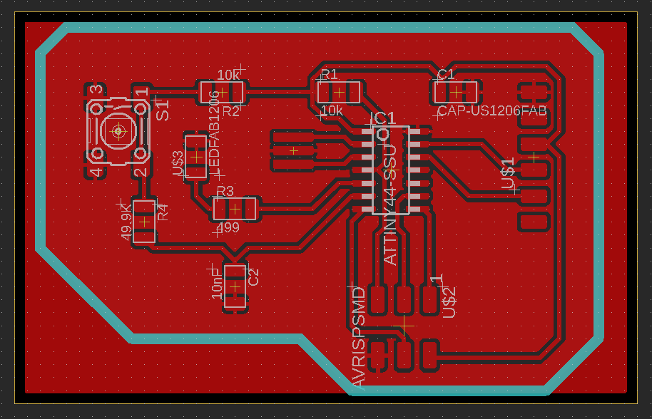
Anyway, after plasing all components and connecting them I switched to board mode. For me it was the most time consuming part.
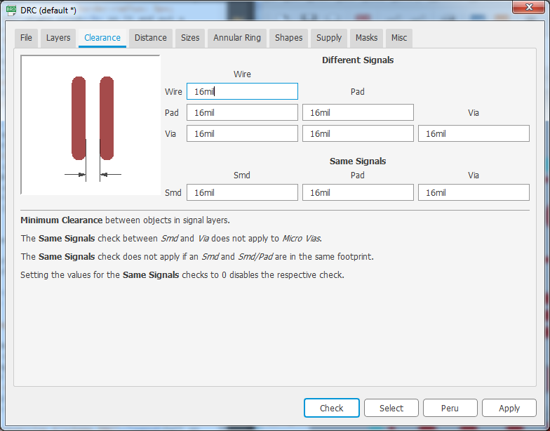
I was trying to place all components in a nice compact way so the paths won't cross. To move an element I used Move tool (click on the cross to select, RMB to rotate). To make a connection between contacts I used Route tool wtith width 16 mil. Using Polygon tool I draw a frame around my design and Named it GND. It is my ground signal. Ratsnest tool connects everything to it. After drawing a path or moving a component it doesn't refresh so you need to press it again. To remove it type ripup GND in command line. After plasing all elements and drawing all paths I checked if my drawing fits my design rules. To do it I typed drc in command line. In this window I defined design rules and clicked apply. The program found a few things like unconnected routes and components placed too close to each other. It was easy to fix it all.
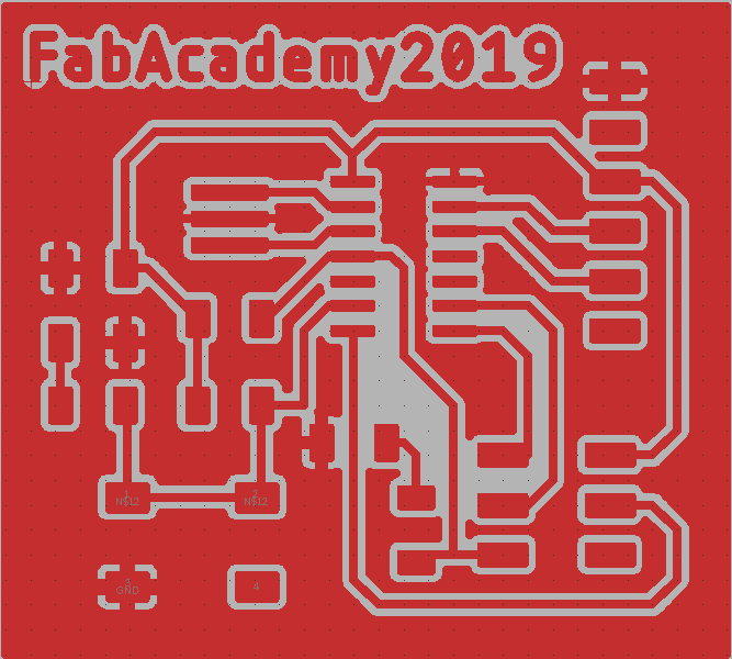
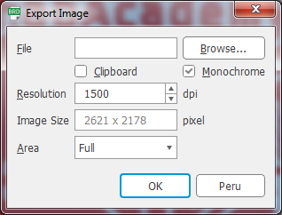
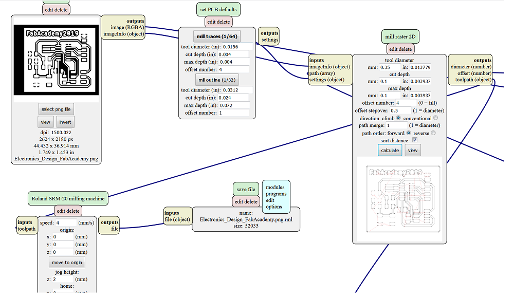
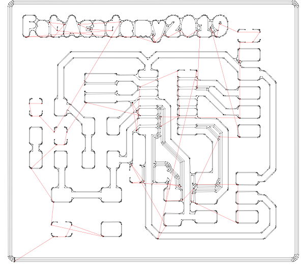
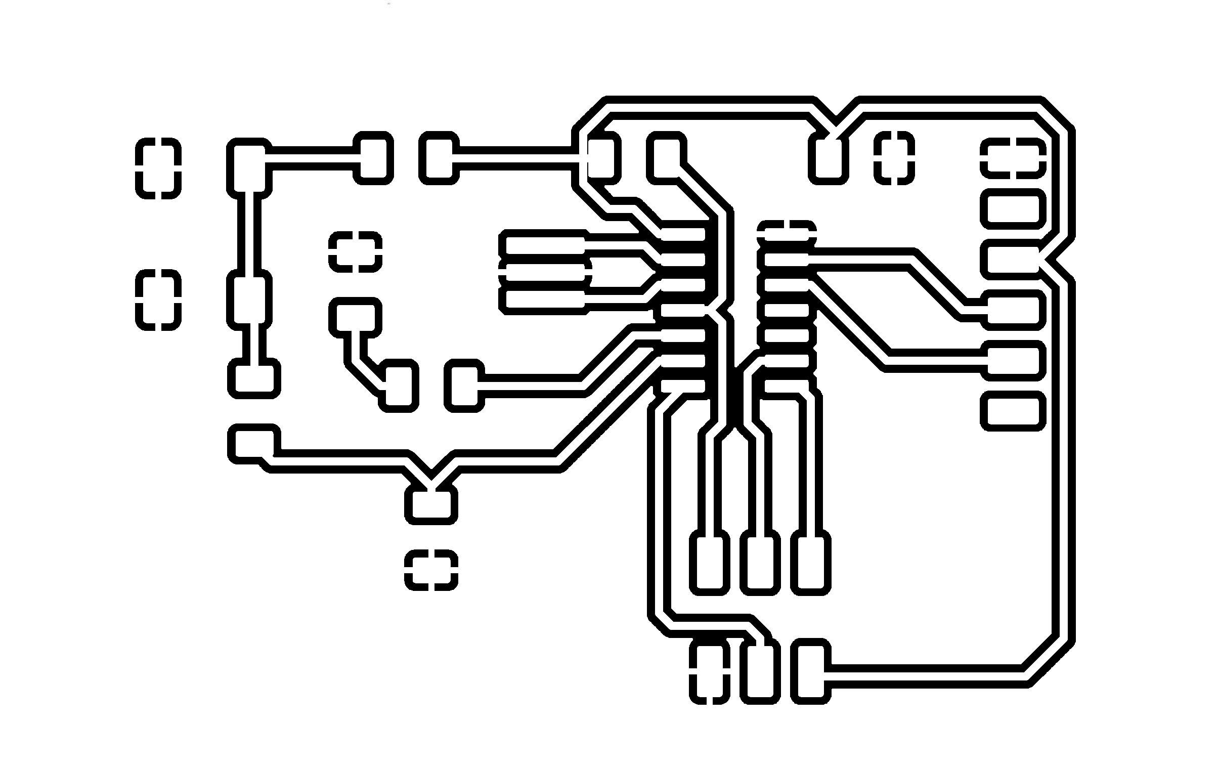
I drew a frame around my board in 46 milling layer using line tool and exported two PNG files: traces and outcut. To export only needed layer type in command line:
display none - hides everything
display 1 - showes only layer1
display all - shows everything

|

|
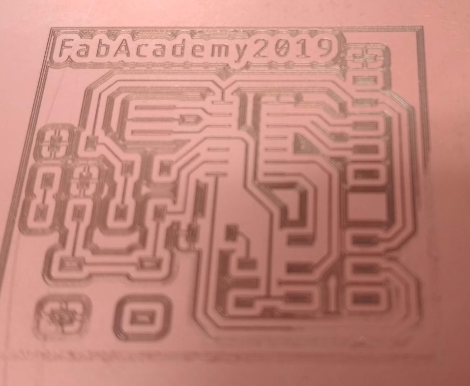
To mill my board I used the same process that I used on week 5. I downlaoded my PNG file to Mods, opened server program SRM-20/PCB PNG, deleted WebSoket module and added file/save module. I used 0.2-0.5mm V-shape milling drill to cut traces and 1mm flat to do the outcut.
|
|
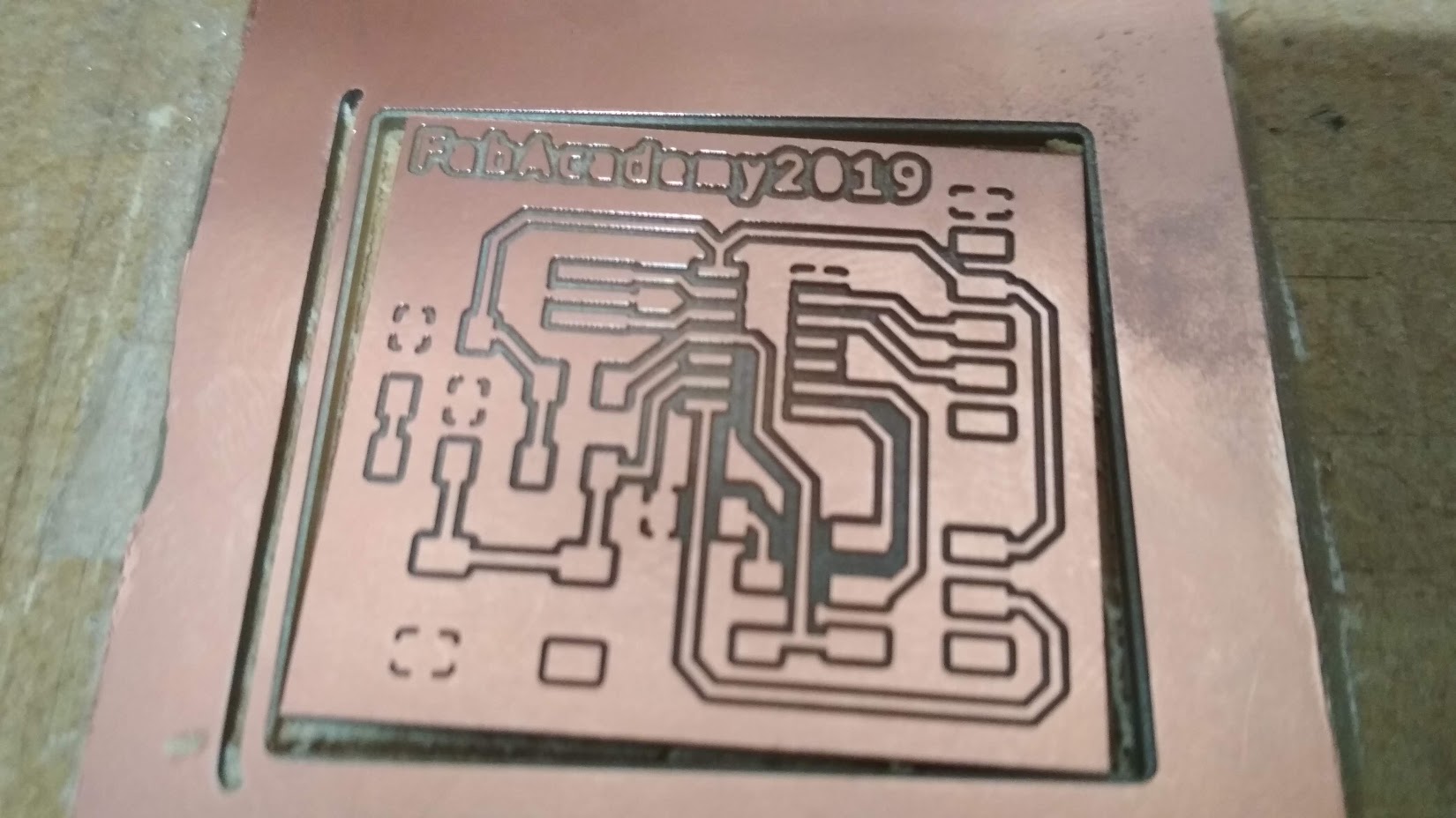
According to my design I did soldering right. According to what was needed it's wrong...

|

|
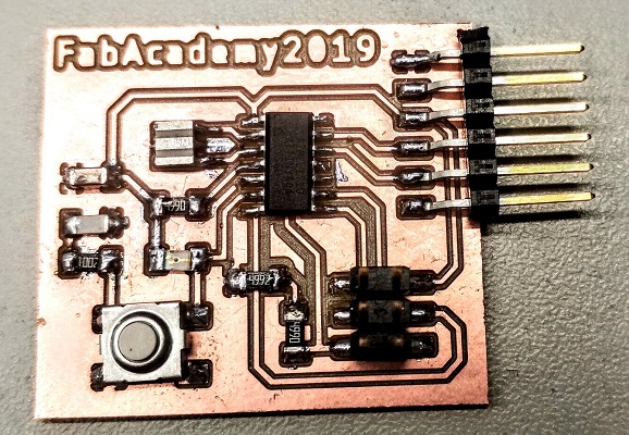
I milled the correct board, using the similar settings that were shown before. I soldered all components and started programming the board.
Programming the board
To program my board I used my version of Brian's programmer. I plugged it to USB 2.0 port (I know that it's better to use a extension cable, but I don't have one so everything looked like that). Then I connected the programmer and ISP header on my board with self-made 6 pin AVR-programming cable. Then I powered the board from FTDI-cable connected to usb port.
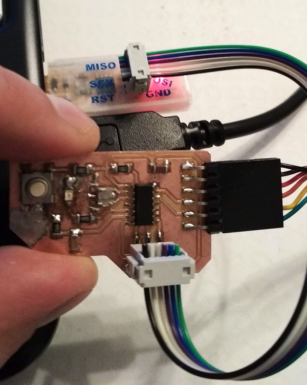
Since my laptop operating on Linux has found his peace in the digital Valhalla, I went through this tutorial to make it work on my Win7 machine.
It wasn't the result I expected, so I started to look for a better easier way to do the programing. And I found it!
I downloaded Arduino IDE and lived happily ever after my life became brighter.
Full tutorial I followed to set the Arduino IDE can be found here
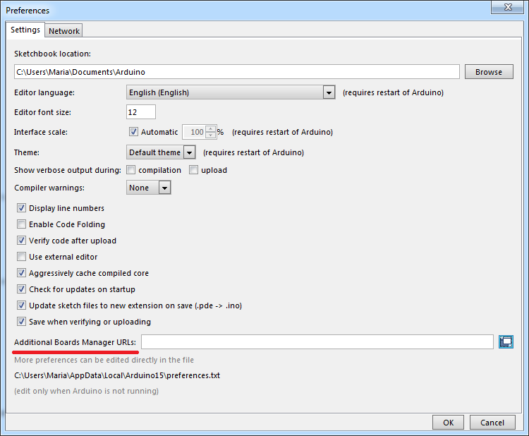
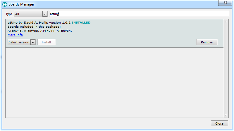
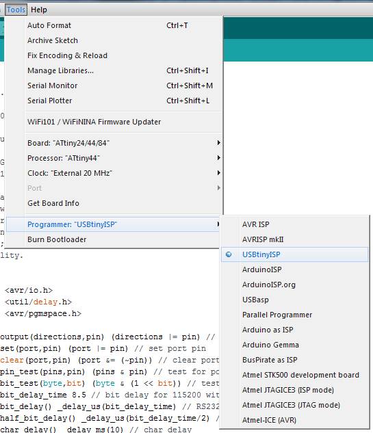
First things first, by deafult Arduino IDE does not support ATtiny. But it's reale easy thing to fix: open Preferences(File/Preferences of Ctrl+Comma)
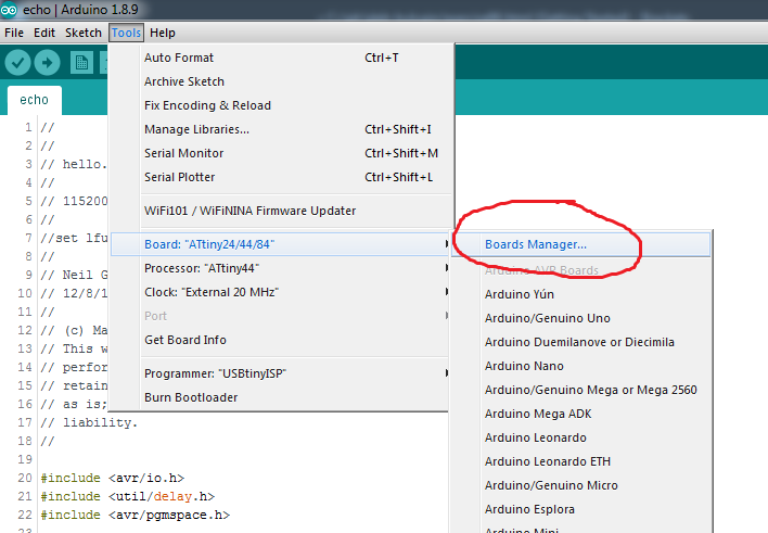

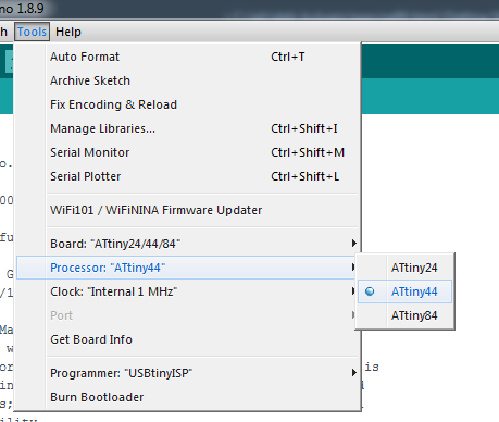
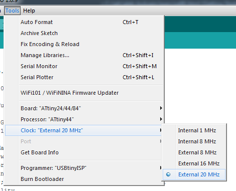
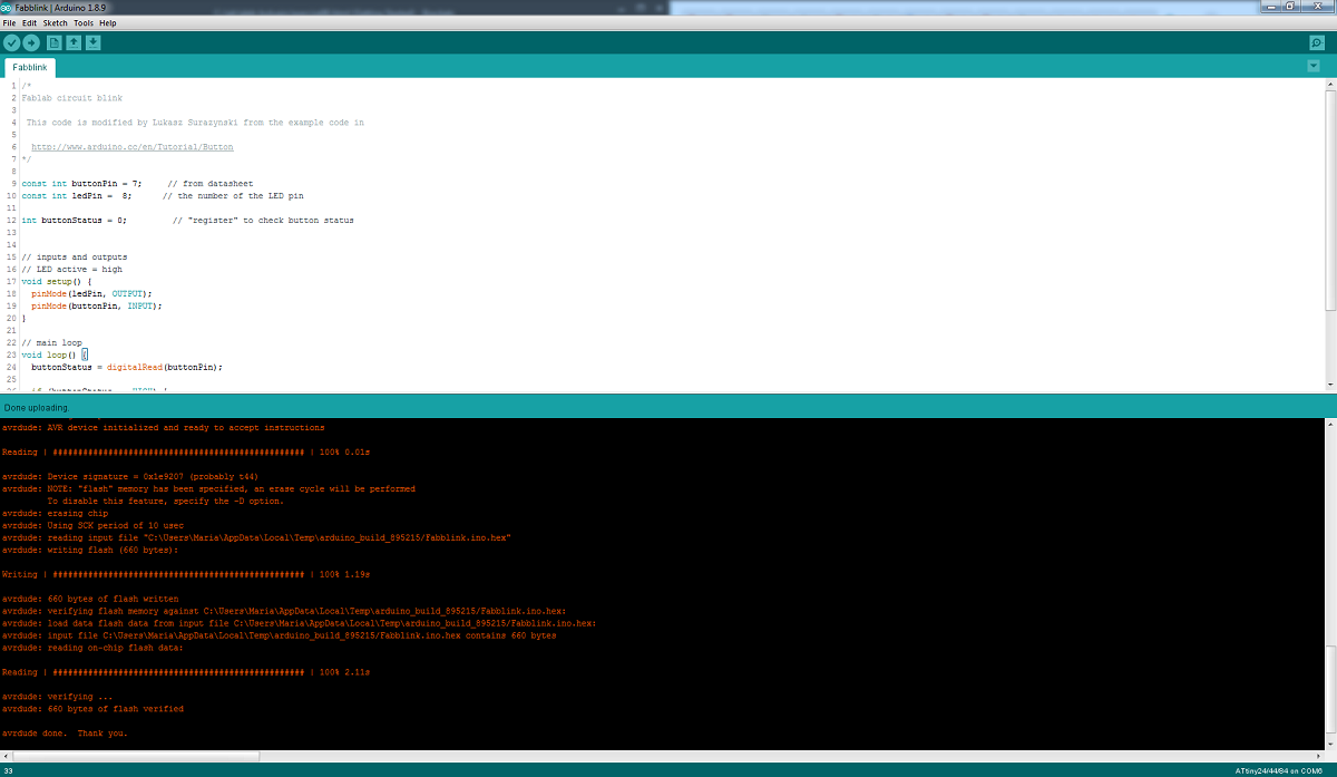
Ok, now we are ready to go. I copied the code from the hello.ftdi.44.echo.c file to an empty scketch in Arduino IDE, saved it, Verified it and Uploaded it to my board.


Then, on Antti's page I found a code sample for turning on the led by pressing button. Since he was the man who teached us the Electronics design my board looked similar and there was no need even to change the pin numbers. After I uploaded the code to my boad using my USBtinyISP programmer everything worcked from the first try.
         http://www.arduino.cc/en/Tutorial/Button

         I took this code from Antti's page:
         http://archive.fabacademy.org/archives/2016/fablaboulu/students/161/Assignment8.html

         */

        // constants won't change. They're used here to
        // set pin numbers:
        const int buttonPin = 7;     // the number of the pushbutton pin
        const int ledPin =  8;      // the number of the LED pin

        // variables will change:
        int buttonState = 0;         // variable for reading the pushbutton status

        void setup() {
            // initialize the LED pin as an output:
            pinMode(ledPin, OUTPUT);
            // initialize the pushbutton pin as an input:
            pinMode(buttonPin, INPUT);
        }

        void loop() {
            // read the state of the pushbutton value:
            buttonState = digitalRead(buttonPin);

        // check if the pushbutton is pressed.
        // if it is, the buttonState is HIGH:
        if (buttonState == HIGH) {
            // turn LED on:
            digitalWrite(ledPin, HIGH);
            }
        else {
            // turn LED off:
            digitalWrite(ledPin, LOW);
            }
        }
For the demonstration I connected the FTDI cable to a small power bank. Works as planned!
4. Results of the week
- One bricked and one fully-functional board
- I explored the main features of Eagle and got some experience which will lead me to better solutions
- So far, Arduino IDE looks like a decent choice for programming the board for my final project.
- I feel confident in circuit board milling process
- From this week I started working on a controller for my final project