Individual Assignment
Read a microcontroller data sheet, program your board to do something, with as many different programming languages and programming environments as possible
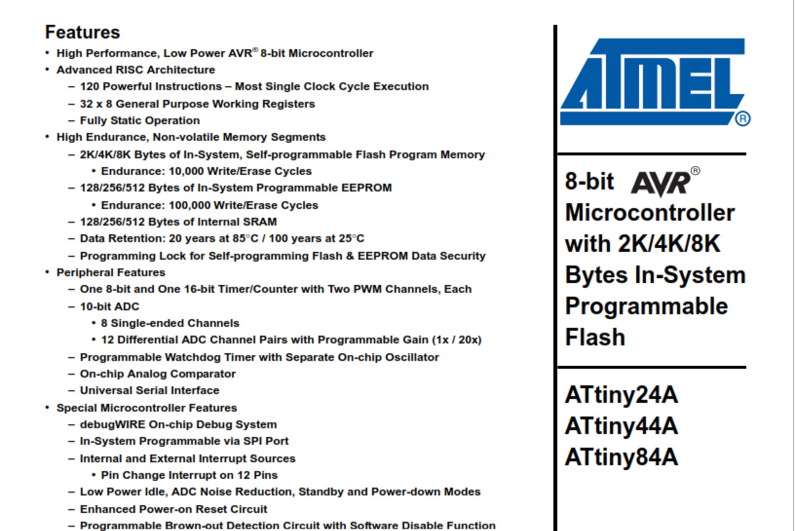
ATTiny boards Features
I had no idea, reading a datasheet was like trying to learn from a Klingon or High-Elf or what have you and now I know how a layman feels, when I lay down the IT jargon on them.
It is in no way an easy read, it takes time and lots of looking terms up, if you are unfamiliar to the abbreviations. Even if it is for a global read.
However, it is a great source for understanding how the ATTiny ICs work.
I used the datasheet to read the pin layout for week 7 and further understood the PWM feature.
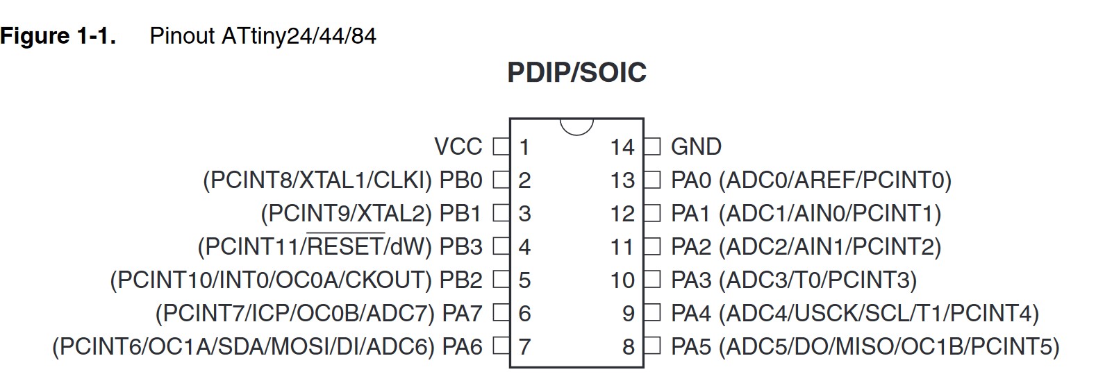
ATTiny SMD/SMT Pin Layout
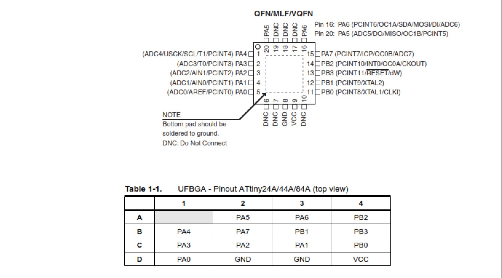
QFN....whaaaa?
*Ahem* Quad Flat No-leads Package Wiki
From my understanding in laymans terms, is that the ATTiny ICs are powerful 8Bit silicons with no to little overhead in processing instructions.
This of course is derivable from the RISC (Reduced instruction set computer) architecture, which Stanford and Berkley developed (or at least made popular) in the '80s and are perfect for embedded systems.
Further, the datasheet also explains how the pins are grouped.
The B ports are a 4-bit bi-directional I/O ports with internal pull-up resistrors. All B ports, except for PB3 (which has the RESET capability), have symmetrical driver characteristics with both high sink and source capabilities, whilst the A Ports are 8-bit bi-directional.
Port A has alternate functions as analog inputs for the ADC, analog comparator, timer/counter, SPI.
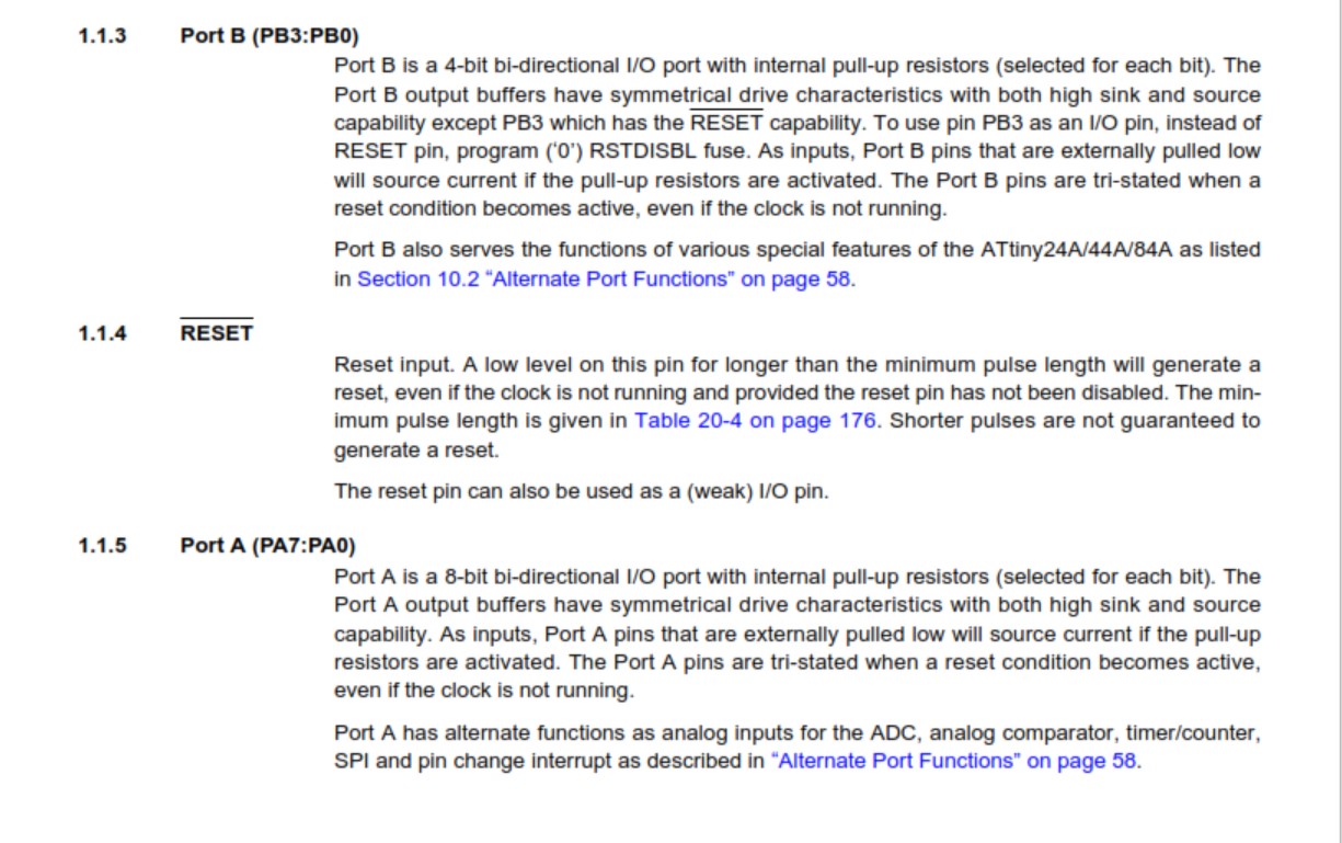
The Datasheet explains how the pins are grouped.
The pin layouts are described in groups between the PB and PA.
- The VCC and GND are the common pins and are located on pin 1 and pin 14 respectively
- Master Output Slave Input is assigned to pin 7 (PA6)
- Master In Slave Out is assigned to pin 8 (PA5)
- Serial Clock is assigned to pin 9 (PA4)
- Reset is assigned to pin 4 (PB3)
Block Diagram
ATtiny24A/44A are low-power CMOS 8-bit micro-controllers based on the AVR enhanced RISC architecture.
Attiny44A has 12 general purpose I/O lines, 32 general purpose working registers. The main function of the CPU core is to ensure correct program execution. The CPU must therefore be able to access memories, perform calculations, control peripherals, and handle interrupts.
Then the Architectural view is as shown below:
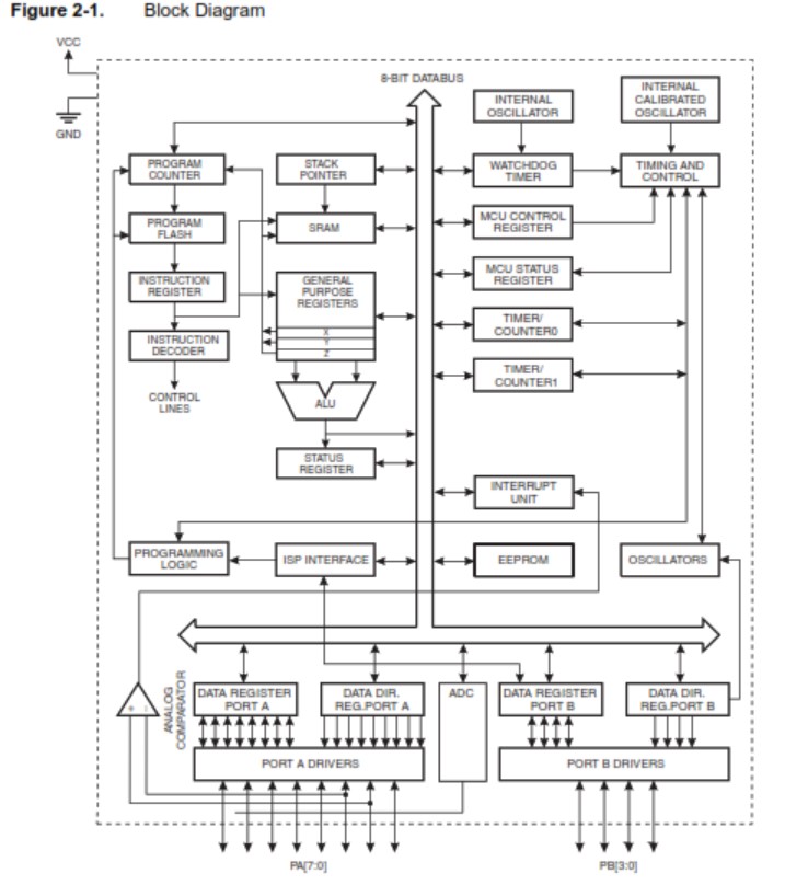
The Block Diagram
The CPU Core
The main function of the CPU core is to ensure correct program exection and must be able to access memories, preform calculations as an example.
And in order to maximize the performance and parallelism, the AVT uses a Harvard architectrue, with seperate memories and buses for program and data.
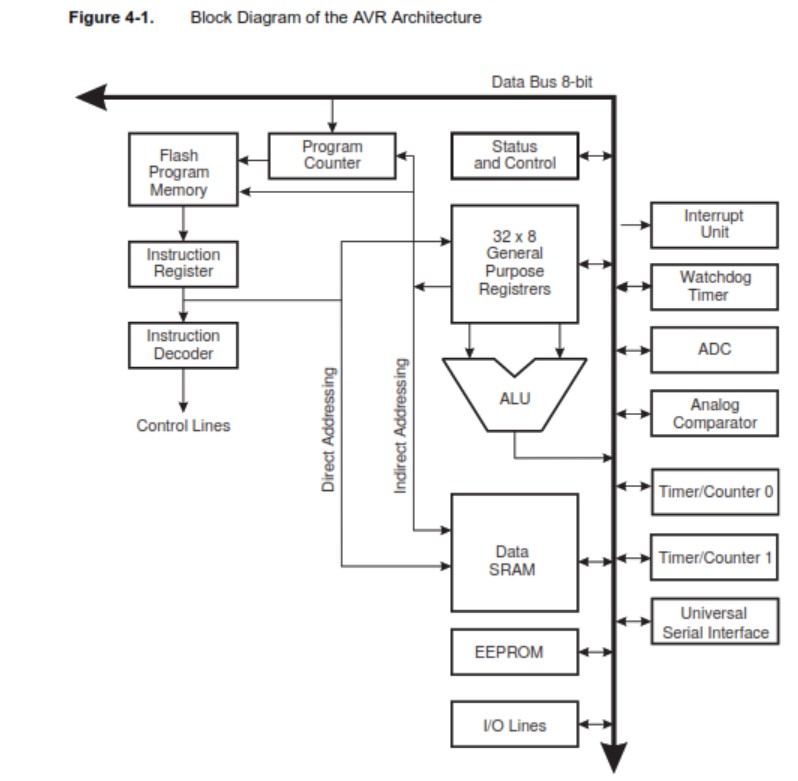
The AVR Block Diagram
Instructions in the Program memory are executed with a single level piplining as you can see in the image above.
Now I am by no means a better embedded programmer by reading the datasheet, but I have learned that the MCU of the Atmel ATTiny series is capable of being used in a pletohara of applications.
And in my case, a capacative touch sensing( I hope) midi player, with strings made of a conductive paint.
What Questions do I have, regarding the Datasheet?
Lots, to be honest, but to hone in on my main concern, how far can a single MCU go in controlling several boards?
The more refined question perhaps is, can the ATTiny series IC, control 3 boards simultaniously? i.e. A capacative strumpad, MIDI controller and MIDI board?
If it is not the ATTiny series, then maybe perhaps the ATMega series?
Guess, I will have to find out, eh?


