Week 7
Programming the Board
Program Software: Arduino IDE, Avrdude, GCC
- FabISP x 1
- Mini USB Cable x 1
- 6 Wire Ribbon Cable with Sockets x 1
- Echo Hello-World Board x 1
- FTDI Cable x 1 (秋月)
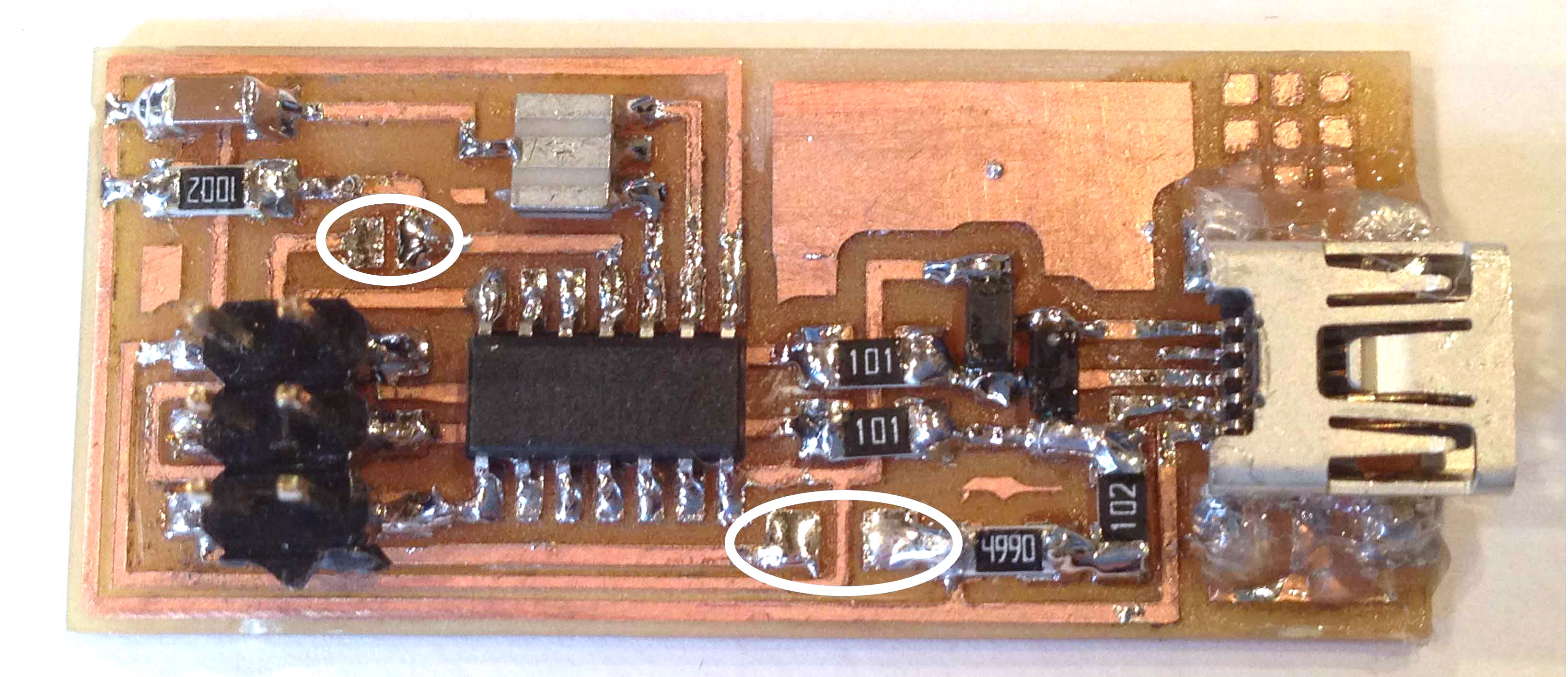
I had programmed my FabISP in week 4 but hadn’t done the last step in this tutorial, so I removed the 0 ohm resistor and solder bridge.
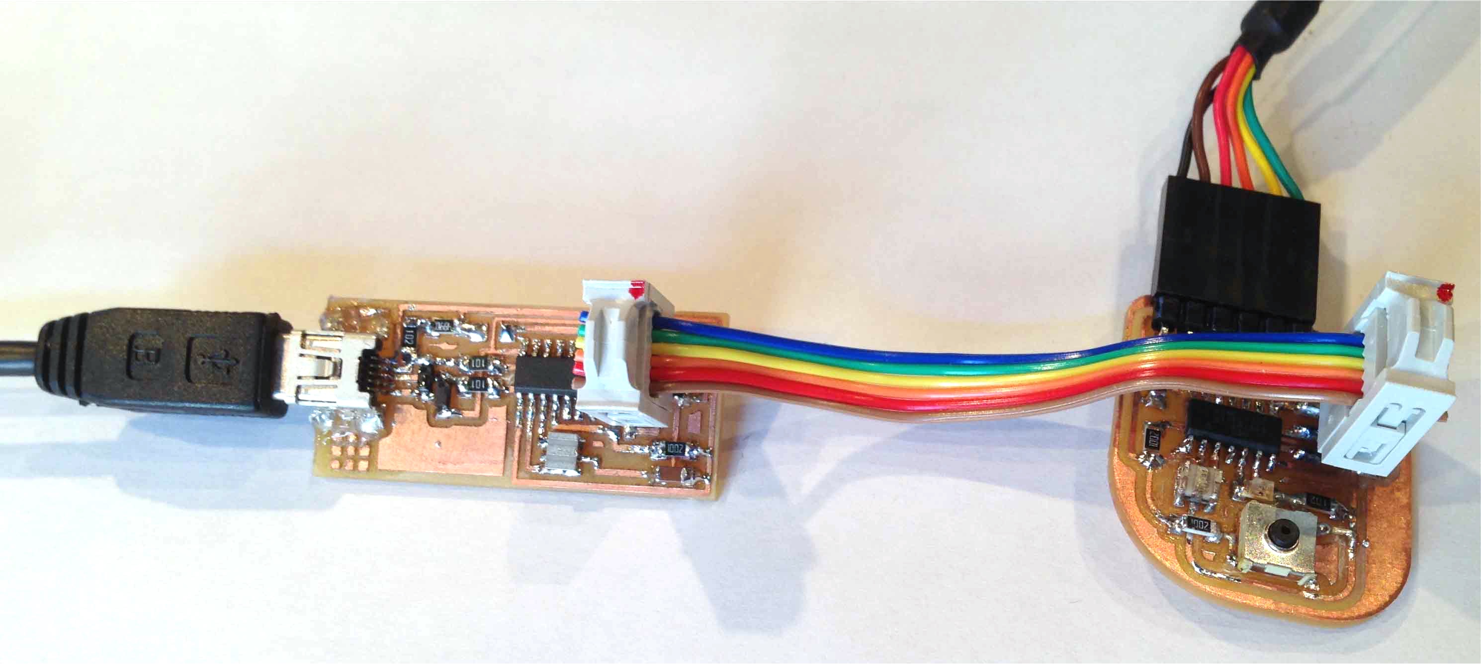
I followed this tutorial (using Arduino 1.0.6) to program my board. The Mini USB cable s connected to the FabISP to provide power and to upload the program, and the FTDI cable is connected to the led and button board to provide power. The boards’ 6-pin programming headers are connected with a 6-pin ribbon cable.
The ATtiny’s pins have corresponding Arduino Pin Numbers. For my board, the button pin is 7 and the led pin is 8.
First, I used the example code. The led tuns off while the button is pressed.
Then, I changed the example program to make the led blink whenever the button is pressed.
I also followed another tutorial to make my board echo back the computer’s keyboard input. After flashing my board and checking that the sample program worked from opening the serial monitor on Arduino IDE, I edited the code so that the board’s led will blink when it receives one character. The following is what I changed in Neil’s program.
- I added this line that states how long the led will blink
#define led_delay() _delay_ms(100) // LED blink - And these lines to set the led port
#define led_port PORTB
#define led_direction DDRB
#define led_pin (1 << PB2) - I added a function called blink().
void blink() {
set(led_port, led_pin);
led_delay();
clear(led_port, led_pin);
} - And added this line in the main loop so that the function will be called
blink();
Download
About the ATtiny44A
(Data Sheet)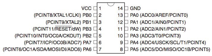
- There are 14 pins on this chip.
VCC supplies voltage.
GND is the ground.
Port B (PB3:PB0) is a 4-bit bi-directional I/O port with internal pull-up resistors.
RESET (PB3) A low level on this pin for longer than the minimum pulse length will generate a reset.
Port A (PA7:PA0) is a 8-bit bi-directional I/O port with internal pull-up resistors. Port A has alternate functions as analog inputs for the ADC, analog comparator, timer/counter, SPI and pin change interrupt. - CPU(central processing unit) ensures correct program execution by accessing memories, performing calculations, controlling peripherals, and handling interrupts.
-
There are three types of memory
Flash stores the compiled program even when the power is off (2K/4K/8K bytse).
SRAM saves temporarily variables while calculating (128/256/512 bytes).
EEPROM is for data storage (128/256/512 bytes). - ATtiny44A features successive approximation Analog-to-Digital Converter (ADC). It generates a 10-bit result which is presented in the ADC Data Registers, ADCH and ADCL. ADCL presents only the low byte of the ADC conversion result and ADCH presents only the high byte. ADCL is read first, then ADCH. When ADCH is read, ADC access to the ADCH and ADCL Registers is re-enabled and a new result is provided.